

查询SLA7024供应商
Data Sheet
SLA7024M, SLA7026M,
28201
OUT
OFF DELAY
REFERENCE
GROUND
OUT
SENSE
CNTRL SPLY
SENSE
OUT
OFF DELAY
GROUND
REFERENCE
OUT
SMA7029M
1
A
2
A
3
A
4
A
5
IN
A
6
A
7
A
8
9
B
10
B
11
B
12
B
13
B
14
IN
B
15
B
AND
SMA7029M
HIGH-CURRENT PWM, UNIPOLAR STEPPER
MOTOR CONTROLLER/DRIVERS
The SLA7024M, SLA7026M, and SMA7029M are designed for
high-efficiency and high-performance operation of 2-phase, unipolar
stepper motors. An automated, innovative packaging technology
combined with power FETs and monolithic logic/control circuitry ad-
CONTROL/LOGIC
V
REF
+
V
CC
CONTROL/LOGIC
+
V
REF
Dwg. PK-007
vances power multi-chip modules (PMCMs™) toward the complete
integration of motion control. Highly automated manufacturing techniques provide low-cost and exceptionally reliable PMCMs suitable for
controlling and directly driving a broad range of 2-phase, unipolar
stepper motors. The three stepper motor multi-chip modules differ
primarily in output current ratings (1.5 A or 3.0 A) and package style.
All three PMCMs are rated for an absolute maximum limit of 46 V
and utilize advanced NMOS FETs for the high-current, high-voltage
driver outputs. The avalanche-rated (≥100 V) FETs provide excellent
ON resistance, improved body diodes, and very-fast switching. The
multi-chip ratings and performance afford significant benefits and
advantages for stepper drives when compared to the higher dissipation
and slower switching speeds associated with bipolar transistors.
Normally, heat sinks are not required for the SLA7024M or SMA7029M.
The SLA7026M, in demanding, higher-current systems designs,
necessitates suitable heat transfer methods for reliable operation.
Complete applications information is given on the following pages.
PWM current is regulated by appropriately choosing current-sensing
resistors, a voltage reference, a voltage divider, and RC timing networks. The RC components limit the OFF interval and control current
decay. Inputs are compatible with 5 V logic and microprocessors.
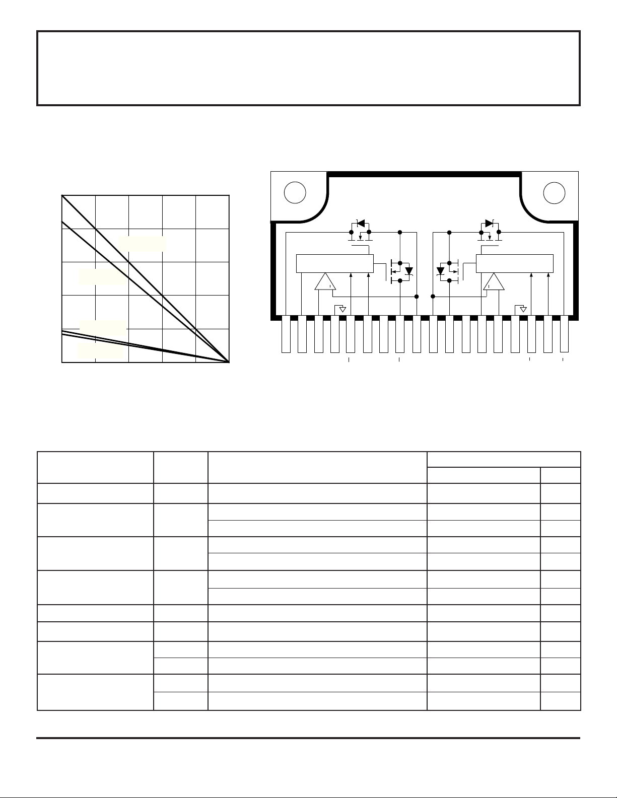
ABSOLUTE MAXIMUM RATINGS
at TA = +25°C
Load Supply Voltage, VBB. . . . . . . . . . . . 46 V
FET Output Voltage, V
Control Supply Voltage, V
Peak Output Current, I
SLA7024M . . . . . . . . . . . . . . . . . . . . . 3.0 A
SLA7026M . . . . . . . . . . . . . . . . . . . . . 5.0 A
SMA7029M . . . . . . . . . . . . . . . . . . . . 3.0 A
Continuous Output Current, I
SLA7024M . . . . . . . . . . . . . . . . . . . . . 1.5 A
SLA7026M . . . . . . . . . . . . . . . . . . . . . 3.0 A
SMA7029M . . . . . . . . . . . . . . . . . . . . 1.5 A
Input Voltage Range, V
Reference Voltage, V
Package Power Dissipation, P
Junction Temperature, T
Operating Temperature Range,
. . . . . . . . . . . . . . . . . . . . -20°C to +85°C
T
A
Storage Temperature Range,
. . . . . . . . . . . . . . . . . . -40°C to +150°C
T
stg
. . . . . . . . . . . 100 V
DS
. . . . . . . . . . 46 V
CC
(t
≤ 100 µs)
OUTM
IN
REF
w
OUT
. . . . -0.3 V to 7.0 V
. . . . . . . . . . . 2.0 V
. See Graph
D
. . . . . . . . . +150°C
J
BENEFITS AND FEATURES
■ Cost-Effective, Multi-Chip Solution
■ ‘Turn-Key’ Motion-Control Module
■ Motor Operation to 3 A and 46 V
■ 3rd Generation High-Voltage FETs
■ 100 V, Avalanche-Rated NMOS
■ Low r
NMOS Outputs
DS(on)
■ Advanced, Improved Body Diodes
■ Single-Supply Motor/Module
Operation
Always order by complete part number:
Part Number Package Output Current
SLA7024M 18-Lead Power-Tab SIP 1.5 A
SLA7026M 18-Lead Power-Tab SIP 3.0 A
SMA7029M 15-Lead SIP 1.5 A
™
■ Half- or Full-Step Unipolar Drive
■ High-Efficiency, High-Speed PWM
■ Dual PWM Current Control (2-Phase)
■ Programmable PWM Current Control
■ Low Component Count PWM Drive
■ Low Internal Power Dissipation
■ Heat Sinking (Normally) Unnecessary
■ Electrically Isolated Power Tab
■ Logic IC- and µP-Compatible Inputs
■ Machine-Insertable Package
SLA7024M, SLA7026M, AND SMA7029M
13
812915101411
853
2
467
1
14
12151011181617
13
765324198
HIGH-CURRENT PWM,
UNIPOLAR STEPPER MOTOR
CONTROLLER/DRIVERS
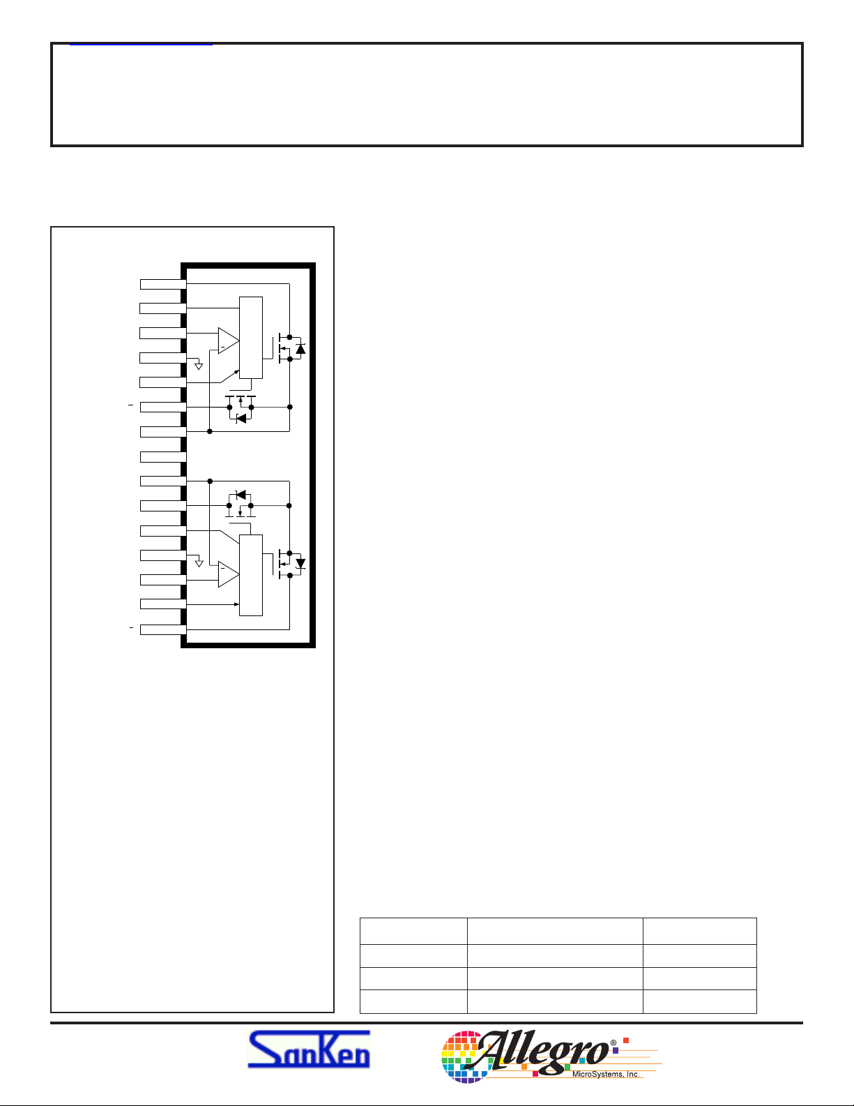
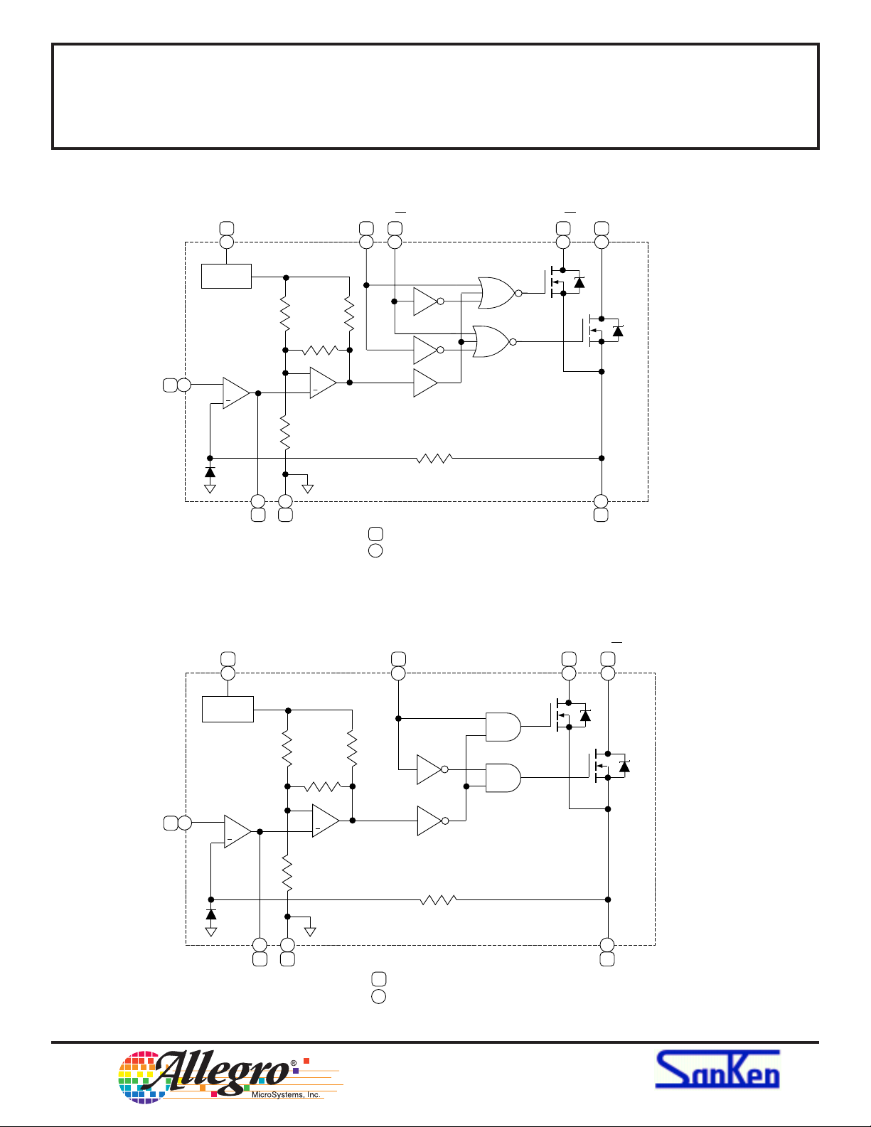
SLA7024M and SLA7026M FUNCTIONAL BLOCK DIAGRAM
CONTROL
SUPPLY
V
CC
REG.
+
REFERENCE
DELAY
Note that channels A and B are electrically isolated.
SMA7029M FUNCTIONAL BLOCK DIAGRAM
CONTROL
SUPPLY IN
IN
IN
A/B
A/B
+
CHANNEL A PIN NUMBERS
CHANNEL B PIN NUMBERS
A/B
OUT
OUT
OUT
A/B
A/B
SENSEGROUNDOFF-TIME
Dwg. FK-005
OUT
A/B
A/B
V
CC
REG.
+
REFERENCE
DELAY
+
CHANNEL A PIN NUMBERS
CHANNEL B PIN NUMBERS
SENSEGROUNDOFF-TIME
Dwg. FK-005-1
Note that except for the control supply, channels A and B are electrically isolated.
115 Northeast Cutoff, Box 15036
™
Worcester, Massachusetts 01615-0036 (508) 853-5000
Copyright © 1994 Allegro MicroSystems, Inc.
SLA7024M, SLA7026M, AND SMA7029M
HIGH-CURRENT PWM,
UNIPOLAR STEPPER MOTOR
CONTROLLER/DRIVERS
ALLOWABLE PACKAGE
POWER DISSIPATION
25
20
PREFIX 'SLA'
R = 5.0°C/W
θJM
15
PREFIX 'SMA'
R = 6.0°C/W
θJM
10
PREFIX 'SLA'
5
R = 28°C/W
θJA
PREFIX 'SMA'
R = 31°C/W
θJA
0
25
ALLOWABLE PACKAGE POWER DISSIPATION in WATTS
50 75 100 125 150
TEMPERATURE in °C
Dwg. GK-018
SLA7024M and SLA7026M
CONTROL/LOGIC
+
A
IN
CC
V
A
A
OUT
CNTRL SPLY
A
SENSE
B
SENSE
B
OUT
REF
V
12345 678910111213 14 15 16 17 18
A
A
OUT
A
OFF DELAY
A
GROUND
REFERENCE
A
IN
CONTROL/LOGIC
+
REF
CC
V
V
B
B
OFF DELAY
CNTRL SPLY
B
B
GROUND
REFERENCE
B
IN
B
IN
Dwg. PK-006
B
OUT
ELECTRICAL CHARACTERISTICS at T
= +25°C
A
Limits
Characteristic Symbol Test Conditions Min Typ Max Units
FET Leakage Current I
FET ON Voltage V
FET ON Resistance
Body Diode V
DSS
DS(ON)
r
DS(on)
SD
Forward Voltage (SLA7026M) I
Control Supply Voltage V
Control Supply Current I
Input Current I
Input Voltage V
NOTE: Negative current is defined as coming out of (sourcing) the specified device pin.
IN(H)
I
IN(L)
IN(H)
V
IN(L)
CC
CC
VDS = 100 V, VCC = 44 V — — 4.0 mA
(SLA7024M & SMA7029M) VCC = 14 V, I
(SLA7026M) V
= 14 V, I
CC
= 3 A — — 850 mV
OUT
(SLA7024M & SMA7029M) VCC = 14 V, I
(SLA7026M) V
= 14 V, I
CC
(SLA7024M & SMA7029M) I
= –3 A — 0.9 1.6 V
OUT
= 3 A — — 285 mΩ
OUT
= –1 A — 0.9 1.5 V
OUT
= 1 A — — 600 mV
OUT
= 1 A — — 600 mΩ
OUT
Operating 10 24 44 V
VCC = 44 V — 10 15 mA
VCC = 44 V, VIN = 2.4 V — — 40 µA
VIN = 0.4 V — — -800 µA
2.0 — — V
— — 0.8 V
SLA7024M, SLA7026M, AND SMA7029M
14
12151018161713
11
HIGH-CURRENT PWM,
UNIPOLAR STEPPER MOTOR
CONTROLLER/DRIVERS
TYPICAL STEPPER MOTOR APPLICATIONS
(Half of Each Device Shown)
SLA7024M and SLA7026M
V
BB
INBIN
B
V
CC
V +5 V
b
12
R 510 Ω
TO
CHANNEL
2.4 kΩ
R
5
A
REG.
V
REF
+
+
OUT
A
B
OUT
A
B
R 100 Ω
t
d
+5 V
47 kΩ
470 pF
R
C
1
3
(Device Types as Designated)
WAVE DRIVE (FULL STEP)
for SLA7024M and SLA7026M
Sequence 0 1 2 3 0
Input A H L L L H
Input A L L H L L
Input B L H L L L
Input B L L L H L
Output ON A B A B A
HALF-STEP OPERATION (2-1-2 SEQUENCE)
for SLA7024M, SLA7026M, and SMA7029M
Sequence 0 1 2 345670
Input A H H L LLLLHH
Input A or tdA*LLLHHHLLL
Input B L H H H LLLLL
Input B or tdB*LLLLLHHHL
Output(s) ON A AB B A B A AB B A B A
*Logic signals to external open-collector inverter connected to tdA and tdB.
C 2200 pF
3
TRUTH TABLES
2-PHASE (FULL STEP) OPERATION
for SLA7024M and SLA7026M
Sequence 0 1 2 3 0
Input A H L L H H
Input A L H H L L
Input B H H L L H
Input B L L H H L
Outputs ON AB A B AB A B AB
SENSE
R
S
≤1 Ω
Dwg. EK-008
115 Northeast Cutoff, Box 15036
™
Worcester, Massachusetts 01615-0036 (508) 853-5000

13
8
12
9
10
14
11
15
SLA7024M, SLA7026M, AND SMA7029M
HIGH-CURRENT PWM,
UNIPOLAR STEPPER MOTOR
CONTROLLER/DRIVERS
TYPICAL STEPPER MOTOR APPLICATIONS
(Half of Device Shown)
SMA7029M
V
BB
IN
B
V
CC
V +5 V
b
12
R 510 Ω
TO
CHANNEL
A
2.4 kΩ
R
5
REG.
V
REF
+
+
OUT
A
B
OUT
A
B
R 100 Ω
t
d
C
+5 V
OPEN-COLLECTOR
INVERTER
R 47 kΩ
3
1
470 pF C 2200 pF
TRUTH TABLES
(SMA7029M Only)
WAVE DRIVE (FULL STEP) for SMA7029M
Sequence 0 1 2 3 0
Input A H L L L H
Input tdA* L L H L L
Input B L H L L L
Input tdB* L L L H L
Output ON A B A B A
*Logic signals to external open-collector inverter connected to tdA and tdB.
SENSE
3
R
S
≤1 Ω
2- PHASE (FULL STEP) OPERATION
for SMA7029M
Sequence 0 1 2 3 0
Input A H H L L H
Input B L H H L L
Outputs ON A B AB A B AB A B
Dwg. EK-008-1

SLA7024M, SLA7026M, AND SMA7029M
HIGH-CURRENT PWM,
UNIPOLAR STEPPER MOTOR
CONTROLLER/DRIVERS
APPLICATIONS INFORMATION
REGULATING THE PWM OUTPUT CURRENT
The output current (and motor coil current) waveform is illustrated in
Figure 1. Setting the PWM current trip point requires various external
components:
Vb = Reference supply (typically 5 V)
R1, R2 = Voltage-divider resistors in the reference supply circuit
RS = Current sensing resistor(s)
NOTE: The maximum allowable V
input voltage is 2.0 V.
REF
The voltage-divider must be selected accordingly.
Normal PWM (Full-Current/Running) Mode
I
is set to meet the specified running current for the motor (Figure 2)
OUT
and is determined by:
V
≈
≈
PHASE A
PHASE A
REF
R
S
R
2
R1 + R
0
V
b
•
R
2
S
or, if V
I
OUT
is not known
REF
I
OUT
FIGURE 1. PHASE A COIL CURRENT WAVEFORM
V
b
V
INPUT
CC
V
I
BB
OUT
(1)
(2)
Dwg. WK-001
R
PEAK
CURRENT
DETECTOR
3
C
1
t
d
PWM
OFF-TIME
CONTROL
CONTROL
LOGIC
R
1
R
R
5
2
V
REF
C
3
FIGURE 2. PWM CONTROL (RUN MODE)
115 Northeast Cutoff, Box 15036
Worcester, Massachusetts 01615-0036 (508) 853-5000
AA
CURRENT
CONTROL
&
RECIRCULATING
CURRENT
CONTROL
SENSE
R
S
B
B
Dwg. EK-009
™

SLA7024M, SLA7026M, AND SMA7029M
HIGH-CURRENT PWM,
UNIPOLAR STEPPER MOTOR
CONTROLLER/DRIVERS
For given values of R1, R2, and Vb (V
≈ 0.82 V), Figure 3 illustrates
REF
output current as a function of current-sensing resistance (RS).
3.0
2.5
2.0
1.5
1.0
0.5
OUTPUT TRIP CURRENT in AMPERES
SLA7026M MAX.
R1 = 510 Ω
R
2
= 100 Ω
X
= ∞
R
V
b
= 5 V
SLA7024M & SMA7029M MAX.
0
0 1.5 2.5 3.5
0.5 1.0 2.0 3.0 4.0
CURRENT-SENSING RESISTANCE in OHMS
Dwg. GK-014
FIGURE 3. CURRENT-SENSING RESISTANCE
Reduced/Holding Current Mode
Additional circuitry (Figure 4) enables reducing motor current. The
external transistor changes the voltage-divider ratio, V
output current. I
is determined by resistors R2 and RX in parallel:
HOLD
, and reduces the
REF
I
HOLD
or
I
HOLD
where R
R2 R
≈
X
R1 R2 + R1 RX + R2 R
R
’
2
≈
R1 + R
2
’
= the equivalent value of R2 and RX in parallel.
2
HOLD
•
’ R
V
b
S
R
X
V
b
•
R
X
S
V
b
R
1
R
5
R
C
2
V
REF
3
FIGURE 4. HOLD CURRENT MODE
SENSE
R
S
(3)
(4)
Dwg. EK-010

SLA7024M, SLA7026M, AND SMA7029M
HIGH-CURRENT PWM,
UNIPOLAR STEPPER MOTOR
CONTROLLER/DRIVERS
For given values of R1, R2, and Vb (V
≈ 0.82 V), Figures 5A and 5B
REF
illustrate output holding current as a function of RX for two values of currentsensing resistance (RS).
1.0
RS = 0.8 Ω
0.8
0.6
0.4
0.2
OUTPUT TRIP CURRENT in AMPERES
0
0 300 500
100 200 400 600
HOLDING-CURRENT RESISTANCE in OHMS
R1 = 510 Ω
R2 = 100 Ω
Vb = 5 V
RS = 1.0 Ω
Dwg. GK-015
FIGURE 5A. HOLD-CURRENT RESISTANCE
(SLA7024M and SMA7029M)
3.0
R1 = 510 Ω
2.5
2.0
1.5
1.0
OUTPUT TRIP CURRENT in AMPERES
0.5
0
0 300 500 700
R
2
= 100 Ω
V
b
= 5 V
100 200 400 600 800
HOLDING-CURRENT RESISTANCE in OHMS
RS = 0.33 Ω
RS = 0.47 Ω
Dwg. GK-015-1
FIGURE 5B. HOLD-CURRENT RESISTANCE (SLA7026M)
NOTE: Holding current determines holding torque, which is normally
greater than running torque. Consult motor manufacturer for recommended
safe holding current and motor winding temperature limits in “standstill” or
“detent” mode.
The MOSFET outputs create ringing noise with PWM, but the RC filter
precludes malfunctions. The comparator operation is affected by R5 and C
and, thus, current overshoot is influenced by component values. Empirical
adjustment to “fine-tune” the current limit is likely.
3
115 Northeast Cutoff, Box 15036
Worcester, Massachusetts 01615-0036 (508) 853-5000
™

SLA7024M, SLA7026M, AND SMA7029M
HIGH-CURRENT PWM,
UNIPOLAR STEPPER MOTOR
CONTROLLER/DRIVERS
DETERMINING THE MOTOR PWM FREQUENCY
The modules function asynchronously, with PWM OFF time fixed by R
and C1 at input td. The OFF time can be calculated as:
t
≈ -R3 • C1 • logn (1 - 2 ) (5)
OFF
Recommended circuit constants and t
Vb = 5 V
R3 = 47 kΩ
C1 = 470 pF
t
= 12 µs
OFF
50
3
V
b
are:
OFF
40
RS = 1 Ω
L/R = 1 to 3 ms
30
20
ON TIME in µs
10
0
0 6 10 14
24 8 12
MOTOR RESISTANCE in OHMS
VCC = 24 V
VCC = 36 V
20
25
30
35
40
CHOPPING FREQUENCY in kHz
Dwg. GK-016
FIGURE 7.
PWM FREQUENCY vs MOTOR RESISTANCE
POWER DISSIPATION CALCULATIONS
Excepting high-current applications utilizing the SLA7026M above
approximately 2.0 A at +65°C (with 2-phase operation), the need for heat
sinks is rare. The basic constituents of conduction losses (internal power
dissipation) include:
(a) FET output power dissipation (I
(b) FET body diode power dissipation (VSD • I
OUT
2
• r
DS(on)
OUT
or I
), and
OUT
• V
DS(ON)
),
(c) control circuit power dissipation (VCC • ICC).
Device conduction losses are calculated based on the operating mode
(wave drive, half-step, or 2-phase). Assuming a 50% output duty cycle:
Wave Drive = 0.5 (I
Half-Step = 0.75 (I
2-Phase = (I
OUT
2
• r
OUT
2
• r
OUT
2
• r
DS(on)
) + (VSD • I
) + 0.5 (VSD • I
DS(on)
) + 0.75 (VSD • I
DS(on)
OUT
) + (V
OUT
OUT
• 15 mA)
CC
) + (V
) + (V
• 15 mA)
CC
• 15 mA)
CC

SLA7024M, SLA7026M, AND SMA7029M
HIGH-CURRENT PWM,
UNIPOLAR STEPPER MOTOR
CONTROLLER/DRIVERS
PACKAGE RATINGS/DERATING FACTORS
Thermal ratings/deratings for the multi-chip module packages vary
slightly. Normally, the SLA7024M and SMA7029M do not need heat
sinking when operated within maximum specified output current (≤1.0 A
with 2-phase drive) unless the design ambient temperature also exceeds +60°C. Thermal calculations must also consider the temperature
effects on the output FET ON resistance. The applicable thermal
ratings for the PMCM packages are:
SLA7024M and SLA7026M 18-Lead Power-Tab SIP
R
= 28°C/W (no heat sink) or 4.5 W at +25°C and a derating
ΘJA
factor of -36 mW/°C for operation above +25°C. R
SMA7029M 15-Lead SIP
R
= 31°C/W (no heat sink) or 4.0 W at +25°C and a derating
ΘJA
factor of -32 mW/°C for operation above +25°C. R
= 5°C/W.
ΘJC
= 6°C/W.
ΘJC
TEMPERATURE EFFECTS ON FET r
DS(on)
Analyzing safe, reliable operation includes a concern for the
relationship of NMOS ON resistance to junction temperature. Device
package power calculations must include the increase in ON resistance
(producing higher output ON voltages) caused by higher operating
junction temperatures. Figure 8 provides a normalized ON resistance
curve, and all thermal calculations should consider increases from the
given +25°C limits, which may be caused by internal heating during
normal operation.
2.5
2.0
1.5
1.0
0.5
NORMALIZED FET ON RESISTANCE
0
-40 +80 +160
0
+40 +120
JUNCTION TEMPERATURE in °C
FIGURE 8. NORMALIZED ON RESISTANCE
vs TEMPERATURE
115 Northeast Cutoff, Box 15036
Worcester, Massachusetts 01615-0036 (508) 853-5000
Dwg. GK-017
™

SLA7024M, SLA7026M, AND SMA7029M
HIGH-CURRENT PWM,
UNIPOLAR STEPPER MOTOR
CONTROLLER/DRIVERS
SLA7024M and SLA7026M
Dimensions in Inches
(for reference only)
1.22
±0.008
0.126
±0.006
ø
0.630
±0.008
118
0.026
0.961
0.646
±0.008
1.232
+0.008
–0.004
±0.008
±0.008
0.126
0.390
0.022
0.066
±0.016
±0.006
0.189
±0.008
±0.008
0.512
±0.008
0.264
±0.020
+0.008
–0.004
x 0.150
0.067
±0.004
0.096
±0.008
0.118
0.157
±0.028
3.2
±0.15
Dwg. MK-002-18 in
Dimensions in Millimeters
(controlling dimensions)
3.2
±0.15
0.55
±0.2
13
x 3.8
6.7
±0.5
+0.2
–0.1
4.0
±0.7
4.8
±0.2
1.7
±0.1
2.45
±0.2
3.0
Dwg. MK-002-18 mm
31
±0.2
24.4
16.4
±0.2
±0.2
±0.2
ø
±0.2
16
9.9
118
31.3
±0.2
+0.2
0.65
–0.1
1.68
±0.4
NOTES: 1. Exact body and lead configuration at vendor’s option within limits shown.
2. Recommended mounting hardware torque: 4.34 – 5.79 lbf•ft (6 – 8 kgf•cm or 0.588 – 0.784 Nm).
3. The hatched area is exposed (electrically isolated) heat spreader.
4. Recommend use of metal-oxide-filled, alkyl-degenerated oil base, silicone grease (Dow Corning 340 or equivalent).

SLA7024M, SLA7026M, AND SMA7029M
HIGH-CURRENT PWM,
UNIPOLAR STEPPER MOTOR
CONTROLLER/DRIVERS
SMA7029M
Dimensions in Inches
(for reference only)
1.24
MAX.
1.22
±0.008
0.402
±0.008
115
+0.008
0.026
–0.004
0.335
0.080
±0.004
MAX.
0.022
30°
0.157
±0.008
0.264
±0.020
+0.008
–0.004
0.157
±0.028
0.098
±0.008
0.057
±0.006
0.118
Dimensions in Millimeters
(controlling dimensions)
31.5 MAX.
31±0.2
±0.2
10.2
115
+0.2
0.65
–0.1
NOTE: Exact body and lead configuration at vendor’s option within limits shown.
The products described here are manufactured in Japan by Sanken Electric Co.,
Ltd. for sale by Allegro MicroSystems, Inc.
Sanken Electric Co., Ltd. and Allegro MicroSystems, Inc. reserve the right to
make, from time to time, such departures from the detail specifications as may be
required to permit improvements in the design of their products.
The information included herein is believed to be accurate and reliable.
However, Sanken Electric Co., Ltd. and Allegro MicroSystems, Inc. assume no
responsibility for its use; nor for any infringements of patents or other rights of third
parties which may result from its use.
2.03
±0.1
8.5
MAX.
0.55
30°
4.0
±0.2
6.7
±0.5
+0.2
–0.1
4.0
±0.7
Dwg. MK-005-15 mm
Dwg. MK-005-15 in
2.5
±0.2
1.45
±0.15
3.0
115 Northeast Cutoff, Box 15036
Worcester, Massachusetts 01615-0036 (508) 853-5000
™
 Loading...