


SEPW Series
Multi Chip White LED Modules
Features and Benefits
▪ High efficiency, 100 1m/W (20 mA ) with all LEDs
illuminated; equivalent to fluorescent lamps (HCFL)
▪ Low thermal resistance, R
= 6°C/W
θJC
▪ High optical, 50 lm, output with all LEDs illuminated
▪ Superior directivity
▪ 5.23 mm × 13.7 mm case footprint, and
low 2.5 mm overall package height
▪ Silver plating on leadframe
▪ 8 LED configuration
Package:
16-pin, 1.27 mm pitch, surface mount
Description
The SEPW series of LEDs provides a range of high-powered
InGaN blue LEDs producing brilliant white light that can be
used in general lighting applications, amusement and gaming
equipment, and for backlighting TFT displays. Each module
combines 8 LEDs in 2 separate channels.
Modular design allows the SEPW devices to be easily assembled
into string arrays by simply connecting the modules in series.
The devices also provide superior color balance throughout
the display because of the high density of LEDs that can be
achieved. This also minimizes the distance that power and
control lines must run between LEDs and from the LEDs to
the control electronics.
The white thermoplastic case is an innovative Sanken original
design with exceptional heat dissipation properties. The white
resin compound is especially formulated for superior reflectance
and transmittance of the generated light. Enhanced thermal
dissipation is achieved through the incorporated heatsink on the
bottom of the package. The heatsink can be mated directly to an
external radiator through the PCB for superior heat conduction
allowing dense placement of modules.
The leadframe is plated with silver, providing a highly-reflective
surface for the bottom and sides of the emitting area. The
terminals and heatsink are also silver-plated.
Not to scale
V
B
5 to 20 V
5 V
Use only
one dimming
method
C
COMP
48100.000, Rev. 4
R
0.1 μF
10 V
FSET
L1
10 μH
1 μF
35 V
R
ISET
SW SW OVP
SEL1
SEL2
SEL3
VIN
LED Driver
EN
PWM
APWM
SKIP
COMP
FSET
ISET
AGND
PGND LGND
D1
Allegro
A8500
IC
R
OVP
C
O
2.2 μF/50 V
LED1
LED2
LED3
LED4
LED5
LED6
LED7
LED8
T ypical Application
8 SEPW modules, 8 LEDs each
SEP8W
SEP8W
SEP8W
SEP8W
SEP8W
SEP8W
SEP8W
SEP8W
R
C
R
R
The SEPW devices can be mounted in tight
arrays on a single PCB substrate for ease of
manufacture and to provide a dense, uniform
appearance when illuminated.
The application shown here uses eight
SEP8Wx2001 LED modules, each populated
by eight LEDs connected in series.
OVP
COMP
ISET
FSET
100 kΩ
0.1 μF / 6.3 V
12.7 kΩ (for 20.3 mA)
26.1 kΩ (for 1 MHz
switching frequency)
SEPW Series
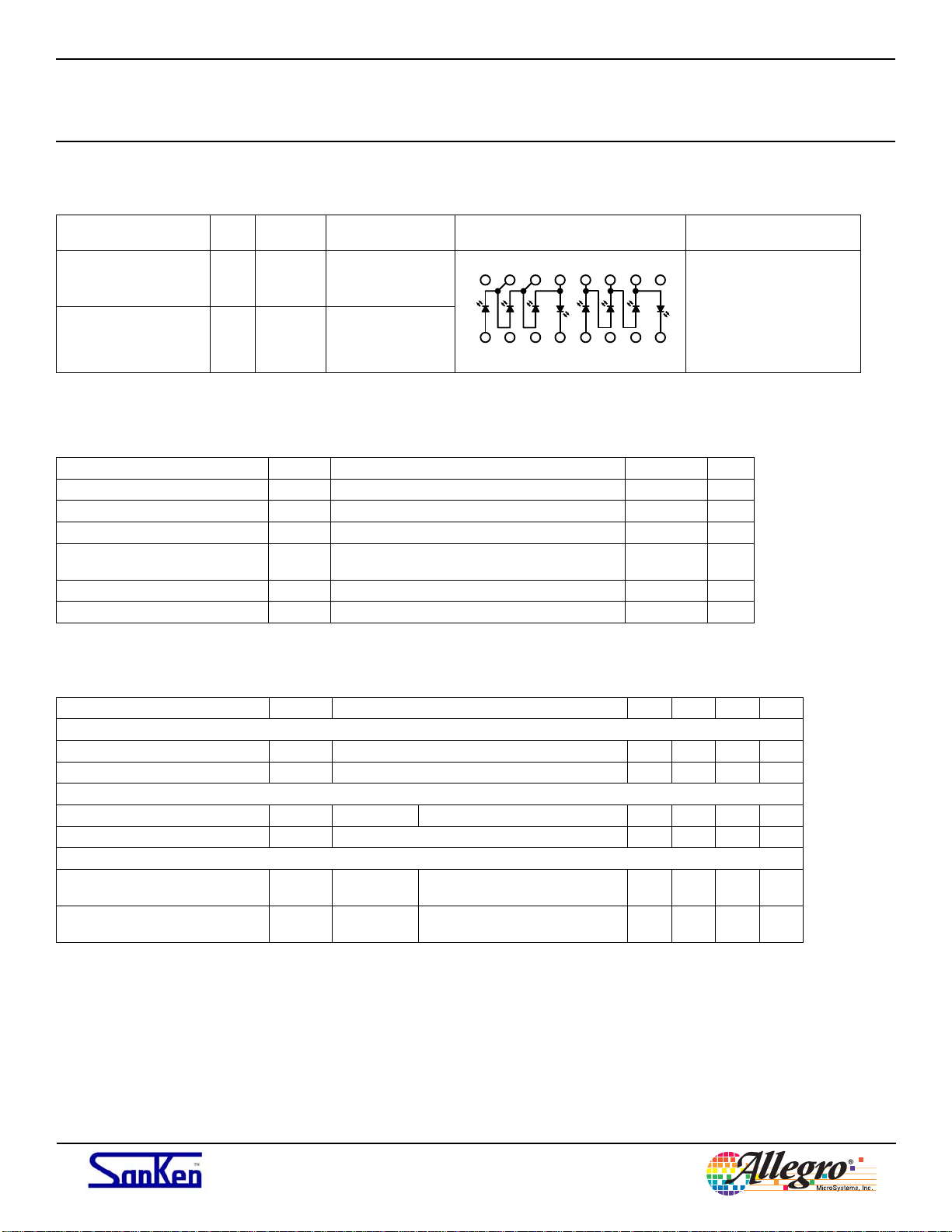
Selection Guide
Part Number LEDs Channels Color Temperature
Multi Chip White LED Modules
Internal Circuit Diagram
(Pin Numbers Shown)
Packing
SEP8WL2001 8 2 Bulb Light (2900)
16 15 14 13 12 11 10 9
B BBB BB
SEP8WN2001 8 2 Day White (5000)
12345678
Absolute Maximum Ratings (electrical characteristics at TA=25°C)
Characteristic Symbol Notes Rating Units
Forward Current (Continuous) I
Forward Current (Pulsed) I
Reverse Voltage V
Isolation Voltage V
Operating Temperature T
Storage Temperature T
Per element 40 mA
f
Frequency, f = 1 kHz, pulse width, tw = 100 μs 100 mA
fp
R
Measured from device pins to heatsink, with DC
IS
voltage applied
opr
stg
Operating Characteristics
Characteristic Symbol Conditions Min. Typ. Max. Units
Electrical
Forward Voltage (per LED channel) V
Reverse Current (per LED channel) I
Optical
Luminous Flux (all channels) Φ SEP8Wx 8 LEDs, I
Peak Wavelength λ
Thermal
Thermal Resistance (junction to
exposed thermal pad)
Thermal Resistance (junction to
ambient)
R
R
If = 20 mA, TA = 25˚C 2.6 3.1 3.8 V
f
VR = 5 V – – 10 μA
R
= 20 mA / LED 25 40 – lm
f
If = 20 mA TA = 25°C – 460 – nm
P
SEP8Wx 8 LEDs – 6 – °C/W
θJC
All SEPxWx – 120 – °C/W
θJA
BB
5V
±60 V
–40 to 85 °C
–40 to 90 °C
1000 pieces per reel
All performance characteristics given are typical values for circuit or
system baseline design only and are at the nominal operating voltage and
an ambient temperature, T
, of 25°C, unless oth er wise stated.
A
Allegro MicroSystems, Inc.
115 Northeast Cutoff, Box 15036
Worcester, Massachusetts 01615-0036 (508) 853-5000
www.allegromicro.com
2

SEPW Series
Chromaticity and Color Temperature (JIS Z9112-2004) at TA = 25°C, If= 20 mA
Day White WN Yes
Bulb Light WL Yes
Color Symbol JIS Compliant
Multi Chip White LED Modules
x
(±0.01)
0.3616 0.3875
0.3552 0.3476
0.3324 0.3296
0.3326 0.3635
0.4834 0.4382
0.4594 0.3971
0.4153 0.3862
0.4305 0.4218
y
(±0.01)
Color Temperature (Center)
(K)
4600 to 5500
(5000)
2600 to 3250
(2900)
Chromaticity Diagram (Compliance with CIE1931)
0.50
0.45
0.40
Y
0.35
0.30
0.25
0.20
0.20 0.25 0.30 0.35 0.40 0.45 0.50
:1
Planckian Locus
X
:/
Allegro MicroSystems, Inc.
115 Northeast Cutoff, Box 15036
Worcester, Massachusetts 01615-0036 (508) 853-5000
www.allegromicro.com
3

SEPW Series
Short Axis
Long Axis
Module
Top View
–50
Multi Chip White LED Modules
SEPW Series Directivity
TA= 25°C, If = 20 mA
0
–10
–20
–30 30
–40
10
20
Degrees from Normal
40
Common in Long and Short Axes
50
–80
–90
–70
–60
60
70
80
90
050100
Relative Emission Intensity
Emission Color Mixing
Additive white light
Silicone resin
with mixed
fluorescent material
Blue LED
Emission Spectrum (Typical)
TA= 25°C, If = 20 mA
Day White (WN) Bulb Light (WL)
1.2
1.0
0.8
0.6
0.4
0.2
Relative Emission Intensity Factor
0
380 480 580 680 780
Emission Wavelength (nm) Emission Wavelength (nm)
Allegro MicroSystems, Inc.
115 Northeast Cutoff, Box 15036
Worcester, Massachusetts 01615-0036 (508) 853-5000
www.allegromicro.com
1.2
1.0
0.8
0.6
0.4
0.2
Relative Emission Intensity Factor
0
380 480 580 680 780
4

SEPW Series
Multi Chip White LED Modules
Forward Current versus Foward Voltage
T
= 25°C
A
100
(mA)
f
I
10
2.70 2.90 3.10 3.30 3.50 3.70 3.90
(V)
V
f
Forward Voltage versus Ambient Temperature
= 20 mA
I
f
3.10
3.00
2.90
(V)
f
V
2.80
slope = –17 mV/°C
Relative Luminous Flux versus
Forward Current, T
3.50
3.00
2.50
2.00
1.50
1.00
Relative & Factor
0.50
0
020406080100
= 25°C
A
If (mA)
Relative Luminous Flux versus
Ambient Temperature, I
1.00
80
60
40
Relative & (%)
20
= 20 mA
f
2.70
0 20 40 60 80 100 120
TA (°C)
Forward Current versus Duty Cycle
T
= 25°C, tw≤ 100 μs
A
120
100
80
60
(mA)
f
40
I
20
0
110100
Duty Cycle (% On)
Allegro MicroSystems, Inc.
115 Northeast Cutoff, Box 15036
Worcester, Massachusetts 01615-0036 (508) 853-5000
www.allegromicro.com
0
020406080100120
TA (°C)
Allowable Forward Voltage versus Ambient
Temperature at Various Thermal Resistances
50
40
30
(V)
f
V
20
R
θ
JA
R
θJA
= 30°C/W
=50°C/W
R
θJA
= 15°C/W
Without Heatsink
R
θJA
10
0
= 120°C/W
020406080100
TA (°C)
5

SEPW Series
Multi Chip White LED Modules
Chromaticity versus Forward Current (Typical)
TA= 25°C
0.39
SEPxWN Target
Chromaticity Range
0.38
0.37
0.36
y
0.35
0.34
0.33
0.32
0.32 0.33 0.34 0.35 0.36 0.37 0.38
30 mA
10 mA
60 mA
40 mA
50 mA
20 mA
x
Chromaticity versus Ambient Temperature
If = 20 mA
0.45
0.44
0.43
0.42
y
0.41
0.4
0.39
0.38
SEPxWL Target
Chromaticity Range
60 mA
40 mA
20 mA
0.41 0.42 0.43 0.44 0.45 0.46 0.47 0.48 0.49
10 mA
50 mA
30 mA
x
y
0.39
0.38
0.37
0.36
0.35
0.34
0.33
0.32
SEPxWN Target
Chromaticity Range
50
60
°C
°C
40
70
°C
°C
25
0.45
0.44
0.43
0.42
°C
0.35 0.36 0.37 0.380.32 0.33 0.34
x
Allegro MicroSystems, Inc.
115 Northeast Cutoff, Box 15036
Worcester, Massachusetts 01615-0036 (508) 853-5000
www.allegromicro.com
y
0.41
0.40
0.39
0.38
SEPxWL Target
Chromaticity Range
60°C
70°C
50°C
40°C
25°C
0.45 0.48 0.490.41 0.42 0.43 0.44 0.470.46
x
6

SEPW Series
Multi Chip White LED Modules
Package Outline Drawing
Device is lead (Pb) free.
Allegro MicroSystems, Inc.
115 Northeast Cutoff, Box 15036
Worcester, Massachusetts 01615-0036 (508) 853-5000
www.allegromicro.com
7

SEPW Series
Multi Chip White LED Modules
Solder Pad Layout
Allegro MicroSystems, Inc.
115 Northeast Cutoff, Box 15036
Worcester, Massachusetts 01615-0036 (508) 853-5000
www.allegromicro.com
8

SEPW Series
Multi Chip White LED Modules
Embossed Tape and Reel Specifi cation
Taping reel dimensions (1/4)
Embossed taping outline dimensions (1/1)
330±2
8
.
0
±
0
.
1
2
φ
φ13.0±0.2
Label
29.4±1.0
25.4±1.0
100±1
Pull direction
No LEDsLEDs mounting partNo LEDs
Top cover tape
Reel Lead Min. 160 mm
Detailed drawing (1/1)
Anode mark
Tolerance ±0.2
P4.0
Embossed carrie r tape
φ1.5
2.0
φ1.5P12.0
1000 pcs/reel
0.34
1.75
11.5
14.5
3.7
9.2
Allegro MicroSystems, Inc.
115 Northeast Cutoff, Box 15036
Worcester, Massachusetts 01615-0036 (508) 853-5000
www.allegromicro.com
Accmulative tol erance per 10 pitches shall be ±0.2 mm.
Adhesion streng th shall be 0.1-0.7 N when the cov er tape and
the carrier ta pe are torn o at the angle of 10 deg rees.
24.0
P/N, manufacturing date code number and quantitiy shall be indicated on
moist-proof package.
Reel Lead (No LEDs) Min. 320 mm
Reel Lead Min. 400 mm
9

SEPW Series
WARNING — These devices are designed to be operated at lethal voltages and energy levels. Circuit designs
that embody these components must conform with applicable safety requirements. Pre cau tions must be
taken to prevent accidental contact with power-line potentials. Do not connect ground ed test equipment.
The use of an isolation transformer is recommended during circuit development and breadboarding.
This product series emits high light output. Do NOT look directly into the light emitting area. Direct
exposure to the light over an extended time period may harm eyes.
Multi Chip White LED Modules
Because reliability can be affected adversely by improper storage
environments and handling methods, please observe the following:
Cautions for Storage
• Ensure that storage conditions are within 5°C to 40°C and relative
humidity < 30%; avoid storage locations that experience extreme
changes in temperature or humidity.
• Avoid locations where dust or harmful gases are present and
avoid direct sunlight.
• Reinspect for rust on leads and solderability of products that have
been stored for a long time.
Cautions for Testing and Handling
When tests are carried out during inspection testing and other
standard test periods, protect the products from power surges
from the testing device, shorts between adjacent products, and
shorts to the heatsink.
Precautions During Use
• Because the light generated inside the LED must be emitted
efficiently out of the module, a resin with high light transmittance
is used. Therefore, additives that are commonly used in
semiconductor devices to improve the heat resistance or moisture
resistance (such as silica glass) cannot be added to the resin.
Consequently, the ability of the resin to withstand heat is usually
low and the following precautions must be observed.
• Never apply an external force, stress, or excess vibration to resin
or terminals when at high temperature.
• Take particular care about heat dissipation when designing the
application. If dissipation is not adequate, the LEDs can reach
high temperatures, with resulting color change, luminous flux
reduction, and shortening of product lifetime.
• When the device is connected to an external radiator, please
coat the heatsink area with thermal conduction material such as
thermal conductive bond or thermal conductive grease.
• Extra attention should be paid to the sealing resin of the product,
which is rubber-like silicon resin. The surface of sealing resin is
slightly sticky (surface tack). Therefore, touching the emitting area
or exposing it to unclean conditions may cause dust or smudges
to adhere to it and possibly penetrate the resin. This could
cause deterioration of product characteristics when contacted by
materials such as epoxy resin.
• The silver plating of the leadframe may discolor if the product
comes into contact with material containing sulfides or if it is
exposed to an atmosphere containing sulfide gas.
• The emitting area of the LEDs contains fine gold wires. Touching
this area without care may add excess stress on the internal gold
wires and may result in disconnection of the internal wires.
Soldering
• The product is in a surface mount package. The product should
not be mounted on warped direction of the PCB.
• When the product is mounted by means of solder reflow and the
resin is unusually damp, solder dipping may cause interfacial
defoliation. This occurs when a drastic temperature change
causes moisture in the resin to evaporate and to swell. Therefore,
attention must be paid to the following:
• Examine the moisture-resistant packing before opening. If
the indicator color (blue) of the desiccant (such as silica gel)
has disappeared, the product must be prebaked as described
below.
• After the product packing is opened and staged for assembly,
soldering should be carried out as soon as practicable.
• During handling, ambient conditions should be 5°C to 30°C,
with relative humidity < 70%
• After 120 hours of exposure, prebake is recommended
before soldering; bake-out at 60±5°C for more than 10 hours
• After soldering, no mechanical force or excessive vibration should
be applied to the product until the product has cooled down to
normal room temperature. Quick cooling must be avoided.
• When soldering the products, please be sure to minimize the
working time, within the following limits:
Soldering Iron Temperature
(°C)
Time
(s)
350±10 3 (once only)
• Reflow soldering can be performed a maximum of 2 times, with
preheat conditions of 150°C to 180°C (at the device surface)
for 60 to 120 s, and soldering conditions less than 40 s at more
than 220°C, with a peak temperature less than 260°C, using the
following recommended profile:
Reflow Soldering Profile
300
260
220
180
140
100
60
20
Temperature of Device Package Surface (°C)
0 50 100 150 200 250 300
Peak 260°C Max
Pre-heat
60 to 120 sec
Soldering Time (s)
40 sec
Max
Between the first and second reflow sessions, follow the
guidelines in the Cautions for Storage section, above.
Electrostatic Discharge
• When handling the products, operator must be grounded.
Grounded wrist straps worn should have at least 1 MΩ of
Allegro MicroSystems, Inc.
115 Northeast Cutoff, Box 15036
Worcester, Massachusetts 01615-0036 (508) 853-5000
www.allegromicro.com
10

SEPW Series
Multi Chip White LED Modules
resistance to ground to prevent shock hazard.
• Workbenches where the products are handled should be
grounded and be provided with conductive table and floor mats.
• When using measuring equipment such as a curve tracer, the
equipment should be grounded.
• When soldering the products, the head of soldering irons or the
solder bath must be grounded in other to prevent leak voltages
generated by them from being applied to the products.
• The products should always be stored and transported in our
shipping containers or conductive containers, or be wrapped in
Power Supply
Bypass
Capacitor
0.1 μF
R
10 kΩ
Protective Circuit
Reference Circuit Using Capacitor Reference Circuit Using Zener Diode
C
>0.01 μF
Resistor
aluminum foil.
• Exposure to any overvoltage exceeding the Absolute Maximum
Rating of the products may cause damage to, or possibly result in
destruction of, the products. Buyer shall take absolutely secured
countermeasures against static electricity and surge when
handling the products.
• Typical anti-static and anti-surge reference circuits are shown
below. The circuits shown are for reference only, and the buyer
must make a sufficient experimental verification of the static and
surge levels when employing the product.
Resistor
1X per LED
ZD
VR 7 to 8 V
Protective Circuit
Application and operation examples described in this document are quoted for the sole purpose of reference only, for the use of the products
herein, and Sanken can assume no responsibility for any infringement of industrial property rights, intellectual property rights, or any other rights
of Sanken or any third party which may result from its use.
When using the products herein, the applicability and suitability of such products for an intended purpose or object shall be reviewed at the
user’s responsibility.
Although Sanken undertakes to enhance the quality and reliability of its products, the occurrence of failure and defect of semiconductor products at a certain rate is inevitable. Users of Sanken products are requested to take, at their own risk, preventative measures including safety design
of the equipment or systems against any possible injury, death, fires or damages to the society due to device failure or malfunction.
Sanken products listed in this document are designed and intended for the use as components in general purpose electronic equipment or apparatus (home appliances, office equipment, telecommunication equipment measuring equipment, etc.). Before placing an order, the user’s written
consent to the specifications is requested.
When considering the use of Sanken products in the applications where higher reliability is required (transportation equipment and its control
systems, traffic signal control systems or equipment, fire/crime alarm systems, various safety devices, etc.), please contact your nearest Sanken
sales representative to discuss and obtain written confirmation of your specifications.
The use of Sanken products without the written consent of Sanken in the applications where extremely high reliability is required (aerospace
equipment, nuclear power control systems, life support systems, etc.) is strictly prohibited.
Anti radioactive ray design is not considered for the products listed herein.
If there is any discrepancy between English and Japanese versions of this datasheet, the Japanese version should take precedence over the
English one.
Please accept in advance that the content of this datasheet is subject to change without notice for the purpose of such as improvement of the
product.
Copyright © 2007-2008 Allegro MicroSystems, Inc. This datasheet is based on Sanken datasheet 92019.
Allegro MicroSystems, Inc.
115 Northeast Cutoff, Box 15036
Worcester, Massachusetts 01615-0036 (508) 853-5000
www.allegromicro.com
11

SEPW Series
Asia-Pacific
Multi Chip White LED Modules
Worldwide Contacts
China
Sanken Electric Hong Kong Co., Ltd.
Suite 1026, Ocean Centre, Canton Road
Tsimshatsui, Kowloon, Hong Kong
Tel: 852-2735-5262, Fax: 852-2735-5494
Sanken Electric (Shanghai) Co., Ltd.
Room 3202, Maxdo Centre, Xingyi Road 8
Changning District, Shanghai, China
Tel: 86-21-5208-1177, Fax: 86-21-5208-1757
Taiwan Sanken Electric Co., Ltd.
Room 1801, 18th Floor, 88 Jung Shiau East Road
Sec. 2, Taipei 100, Taiwan R.O.C.
Tel: 886-2-2356-8161, Fax: 886-2-2356-8261
India
Saket Devices Pvt. Ltd.
Office No. 13, First Floor, Bandal-Dhankude Plaza
Near PMT Depot, Paud Road
Kothrud, Pune 411 038, India
Tel: 91-20-5621-2340, 91-20-2528-5449
Fax: 91-20-2528-5459
Japan
Sanken Electric Co., Ltd.
Overseas Sales Headquarters
Metropolitan Plaza Building, 1-11-1 Nishi-Ikebukuro
Toshima-ku, Tokyo 171-0021, Japan
Tel: 81-3-3986-6164, Fax: 81-3-3986-8637
Korea
Sanken Electric Korea Co., Ltd.
Mirae Asset Life Building, 6F
168 Kongduk-dong, Mapo-ku
Seoul 121-705, Korea
Tel: 82-2-714-3700, Fax: 82-2-3272-2145
Singapore
Sanken Electric Singapore Pte. Ltd.
150 Beach Road, #14-03 The Gateway West
Singapore 189720
Tel: 65-6291-4755, Fax: 65-6297-1744
Europe
Sanken Power Systems (UK) Limited
Pencoed Technology Park
Pencoed, Bridgend CF35 5HY, United Kingdom
Tel: 44-1656-869-100, Fax: 44-1656-869-162
North America
United States
Allegro MicroSystems, Inc.
115 Northeast Cutoff
Worcester, Massachusetts 01606, U.S.A.
Tel: 1-508-853-5000, Fax: 1-508-853-7895
Allegro MicroSystems, Inc.
14 Hughes Street, Suite B105
Irvine, California 92618, U.S.A.
Tel: 1-949-460-2003, Fax: 1-949-460-7837
Allegro MicroSystems, Inc.
115 Northeast Cutoff, Box 15036
Worcester, Massachusetts 01615-0036 (508) 853-5000
www.allegromicro.com
12
 Loading...