

Page 1
STR-S6411 and STR-S6411F
123456789
OFF-LINE SWITCHING REGULATORS
STR-S6411 AND
STR-S6411F
OFF-LINE SWITCHING REGULATORS
– WITH POWER MOSFET OUTPUT
These devices are specifically designed to meet the requirements
for increased integration and reliability in off-line flyback (STR-S6411)
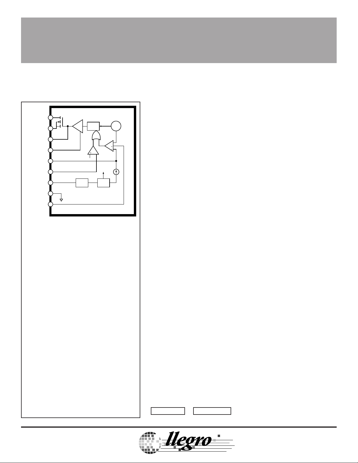
DRAIN
SOURCE
GATE
POWER
GROUND
SOFT
START
OVER-CURRENT
PROTECTION
V
SIGNAL
GROUND
FDBK
REF.
PWM
OSC.
+
Dwg. PK-003
LATCH
+
IN
UVLO
and forward (STR-S6411F) converters operating in a fixed-frequency
PWM mode. Each device incorporates the primary control and drive
circuits with an avalanche-rated high-voltage power MOSFET. Crucial
system parameters such as switching frequency and maximum duty
cycle are fixed during manufacture. The STR-S6411 and STR-S6411F
differ only in their maximum duty cycle. Control circuit decoupling and
layout are optimized within each device.
Cycle-by-cycle and average-current limiting, soft start, undervoltage lockout with hysteresis, and thermal shutdown protect the
device during all normal and overload conditions. The performance and
reliability of these devices, and their variable-frequency counterparts,
has been proven in substantial volume production.
The requirements of high dielectric isolation and low transient
thermal impedance and steady-state thermal resistance are satisfied in
an over-molded, 9-pin single in-line power package.
Data Sheet
28101.1
ABSOLUTE MAXIMUM RATINGS
Supply Voltage, VIN............................ 35 V
Drain-Source Voltage, VDS............... 800 V
Drain Current, I
continuous ..................................... ±5 A
single pulse, tw ≤1 ms .................. ±20 A
Avalanche Energy, E
single pulse............................... 400 mJ
Gate-Source Voltage, VGS................ ±20 V
Gate-Drive Current Range,
IG................................. -0.7 A to +1.5 A
Over-Current Protection Voltage Range,
V
............................. -0.3 V to +4.0 V
OCP
Insulation RMS Voltage,
V
WM(RMS)
DISCONTINUED PRODUCT
Package Power Dissipation,
PD........................................ See Graph
FET Channel Temperature, TJ...... +150°C
Internal Frame Temperature, TF... +125°C
Operating Temperature Range,
TA............................... -20°C to +125°C
Storage Temperature Range,
T
............................. -30°C to +125°C
stg
D
A
..................................... 2000 V
— FOR REFERENCE ONLY
FEATURES
■ PWM Flyback Conversion or Forward Conversion
■ Output Power to 250 W
■ Pulse-by-Pulse Current Limiting
■ Fixed-Frequency 100 kHz PWM
■ Avalanche-Rated Power MOSFET Switch
■ Soft Start
■ Internal Under-Voltage Lockout and Thermal Shutdown
■ Low External Component Count
■ Over-Molded SIP with Isolated Heat Spreader
Always order by complete part number:
STR-S6411 or STR-S6411F .
TM
TM
A
MicroSystems, Inc.
Page 2
STR-S6411 and STR-S6411F
OFF-LINE SWITCHING REGULATORS
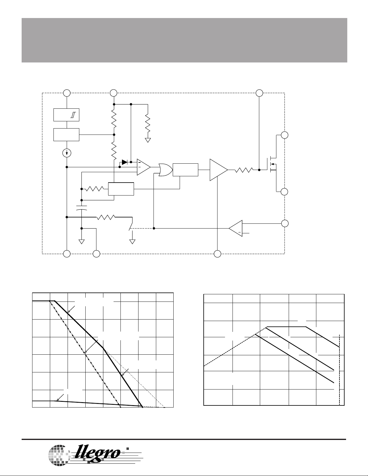
FUNCTIONAL BLOCK DIAGRAM
V
UVLO
IN
7
FDBK
9
GATE
3
REF.
5
SOFT
START
R
toff
8
SIGNAL
GROUND
R
ton
PWM
+
OSC.
R
LATCH
S
Q
4
POWER
GROUND
+
0.2 V
DRAIN
1
SOURCE
2
OVER-CURRENT
6
PROTECTION
Dwg. FK-003
ALLOWABLE PACKAGE POWER DISSIPATION MAXIMUM SAFE OPERATING AREA
62 W
60
MOUNTING SURFACE
TEMPERATURE
100
RECOMMENDED MAX.
40
20
FREE AIR
3.2 W
ALLOWABLE PACKAGE POWER DISSIPATION in WATTS
0
20 60 100
A
FRAME TEMP. = +100°C
TEMPERATURE in °C
MicroSystems, Inc.
LIMITED BY FRAME
TEMP. = +125°C MAX.
TM
TM
30
LIMITED
BY r
DS(on)
NO HEAT SINK
NATURAL COOLING
T = +25°C
A
10 30 100 300
DRAIN-TO-SOURCE VOLTAGE in VOLTS
140
Dwg. GK-003
10
3.0
1.0
DRAIN CURRENT in AMPERES
0.3
0.1
3.0
115 Northeast Cutoff, Box 15036
W
Worcester, Massachusetts 01615-0036 (508) 853-5000
Copyright © 1994 Allegro MicroSystems, Inc.
t = 0.1 ms SINGLE PULSE
w
t = 1 ms SINGLE PULSE
w
t = 10 ms SINGLE PULSE
w
DS
LIMITED BY V max
1000
Dwg. GK-004-1
Page 3
STR-S6411 and STR-S6411F
OFF-LINE SWITCHING REGULATORS
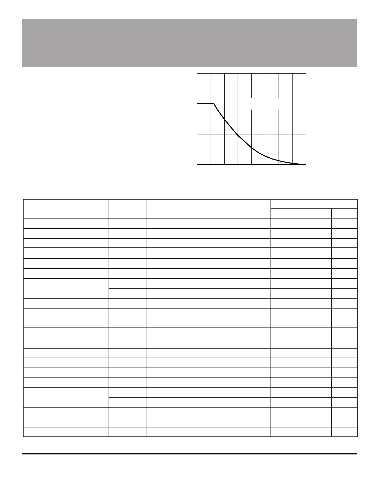
600
500
400
ALLOWABLE AVALANCHE ENERGY
300
200
100
ALLOWABLE AVALANCHE ENERGY in mJ
0
0 60 100
SINGLE PULSE
DRAIN CURRENT = 5 A
SUPPLY VOLTAGE = 50 V
20 40 80 120 160
STARTING CHANNEL TEMPERATURE in °C
140
Dwg. GK-009-1
ELECTRICAL CHARACTERISTICS at T
= +25°C, VIN = 17 V, voltage measurements are referenced to
A
Signal Ground (pin 8) (unless otherwise noted).
Limits
Characteristic Symbol Test Conditions Min. Typ. Max. Units
On-State Voltage V
Under-Voltage Lockout V
FET Leakage Current I
FET ON Resistance r
DS(on)
Forward Transconductance g
FET Input Capacitance C
Propagation Delay Time t
Oscillator Frequency f
Maximum ON Time t
INT
INQ
DSS
fs
iss
phl
t
plh
osc
on
Turn-on, increasing V
Turn-off, decreasing V
IN
IN
14.4 16 17.6 V
8.4 9.4 10.4 V
VDS = 800 V – – 1.2 mA
VGS = 10 V, ID = 3 A – 1.8 2.2 Ω
VGS = 10 V, ID = 3 A 3.0 – – S
VDS=10 V, VGS=0 V, f=1 MHz – 1800 – pF
Turn-on, 10% VGS to 10% V
Turn-off, 90% VGS to 90% V
DS
DS
–60– ns
– 140 – ns
93 100 107 kHz
STR-S6411 5.1 5.7 6.5 µs
STR-S6411F 3.8 4.5 5.2 µs
Over-Current Threshold V
OCP Current I
Feedback Current I
Soft Start Threshold Voltage V
Soft Start Current I
Power Ground Current I
Supply Current I
I
IN(OFF)
Insulation RMS Voltage V
WM(RMS)
OCP(th)
OCP
FDBK
SS(th)
SS
PG
IN(ON)
VSS = 0 V – -100 – µA
tw = 200 ns – -1.0 -1.5 A
Operating – 23 – mA
Start up, VIN = 12 V – – 500 µA
All terminals simultaneous reference 2000 – – V
160 200 240 mV
-250 -400 -550 µA
– -1.8 – mA
– – 0.4 V
metal plate against backside
Thermal Resistance R
θJM
FET channel to mounting surface – 2.0 – °C/W
NOTES: Negative current is defined as coming out of (sourcing) the specified device terminal.
Typical Data is for design information only.
Page 4

STR-S6411 and STR-S6411F
OVER-CURRENT THRESHOLD VOLTAGE in mV
OFF-LINE SWITCHING REGULATORS
TYPICAL CHARACTERISTICS
160
140
120
100
80
OSCILLATOR FREQUENCY in kHz
60
40
-20 40 80
0 20 60 100 140
AMBIENT TEMPERATURE in °C
300
120
Dwg. GK-005
35
30
25
20
15
10
OPERATING SUPPLY CURRENT in mA
5
0
0
V
INQ
510 203040
INPUT VOLTAGE in VOLTS
T = +100°C
A
V
INT
15 25
T = +25°C
A
T = -20°C
A
35
Dwg. GK-006
A
250
200
150
100
50
0
TM
TM
MicroSystems, Inc.
0 20 60 100 140
-20 40 80
AMBIENT TEMPERATURE in °C
115 Northeast Cutoff, Box 15036
Worcester, Massachusetts 01615-0036 (508) 853-5000
120
Dwg. GK-007
Page 5

STR-S6411 and STR-S6411F
OFF-LINE SWITCHING REGULATORS
TYPICAL PWM FLYBACK CONVERSION USING STR-S6411
WARNING: lethal potentials are present. See text.
NC
39
AC INPUT
220 V/240 V
RECTIFIER
FULL-BRIDGE
7
+
STR-S6411
+ OUTPUT
+
1
+
2
VOLTAGE
SENSE
– OUTPUT
AC INPUT
220 V/240 V
RECTIFIER
FULL-BRIDGE
+
8
5
4
6
Dwg. EK-003-2
TYPICAL PWM FORWARD CONVERSION USING STR-S6411F
WARNING: lethal potentials are present. See text.
+ OUTPUT
NC
7
+
STR-S6411F
39
+
1
+
2
VOLTAGE
SENSE
– OUTPUT
+
5
8
4
6
Dwg. EK-003-3
Page 6

STR-S6411 and STR-S6411F
OFF-LINE SWITCHING REGULATORS
APPLICATIONS INFORMATION
WARNING — These devices are designed to be operated at lethal voltages and energy levels.
Circuit designs that embody these components must conform with applicable safety requirements.
Precautions must be taken to prevent accidental contact with power-line potentials.
Do not connect grounded test equipment.
The use of an isolation transformer is recommended during circuit development and breadboarding.
The power MOSFET outputs of these devices are similar to the International Rectifier type IRFPE40. These devices
feature an excellent combination of fast switching, ruggedized device design, low on-resistance, and cost effectiveness.
Recommended mounting hardware torque:
4.34 - 5.79 lbf•ft (6 – 8 kg•cm or 0.588 – 0.784 Nm).
Recommended metal-oxide-filled, alkyl-degenerated oil base, silicone grease:
Dow Corning 340, or equivalent
±0.012
1.49
0.033
+0.008
–0.004
0.118
1
0.016
Dimensions in Inches
(Based on 1 mm = 0.03937")
0.953
±0.008
T REF.
0.610
±0.008
9
M
0.130
±0.008
±0.008
0.709
0.100
±0.004
ø
0.177
±0.028
0.216
±0.008
0.130
±0.004
0.276
±0.016
0.216
0.026
+0.008
–0.004
A
PACKAGE
CENTER
TM
TM
MicroSystems, Inc.
LEAD
CENTER
NOTE: Exact body and lead configuration at vendor’s option within limits shown.
115 Northeast Cutoff, Box 15036
Worcester, Massachusetts 01615-0036 (508) 853-5000
Dwg. MK-003-9 in
Page 7

STR-S6411 and STR-S6411F
OFF-LINE SWITCHING REGULATORS
Dimensions in Millimeters
24.2
±0.2
T REF
15.5
3.0
±0.2
3.3
±0.2
M
ø
5.5
±0.2
±0.3
23.0
0.85
+0.2
–0.1
1
0.4
PACKAGE
CENTER
±0.2
18.0
3.3
±0.1
7.0
±0.4
5.5
9
2.54
±0.1
0.65
+0.2
–0.1
4.5
±0.7
LEAD
CENTER
NOTE: Exact body and lead configuration at vendor’s option within limits shown.
Dwg. MK-003-9 mm
Page 8

STR-S6411 and STR-S6411F
OFF-LINE SWITCHING REGULATORS
POWER CONVERSION/POWER MANAGEMENT
SELECTION GUIDES
SWITCHING REGULATOR PMCMs
Part
Number* Application AC In Max P
5703 Quasi-Resonant Flyback Converter 110/120 V 140 W 500 V 6 A Bipolar
5707 Quasi-Resonant Flyback Convertter 85-265 V 90 W 850 V 6 A Bipolar
220/240V 140 W
5708 Quasi-Resonant Flyback Converter 85-265 V 120 W 850 V 7.5 A Bipolar
220/240 V 180 W
6511 Quasi-Resonant Flyback Converter 110/120 V 180 W 450 V 11 A MOSFET
6703 Quasi-Resonant Flyback Converter 110/120V 140 W 500 V 6 A Bipolar
6704 Quasi-Resonant Flyback Converter 110/120 V 100 W 500 V 5 A Bipolar
O
Power Switch
6707 Quasi-Resonant Flyback converter 85-265 V 90 W 850 V 6 A Bipolar
220/240 V 140 W
6708 Quasi-Resonant Flyback Converter 85-265 V 120 W 850 V 7.5 A Bipolar
220/240 V 180 W
6709 Quasi-Resonant Flyback Converter 85-265 V 160 W 850 W 10 A Bipolar
220/240 V 220 W
* Complete part number includes additional characters to indicate operating temperature range and package style.
LINEAR REGULATOR ICs
Part
Number* V
8184 3.0 V 10 V 300 mV @ 125 mA 250 mA SOT-89
8187 3.3 V 10 V 300 mV @ 125 mA 250 mA SOT-89
8188 2.5–3.3 V 10 V 300 mV @ 125 mA 250 mA SOT-89
8188 2.5–3.3 V 10 V 300 mV @ 125 mA 250 mA SOIC
* Complete part number includes additional characters to indicate operating temperature range and package style.
Also — 83145 and 84145 Latched, Universal Input-Voltage Switches.
O
Max DC In Max Dropout Max I
O
Package
Allegro MicroSystems, Inc. reserves the right to make, from time to time, such
departures from the detail specifications as may be required to permit improvements
in the design of its products. Components made under military approvals will be in
accordance with the approval requirements.
The information included herein is believed to be accurate and reliable.
However, Allegro MicroSystems, Inc. assumes no responsibility for its use; nor for
any infringements of patents or other rights of third parties which may result from its
use.
TM
A
TM
MicroSystems, Inc.
115 Northeast Cutoff, Box 15036
Worcester, Massachusetts 01615-0036 (508) 853-5000
 Loading...