

查询ATS673供应商
Self-Calibrating TPOS Gear Tooth Sensor Optimized for
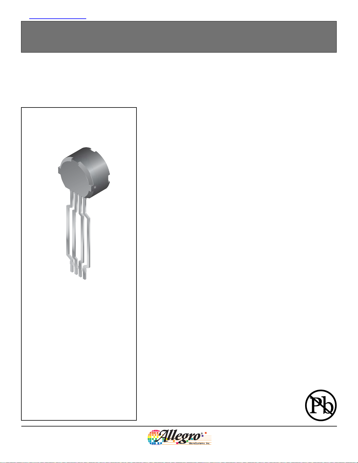
Package SE, 4-pin Through Hole
ATS673 and ATS674
Automotive Cam Sensing Applications
Recognizing the increasingly stringent requirements for EMC/EMI in automotive
applications, Allegro has taken the necessary steps to design devices that are
capable of withstanding the effects of radiated and conducted transients. The
ATS673 and ATS674 devices have been designed specifically for this purpose.
Advanced circuitry on the die allows them to survive positive and negative
transient pulses on both the input and output.
The ATS673 and ATS674 devices retain all of the same characteristics as the
ATS671 and ATS672. The devices remain true zero-speed gear tooth sensors with
optimized Hall IC/magnet configuration in an SIP (single in-line package). The
SIP assembly consists of a molded package that holds together a samarium cobalt
magnet, a pole piece, and a true zero-speed Hall IC that has been optimized to the
magnetic circuit.
1
2
3
1. VCC
2. VOUT
3. TEST
4. GND
4
AB SO LUTE MAX I MUM RAT INGS
Supply Voltage, VCC...........................................28 V
Reverse-Supply Voltage, V
Continuous Output Current, I
Reverse-Output Current, I
Operating Temperature
Ambient, T
Maximum Junction, T
Storage Temperature, T
, Range L................–40ºC to 150ºC
A
........................–18 V
RCC
...................20 mA
OUT
.......................50 mA
ROUT
........................165ºC
J(max)
.................. –65ºC to 170ºC
S
The sensor incorporates a single element Hall IC that switches in response to
magnetic signals created by a ferrous target. The IC contains a sophisticated
digital circuit designed to eliminate the detrimental effects of magnet and system
offsets. Signal processing is used to provide zero-speed performance independent
of air gap and also to dynamically adapt device performance to the typical
operating conditions found in automotive applications, particularly cam sensing
applications (reduced vibration sensitivity).
High-resolution (9-bit) peak detecting DACs are used to set the adaptive switching
thresholds of the devices, ensuring high accuracy even in the presence of gear
eccentricity. Hysteresis in the thresholds reduces the negative effects of anomalies
in the magnetic signal (such as magnetic overshoot) associated with the targets
used in many automotive applications. The ATS673 and 674 also include a low
bandwidth filter that increases the noise immunity and the signal to noise ratio of
the sensor.
Two options are available for output polarity, low over tooth (LT) and high over
tooth (HT). For applications requiring absolute accuracy use the ATS674. The
ATS673 should be used for targets with high wobble.
Features and Benefits
Tight timing accuracy over operating temperature range
True zero-speed operation
TPOS (True Power-On State)
Air-gap-independent switchpoints
High immunity to vibration
Large operating air gaps
Operation with supply voltages down to 3.3 V
Digital output representing target profile
Single-chip solution for high reliability
Optimized Hall IC/magnet system
AGC and reference adjust circuit
Undervoltage lockout
ATS673LSE-DS
Allegro MicroSystems, Inc.
115 Northeast Cutoff, Box 15036
Worcester, Massachusetts 01615-0036 (508) 853-5000
www.allegromicro.com

ATS673 and ATS674
Self-Calibrating TPOS Gear Tooth Sensor Optimized for Automotive Cam Sensing Applications
Product Selection Guide
Part Number Pb-free V
ATS673LSETN-LT-T Yes
ATS673LSETN-LT –
ATS673LSETN-HT-T Yes
ATS673LSETN-HT –
ATS674LSETN-LT-T Yes
ATS674LSETN-LT –
ATS674LSETN-HT-T Yes
ATS674LSETN-HT –
*
Contact Allegro for additional packing options.
(Over Tooth) Application Packing*
OUT
Low
High
Low
High
High target wobble
13-in. reel, 450
pieces/reel
High absolute edge
detection accuracy
ATS673LSE-DS
Allegro MicroSystems, Inc.
115 Northeast Cutoff, Box 15036
Worcester, Massachusetts 01615-0036 (508) 853-5000
www.allegromicro.com
2
ATS673 and ATS674
Self-Calibrating TPOS Gear Tooth Sensor Optimized for Automotive Cam Sensing Applications
Functional Block Diagram
V+
VCC
0.1 µF
C
BYPASS
Hall
Amp
Voltage
Regulator
(Analog)
Offset Adjust
Temperature
Coefficient
Adjust
Offset TC
V
REG(A)
Voltage
Regulator
(Digital)
LPF
V
REG(D)
Automatic
Gain
Control
V
REF
Comp_P
Comp_N
Continuous
Update Logic
Continuous
Update Logic
V
PROC
Clock
Output State
Clock
Output State
9-Bit
PDAC
9
9-Bit
Counter
9-Bit
Counter
9
9-Bit
NDAC
Threshold
Output
ATS673LSE-DS
GND
TPOS
TPOS Trim
(Recommended)
V
REG(A)
Power-On
Reset
TEST
V
REG(D)
Output
Driver
Threshold
Comparator
Allegro MicroSystems, Inc.
115 Northeast Cutoff, Box 15036
Worcester, Massachusetts 01615-0036 (508) 853-5000
www.allegromicro.com
VOUT
3
ATS673 and ATS674
Self-Calibrating TPOS Gear Tooth Sensor Optimized for Automotive Cam Sensing Applications
OPERATING CHARACTERISTICS Valid at T
= –40°C to 150°C, TJ ≤ T
A
, over full range of AG, unless otherwise noted
J(max)
Characteristic Symbol Test Conditions Min. Typ.
ELECTRICAL CHARACTERISTICS
Supply Voltage V
Undervoltage Lockout V
Supply Zener Clamp Voltage V
Supply Zener Current
2
ZSupplyICC
I
ZSupply
Supply Current I
Reverse Supply Current I
POWER-ON CHARACTERISTICS
Power-On Time
3
OUTPUT CHARACTERISTICS
Low Output Voltage V
OUT(Sat)ISINK
Output Zener Voltage V
Output Current Limit I
Output Leakage Current I
OUTLIM
OUTOFF
Output Rise Time t
Output Fall Time t
Output Polarity V
CC
CCUV
CC
RCC
t
PO
ZOUTIOUT
OUT
Operating; TJ < T
= I
CC(Max)
V
= 27 V – – 14 mA
Supply
J(Max)
+ 3 mA, TA = 25°C 28 31 35 V
Output = OFF or ON 3 6.5 11 mA
V
= –18 V – –5 –10 mA
RCC
Gear Speed < 100 rpm; V
CC
> V
CC(Min)
= 15 mA, Output = ON – 200 450 mV
= 3 mA, TA = 25°C 30 – – V
r
f
Output = ON, V
Output = OFF, V
10/90% points; R
10/90% points; R
HT device option
LT device option
= 12 V 35 57 90 mA
OUT
= V
OUT
CC(Max)
= 500 Ω, C
LOAD
= 500 Ω, C
LOAD
= 10 pF, TA = 25°C – 0.9 5 µs
LOAD
= 10 pF, TA = 25°C – 0.5 5 µs
LOAD
Over tooth – HIGH – V
Over valley – LOW – V
Over tooth – LOW – V
Over valley – HIGH – V
1
Max. Units
3.3 – 26.5 V
––<V
CC(Min)
– – 500 µs
––10µA
V
Continued on the next page...
V
OUT(High)
V
OUT(Low)
ATS673LSE-DS
V+ %
Output Rise and Fall Time
100
t+
t
r
t
f
Allegro MicroSystems, Inc.
115 Northeast Cutoff, Box 15036
Worcester, Massachusetts 01615-0036 (508) 853-5000
www.allegromicro.com
90
10
0
4

ATS673 and ATS674
Self-Calibrating TPOS Gear Tooth Sensor Optimized for Automotive Cam Sensing Applications
OPERATING CHARACTERISTICS, continued Valid at T
Characteristic Symbol Test Conditions Min. Typ.
= –40°C to 150°C, TJ ≤ T
A
, over full range of AG, unless otherwise noted
J(max)
1
Max. Units
SWITCHPOINT CHARACTERISTICS
Tooth Speed S Tooth frequency, target generating sinusoidal signal 0 – 8 kHz
Bandwidth BW Corresponds to output switching frequency – 3 dB – 40 – kHz
Operate B
Release B
CALIBRATION CHARACTERISTICS
4
Initial Calibration Cal
AGC Disable Cal
Calibration Update Cal
PERFORMANCE CHARACTERISTICS
TPOS Air Gap Range
5
AG
ATS673
OP
ATS674 – 30 – %
ATS673
RP
ATS674 – 40 – %
Quantity of rising edges required to complete edge detec-
IC
tion calibration
Quantity of rising edges required to complete Automatic
AGC
Gain Control calibration
Quantity of rising edges required to update edge detection
UPD
calibration while running after initial calibration
3
TPOS functionality guaranteed 0.5 – 2.5 mm
TPOS
% of peak-to-peak, referenced to tooth signal,
AG < AG
(Max)
% of peak-to-peak, referenced to tooth signal,
AG < AG
(Max)
–40– %
–50– %
– – 3 edges
– – 3 edges
Contin-
–
uous
– edges
Operational Air Gap Range AG TPOS guaranteed, output switching, running mode 0.5 – 2.5 mm
Extended Minimum Air Gap
Extended Maximum Air Gap
6
AG
EXTMIN
7
AG
EXTMAX
Err
Relative Timing Accuracy
4,8
Err
Err
Phase Delay
1
Typical values are taken at VCC = 12 V and TA = 25°C.
2
I
ZSupply(Max)
3
Using reference target 8X.
4
The term edge refers to a mechanical edge, such as the side of a gear tooth, passing under the device. Rising edge: from valley to approaching tooth.
Falling edge: from tooth to approaching valley.
5
The TPOS Air Gap Range is the range of installation air gaps within which the TPOS (True Power-On State) function is guaranteed to correctly detect
9
is equivalent to I
∆Err
CCON(Max)
+ 3 mA.
Output switching, running mode; valleys may be detected
as teeth in this range
Output switching, running mode; teeth may be detected as
valleys in this range
ATS673
ICREL
ATS674 – 3 6 deg
ATS673
RELR
ATS674 – 0.4 0.8 deg
ATS673
RELF
ATS674 – 0.6 1.2 deg
After initial calibration, AG = 1.5 mm, TA = 25°C – 1.6 x 10
SREL
During initial calibration; rising or falling edges,
gear speed = 1000 rpm, target eccentricity
< 0.1 mm
Rising edges; after initial calibration, gear speed
= 1000 rpm, target eccentricity < 0.1 mm
Falling edges; after initial calibration, gear speed
= 1000 rpm, target eccentricity < 0.1 mm
– – 0.5 mm
2.5 – 5 mm
– 3 6 deg
– 0.5 0.8 deg
– 0.8 1.2 deg
–4
– deg/rpm
a tooth when powered-on over a tooth and correctly detecting a valley when powered-on over a valley, using reference target 8X or equivalent, as
specified in the Target/Gear Parameters for Correct TPOS Operation section in this document.
6
The Extended Minimum Air Gap is a range of installation air gaps, smaller than AG
tures but TPOS is NOT guaranteed to be fully accurate, possibly evaluating the initial valley as a tooth.
7
The Extended Maximum Air Gap is an extended range of installation air gaps, greater than AG
target features but TPOS is not guaranteed to be fully accurate, possibly evaluating the intiial tooth as a valley.
8
Relative Timing Accuracy is the change in edge position before the resulting change in device output; for a single device, over the full Operational Air
Gap Range, AG, and Operating Ambient Temperature, TA , range.
9
Phase Delay is the change in edge position at detection, through the full operational Tooth Speed, S, range for a single device, and at a single ambi-
, within which the the device will accurately detect target fea-
(Min)
, within which the the device will accurately detect
(Max)
ent temperature, TA, and installation air gap, AG.
ATS673LSE-DS
Allegro MicroSystems, Inc.
115 Northeast Cutoff, Box 15036
Worcester, Massachusetts 01615-0036 (508) 853-5000
www.allegromicro.com
5
ATS673 and ATS674
Self-Calibrating TPOS Gear Tooth Sensor Optimized for Automotive Cam Sensing Applications
Air Gap Comparisons
Target (Gear)
Installation Air Gap
Branded Face
Target
Mechanical Profile
Sensor Device
Relative Timing Accuracy
Extended Maximum Air Gap, AG
Operational Air Gap Range, AG
TPOS Air Gap Range, AG
EXTMAX
TPOS
9
Extended Minimum Air Gap Air Gap, AG
EXTMIN
ATS673LSE-DS
Sensor Output
Electrical Profile
-HT Option
V+
V
OUT
t
Err
RELR(Max – Min)
Err
RELF(Max – Min)
Allegro MicroSystems, Inc.
115 Northeast Cutoff, Box 15036
Worcester, Massachusetts 01615-0036 (508) 853-5000
www.allegromicro.com
6

ATS673 and ATS674
Self-Calibrating TPOS Gear Tooth Sensor Optimized for Automotive Cam Sensing Applications
Reference Target (Gear) Information
REFERENCE TARGET 8X
Characteristic Symbol Test Conditions Typ. Units Symbol Key
Outside Diameter D
Face Width F
Circular Tooth Length t
Circular Valley Length t
Tooth Whole Depth h
Material CRS 1018 – –
Outside diameter of target
o
Breadth of tooth, with respect
to sensor
Length of tooth, with respect
to sensor; measured at D
Length of valley, with respect
v
to sensor; measured at D
t
Branded Face
of Sensor
120 mm
6mm
23.6 mm
o
23.6 mm
o
5mm
Branded Face
of Sensor
t
Air Gap
Ø
D
O
V
t
F
h
t
Reference Target 8X
Figure 1. Configuration with Reference Target
Target/Gear Parameters for Correct TPOS Operation
For TPOS to function as specified, the target must generate a
minimum of 120 G difference between the magnetic field over
a tooth and the field over a valley, at the maximum installation
air gap. A target complying with the material and dimensions
cited for the reference target 8X, generates the required 120 G
differential.
ATS673LSE-DS
The following recommendations should be followed in the
design and specification of targets:
• Tooth width, t ≥ 5 mm
• Valley width, tv > 13 mm
• Valley depth, ht > 5 mm
• Tooth thickness, F ≥ 5 mm
Allegro MicroSystems, Inc.
115 Northeast Cutoff, Box 15036
Worcester, Massachusetts 01615-0036 (508) 853-5000
www.allegromicro.com
7

ATS673 and ATS674
Self-Calibrating TPOS Gear Tooth Sensor Optimized for Automotive Cam Sensing Applications
Characteristic Data: Electrical
Supply Current (On) Versus Ambient Temperature
11
10
9
8
(mA)
7
6
CC(ON)
I
5
4
3
-50 -25 0 25 50 75 100 125 150 175
TA (°C)
Supply Current (On) Versus Supply Voltage Supply Current (Off) Versus Supply Voltage
11
10
9
8
(mA)
7
6
CC(ON)
I
5
4
3
0 5 10 15 20 25 30
VCC (V)
V
CC
26.5
15.0
TA (°C)
(V)
150
3.3
-40
Supply Current (Off) Versus Ambient Temperature
11
10
9
8
(mA)
7
6
CC(OFF)
I
5
4
3
-50 -25 0 25 50 75 100 125 150 175
VCC (V)
26.5
15.0
3.3
TA (°C)
11
10
9
8
0
25
85
(mA)
7
6
CC(OFF)
I
5
4
3
0 5 10 15 20 25 30
TA (°C)
-40
0
25
85
150
VCC (V)
Output Voltage (Low) Versus Ambient Temperature
500
400
(mV)
300
200
OUT(SAT)
V
100
0
-50 -25 0 25 50 75 100 125 150 175
T
(°C) TA (°C)
A
ATS673LSE-DS
I
OUT
(mA)
Output Leakage Current (Off) Versus Ambient Temperature
10
8
20
15
10
(uA)
6
4
OUT(OFF)
I
2
0
-50 -25 0 25 50 75 100 125 150 175
Allegro MicroSystems, Inc.
115 Northeast Cutoff, Box 15036
Worcester, Massachusetts 01615-0036 (508) 853-5000
www.allegromicro.com
8

ATS673 and ATS674
Self-Calibrating TPOS Gear Tooth Sensor Optimized for Automotive Cam Sensing Applications
Characteristic Data: Relative Timing Accuracy
ATS673 Relative Timing Accuracy Versus Air Gap
Rising Mechanical Edge
1000 rpm, Relative to 0.5 mm Air Gap
0.0
-0.1
-0.2
-0.3
-0.4
-0.5
-0.6
Edge Position (°)
-0.7
-0.8
0.5
1.0 1.5 2.0 2.5 3.0
AG (mm) AG (mm)
ATS674 Relative Timing Accuracy Versus Air Gap
Rising Mechanical Edge
1000 rpm, Relative to 0.5 mm Air Gap
0.0
-0.1
-0.2
-0.3
-0.4
-0.5
-0.6
Edge Position (°)
-0.7
-0.8
0.5
1.0 1.5 2.0 2.5 3.0
AG (mm) AG (mm)
TA (°C)
–40
150
TA (°C)
–40
150
ATS673 Relative Timing Accuracy Versus Air Gap
Falling Mechanical Edge
1000 rpm, Relative to 0.5 mm Air Gap
1.2
1.0
0.8
0
25
85
0
25
85
0.6
0.4
Edge Position (°)
0.2
0.0
0.5
1.2
1.0
0.8
0.6
0.4
Edge Position (°)
0.2
0.0
0.5
1.0 1.5 2.0 2.5 3.0
ATS674 Relative Timing Accuracy Versus Air Gap
Falling Mechanical Edge
1000 rpm, Relative to 0.5 mm Air Gap
1.0 1.5 2.0 2.5 3.0
TA (°C)
–40
0
25
85
150
TA (°C)
–40
0
25
85
150
0.40
0.30
0.20
0.10
0
-0.10
-0.20
Edge Position (°)
-0.30
-0.40
ATS673LSE-DS
Relative Timing Accuracy Versus Air Gap
Rising Mechanical Edge
1.5 mm Air Gap, Relative to 0.5 mm Air Gap
0 500 1000 1500 2000 2500
Gear Speed (rpm)
ATS673
ATS674
Relative Timing Accuracy Versus Air Gap
Falling Mechanical Edge
1.5 mm Air Gap, Relative to 0.5 mm Air Gap
0.40
0.30
0.20
0.10
0
-0.10
-0.20
Edge Position (°)
-0.30
-0.40
0 500 1000 1500 2000 2500
Gear Speed (rpm)
Allegro MicroSystems, Inc.
115 Northeast Cutoff, Box 15036
Worcester, Massachusetts 01615-0036 (508) 853-5000
www.allegromicro.com
ATS673
ATS674
9

ATS673 and ATS674
Self-Calibrating TPOS Gear Tooth Sensor Optimized for Automotive Cam Sensing Applications
Operational Description
Assembly Description
The ATS673 and ATS674 true zero-speed gear tooth sensors
have a Hall IC-magnet configuration that is fully optimized
to provide digital detection of gear tooth edges. This sensor is
integrally molded into a plastic body that has been optimized for
size, ease of assembly, and manufacturability. High operating
temperature materials are used in all aspects of construction.
Sensing Technology
The gear tooth sensor contains a single-chip Hall effect sensor IC, a 4-pin leadframe and a specially designed rare-earth
magnet. The Hall IC supports a Hall element that measures the
magnetic gradient created by the passing of a ferrous object. This
High-B field
Hall IC
North Pole
Back-Biasing magnet
Plastic
South Pole
(A) (B)
is illustrated in figure 2. The difference in the magnetic gradients
created by teeth and valleys allows the devices to generate a
digital output signal.
Output
After proper power is applied to the devices, they are then
capable of providing digital information that is representative of
the profile of a rotating gear, as illustrated in figure 3. No additional optimization is needed and minimal processing circuitry is
required. This ease of use reduces design time and incremental
assembly costs for most applications.
Target (Gear)
Sensor Device
Low-B field
Hall element
Leadframe
Pole piece
(Concentrator)
Figure 2. Device Cross Section. Motion of the target is detected by the Hall element mounted on the Hall IC. Panel A, the presence of a tooth feature on
the target is distinguished by a high magnetic flux density, B. Panel B, the presence of a valley feature is distinguished by its low magnetic flux density.
Target
Mechanical Profile
B+
B
IN
On Off On Off On Off On Off
V+
V
OUT
V+
V
OUT
On Off On Off On Off OnOff
Allegro MicroSystems, Inc.
115 Northeast Cutoff, Box 15036
Worcester, Massachusetts 01615-0036 (508) 853-5000
www.allegromicro.com
10
Figure 3. The magnetic profile reflects the geometry of the target, allowing the device to present an accurate digital output response.
ATS673LSE-DS
Target
Magnetic Profile
-LT Option
Sensor Output
Switch State
Sensor Output
Electrical Profile
-HT Option
Sensor Output
Switch State
Sensor Output
Electrical Profile

ATS673 and ATS674
Self-Calibrating TPOS Gear Tooth Sensor Optimized for Automotive Cam Sensing Applications
TPOS (True Power-On State) Operation
Under specified operating conditions, the devices are guaranteed to attain a specified output voltage polarity at power-on, in
relation to the target feature nearest the device at that time. Both
devices offer the options of either high or low polarity over initial tooth or valley. This polarity also applies throughout device
operation.
Start-Up Detection
These devices provide an output polarity transition at the first
mechanical edge after power-on.
Undervoltage Lockout
When the supply voltage falls below the undervoltage lockout
level, V
, the device switches to the OFF state. The device
CCUV
remains in that state until the voltage level is restored to to the
VCC operating range. Changes in the target magnetic profile
have no effect until voltage is restored. This prevents false signals caused by undervoltage conditions from propagating to the
output of the sensor.
Power Supply Protection
The ATS673 and ATS674 contain an on-chip regulator and can
operate over a wide range of supply voltage levels. For applications using an unregulated power supply, transient protection
must be added externally. For applications using a regulated
supply line, EMI and RFI protection may still be required. The
circuit shown in figure 5 is the basic configuration required for
proper device operation. Contact Allegro field applications engineering for information on the circuitry required for compliance
to various EMC specifications.
Internal Electronics
These devices contain a self-calibrating Hall effect IC that
provides a Hall element, a temperature compensated amplifier, and offset cancellation circuitry. The IC also contains a
voltage regulator that provides supply noise rejection over the
operating voltage range. The Hall transducers and the electronics are integrated on the same silicon substrate by a proprietary
BiCMOS process. Changes in temperature do not greatly affect
this device due to the stable amplifier design and the offset rejection circuitry.
ATS673LSE-DS
V
S
1
VCC
C
BYPASS
0.1 µF
Figure 5. Power Supply Protection Typical Circuit
3
ATS673/674
GND
4
2
VOUTTEST
R
PU
Sensor Output
Allegro MicroSystems, Inc.
115 Northeast Cutoff, Box 15036
Worcester, Massachusetts 01615-0036 (508) 853-5000
www.allegromicro.com
11

ATS673 and ATS674
Self-Calibrating TPOS Gear Tooth Sensor Optimized for Automotive Cam Sensing Applications
AGC (Automatic Gain Control)
The AGC feature is implemented by a unique patented selfcalibrating circuitry. After each power-on, the devices measure
the peak-to-peak magnetic signal. The gain of the sensor is then
Magnetic Flux Density Versus Target Edge Position
600
500
400
300
200
Flux Density, B (G)
100
0
0 102030405060708090
adjusted, keeping the internal signal amplitude constant over the
air gap range of the device. This feature ensures that operational
characteristics are isolated from the effects of changes in AG.
The effect of AGC is shown in figure 7.
AG (mm):
1.50
2.00
2.50
3.00
3.50
Target Rotation (°)
Figure 7. Effect of AGC. The upper panel shows the magnetic gradient detected at the Hall element, with no amplification.
The lower panel displays the corresponding internal processed signal, V
performance by the rest of the circuits that reference this signal.
ATS673LSE-DS
Internal Analog Signal after AGC Versus Target Edge Position
2.0
AG (mm):
1.5
(V)
1.0
PROC
V
0.5
0
0 102030405060708090
1.50
2.00
2.50
3.00
3.50
Target Rotation (°)
PROC
. This normalized electrical signal allows optimal
Allegro MicroSystems, Inc.
115 Northeast Cutoff, Box 15036
Worcester, Massachusetts 01615-0036 (508) 853-5000
www.allegromicro.com
12

ATS673 and ATS674
Self-Calibrating TPOS Gear Tooth Sensor Optimized for Automotive Cam Sensing Applications
Switchpoints
Switchpoints in the ATS673 and ATS674 are established dynamically as a percentage of the amplitude of the signal, V
normalization with AGC. Two DACs track the peaks of V
PROC
, after
PROC
(see the Update subsection).
The switching thresholds are established at fixed percentages
of the values held in the two DACs. The value of the thresholds
has been carefully selected, where the signal is steepest and least
affected by air gap variation, thus providing the most accurate
and consistent switching.
The low hysteresis, 10%, provides high performance over various air gaps while maintaining immunity to false switching on
noise, vibration, backlash, or other transient events.
Figure 8 graphically demonstrates the establishment of the
switching threshold levels. Because the thresholds are established dynamically as a percentage of the peak-to-peak signal,
the effect of a baseline shift is minimized.
Target
Mechanical
Profile
100
V+
%
B
OP
BRP%
(%)
PROC
V
0
Device
State
-LT option
-HT option
Figure 8. Switchpoint Relationship to Thresholds.The device switches
when V
corresponding direction: increasing for a BOP switchpoint, and decreasing
for a B
passes a threshold level, BOP or B
PROC
switchpoint.
RP
On Off On Off
On Off OnOff
RP
, while changing in the
ATS673LSE-DS
Allegro MicroSystems, Inc.
115 Northeast Cutoff, Box 15036
Worcester, Massachusetts 01615-0036 (508) 853-5000
www.allegromicro.com
13

ATS673 and ATS674
Self-Calibrating TPOS Gear Tooth Sensor Optimized for Automotive Cam Sensing Applications
Update
The ATS673 and ATS674 incorporate an algorithm that continuously monitors the system and updates the switching thresholds
accordingly. The switchpoint for each transition is determined
by the previous two transitions. Because variations are tracked
(A) TEAG varying; cases such as
eccentric mount, out-of-round region,
normal operation position shift
Sensor
Target
Smaller
TEAG
Sensor
Target
Larger
TEAG
in real time, the sensor has high immunity to target run-out and
retains excellent accuracy and functionality in the presence of
both run-out and transient mechanical events. Figure 9 shows
how the devices use historical data to provide the switching
thresholds for a given edge.
V+
(V)
PROC
V
Smaller
TEAG
0
(B) Internal analog signal, V
typically resulting in the sensor
Larger
TEAG
Hysteresis Band
(Delimited by switchpoints)
Target Rotation (°)
PROC
,
Smaller
TEAG
360
Switchpoint
B
OP1
B
RP1
B
OP2
B
RP2
B
OP3
B
RP3
B
OP4
B
RP4
(C) Referencing the internal analog signal, V
Determinant
Peak Values
Pk1, Pk
Pk2, Pk
Pk3, Pk
Pk4, Pk
Pk5, Pk
Pk6, Pk
Pk7, Pk
Pk8, Pk
2
3
4
5
6
7
8
9
V+
(V
PROC
V
Pk
, to continuously update device response
PROC
B
1
Pk
B
OP1
Pk
2
HYS
3
Pk
5
B
OP2
B
RP1
B
HYS
B
RP2
Pk
4
B
HYS
B
HYS
B
OP3
Pk
6
B
HYS
Pk
7
B
OP4
B
RP3
Pk
B
8
HYS
B
Pk
HYS
9
B
RP4
B
HYS
t+
Figure 9. The Continuous Update algorithm allows the Allegro sensor to immediately interpret and adapt to significant variances in the magnetic field
generated by the target as a result of eccentric mounting of the target, out-of-round target shape, elevation due to lubricant build-up in journal gears, and
similar dynamic application problems that affect the TEAG (Total Effective Air Gap). The algorithm is used to dynamically establish and subsequently
update the device switchpoints (BOP and BRP). The hysteresis, B
it remains properly proportioned and centered within the peak-to-peak range of the internal analog signal, V
, at each target feature configuration results from this recalibration, ensuring that
HYS(#x)
PROC
.
As shown in panel A, the variance in the target position results in a change in the TEAG. This affects the sensor as a varying magnetic field, which
results in proportional changes in the internal analog signal, V
switchpoints based on the fluctuation of V
, as shown in panel C.
PROC
, shown in panel B. The Continuous Update algorithm is used to establish accurate
PROC
ATS673LSE-DS
Allegro MicroSystems, Inc.
115 Northeast Cutoff, Box 15036
Worcester, Massachusetts 01615-0036 (508) 853-5000
www.allegromicro.com
14

ATS673 and ATS674
Self-Calibrating TPOS Gear Tooth Sensor Optimized for Automotive Cam Sensing Applications
Sensor and Target Evaluation
Magnetic Profile
In order to establish the proper operating specification for a particular sensor device and target system, a systematic evaluation
of the magnetic circuit should be performed. The first step is the
generation of a magnetic map of the target. By using a calibrated
device, a magnetic profile of the system is made. Figure 10 is a
magnetic map of the 8X reference target.
Magnetic Map, Reference Target 8X with SE Package
1600
1400
1200
1000
800
600
Flux De nsity,B (G)Flux Density,B (G)
400
200
0
0 60 120 180 240 300 360
Target Rotation (°)
A pair of curves can be derived from this map data, and be used
to describe the tooth and valley magnetic field strength, B, versus
the size of the air gap, AG. This allows determination of the minimum amount of magnetic flux density that guarantees operation
of the sensor, so the system designer can determine the maximum
allowable AG for the sensor and target system. One can also
determine the TPOS air gap capabilities of the sensor by comparing the minimum tooth signal to the maximum valley signal.
ATS673LSE-DS
Air Gap Versus Magnetic Field, Reference Target 8X with SE Package
1300
1200
1100
1000
900
800
700
600
500
400
300
200
100
0
0 1.0 2.0 3.0 4.0 5.0 6.0
Tooth
Valley
AG (mm)
Figure 10. Magnetic Data for the 8X Reference Target and SE package.
Allegro MicroSystems, Inc.
115 Northeast Cutoff, Box 15036
Worcester, Massachusetts 01615-0036 (508) 853-5000
www.allegromicro.com
15

ATS673 and ATS674
Self-Calibrating TPOS Gear Tooth Sensor Optimized for Automotive Cam Sensing Applications
Accuracy
While the update algorithm will allow the sensor devices to
adapt to typical air gap variations, major changes in air gap can
adversely affect switching performance. When characterizing
sensor performance over a significant air gap range, be sure to
Sensor Evaluation: EMC
Characterization Only
Test Name* Reference Specification
ESD – Human Body Model AEC-Q100-002
ESD – Machine Model AEC-Q100-003
Conducted Transients ISO 7637-1
Direct RF Injection ISO 11452-7
Bulk Current Injection ISO 11452-4
TEM Cell ISO 11452-3
*Please contact Allegro for EMC performance
Mechanical Information
repower the device at each test at different air gaps. This ensures
that self-calibration occurs for each installation condition.
See the Operating Characteristics table and the charts in the
Characteristic Data: Relative Timing Accuracy section for
performance information.
Component Material Description Value
Back-biasing Magnet Rare Earth South pole behind IC
Sensor Package Material Thermoset Epoxy Maximum Temperature 170°C
Leads Copper Solder, Tin/Lead 90/10
a
Temperature excursions of up to 260°C for 2 minutes or less are permitted (based on delamination studies).
b
Industry accepted soldering techniques are acceptable for this package as long as the indicated maximum temperature is not exceeded.
Related Documents
Documents that can be found on the Allegros web site,:
www.allegromicro.com:
• Definition of Terms (Pub 26004)
• Hall-Effect Devices: Soldering, Gluing, Potting, Encapsulating,
and Lead forming (AN27703.1)
• Storage of Semiconductor Devices (Pub 26011)
• Hall Effect Applications Guide (Pub 27701)
• Applications Note: Back-Biased Packaging Advances (SE, SG
& SH versus SA & SB)
a
b
ATS673LSE-DS
Allegro MicroSystems, Inc.
115 Northeast Cutoff, Box 15036
Worcester, Massachusetts 01615-0036 (508) 853-5000
www.allegromicro.com
16

ATS673 and ATS674
Self-Calibrating TPOS Gear Tooth Sensor Optimized for Automotive Cam Sensing Applications
Power Derating
THERMAL CHARACTERISTICS may require derating at maximum conditions, see application information
Characteristic Symbol Test Conditions* Value Units
Minimum-K PCB (single layer, single-sided, with copper limited to
Package Thermal Resistance
R
θJA
solder pads)
Low-K PCB (single-layer, single-sided with copper limited to
solder pads and 3.57 in.2 (23.03 cm2) of copper area each side)
*Additional information is available on the Allegro Web site.
Power Derating Curve
30
25
(V)
CC
20
T
J(max)
= 165ºC
V
CC(max)
101 ºC/W
77 ºC/W
15
Low-K PCB
(R
= 77 ºC/W)
θJA
Minimum-K PCB
(R
= 101 ºC/W)
10
Maximum Allowable V
5
0
20 40 60 80 100 120 140 160 180
θJA
Power Dissipation Versus Ambient
1900
for Sample PCBs
1800
1700
1600
1500
1400
(mW)
D
Power Dissipation, P
1300
1200
1100
1000
900
800
700
600
500
400
300
(
R
Low-K PCB
(R
θJA
Minimum-K PCB
θ
J
A
=10
1ºC
/
W)
= 77 ºC/W)
200
100
0
20 40 60 80 100 120 140 160 180
Temperature, T
(°C)
A
V
CC(min)
ATS673LSE-DS
Allegro MicroSystems, Inc.
115 Northeast Cutoff, Box 15036
Worcester, Massachusetts 01615-0036 (508) 853-5000
www.allegromicro.com
17

ATS673 and ATS674
Self-Calibrating TPOS Gear Tooth Sensor Optimized for Automotive Cam Sensing Applications
The device must be operated below the maximum junction
temperature of the device, T
. Under certain combinations of
J(max)
peak conditions, reliable operation may require derating supplied power or improving the heat dissipation properties of the
application. This section presents a procedure for correlating
factors affecting operating TJ. (Thermal data is also available on
the Allegro MicroSystems Web site.)
The Package Thermal Resistance, R
, is a figure of merit sum-
θJA
marizing the ability of the application and the device to dissipate
heat from the junction (die), through all paths to the ambient air.
Its primary component is the Effective Thermal Conductivity,
K, of the printed circuit board, including adjacent devices and
traces. Radiation from the die through the device case, R
relatively small component of R
. Ambient air temperature,
θJA
θJC
, is
TA, and air motion are significant external factors, damped by
overmolding.
The effect of varying power levels (Power Dissipation, P
), can
D
be estimated. The following formulas represent the fundamental
relationships used to estimate TJ, at PD.
PD = VIN × I
∆T = PD × R
T
= TA + ∆T (3)
J
IN
(2)
θJA
(1)
Example: Reliability for VCC at TA = 150°C, package SE, using
minimum-K PCB.
Observe the worst-case ratings for the device, specifically:
R
101°C/W, T
θJA =
I
CC(max) = 11
the I
CC(max)
mA. Note that I
at TA = 25°C given in the Operating Characteristics
J(max) =
165°C, V
CC(max)
CC(max) =
26.5 V, and
at TA = 150°C is lower than
table.
Calculate the maximum allowable power level, P
D(max)
. First,
invert equation 3:
∆T
max
= T
– TA = 165 °C – 150 °C = 15 °C
J(max)
This provides the allowable increase to TJ resulting from internal
power dissipation. Then, invert equation 2:
P
D(max)
= ∆T
max
÷ R
= 15°C ÷ 101 °C/W = 91 mW
θJA
Finally, invert equation 1 with respect to voltage:
V
CC(est)
= P
D(max)
÷ I
= 91 mW ÷ 11 mA = 8.3 V
CC(max)
The result indicates that, at TA, the application and device can
dissipate adequate amounts of heat at voltages ≤V
Compare V
able operation between V
R
. If V
θJA
V
is reliable under these conditions.
CC(max)
CC(est)
CC(est)
to V
≥ V
. If V
CC(max)
CC(est)
CC(max)
CC(est)
and V
CC(max)
, then operation between V
≤ V
CC(max)
requires enhanced
.
CC(est)
, then reli-
CC(est)
and
For example, given common conditions such as: T
V
= 12 V, I
IN
P
= VIN × I
D
∆T = PD × R
= 4 mA, and R
IN
= 12 V × 4 mA = 48 mW
IN
= 48 mW × 140 °C/W = 7°C
θJA
= 140 °C/W, then:
θJA
TJ = TA + ∆T = 25°C + 7°C = 32°C
A worst-case estimate, P
able power level, without exceeding T
, represents the maximum allow-
D(max)
, at a selected R
J(max)
and TA.
ATS673LSE-DS
= 25°C,
A
θJA
Allegro MicroSystems, Inc.
115 Northeast Cutoff, Box 15036
Worcester, Massachusetts 01615-0036 (508) 853-5000
www.allegromicro.com
18

ATS673 and ATS674
Self-Calibrating TPOS Gear Tooth Sensor Optimized for Automotive Cam Sensing Applications
Package SE, 4-Pin SIP
7 .276
20.95 .825
6.2 .244
11.6 .457
4.9 .193
10 .394
3.3 .130
C
E
B
1.3 .051
2431
A
.240
0.6
Dimensions in millimeters. Untoleranced dimensions are nominal.
U.S. Customary dimensions (in.) in brackets, for reference only
Dambar removal protrusion
A
Metallic protrusion, electrically connected to pin 4 and substrate (both sides)
B
Active Area Depth 0.43 mm [.017]
C
Thermoplastic Molded Lead Bar for alignment during shipment
D
Hall element (size not to scale)
E
A
1.27 .050
2 .079
0.38 .015
1.08 .043
D
ATS673LSE-DS
Allegro MicroSystems, Inc.
115 Northeast Cutoff, Box 15036
Worcester, Massachusetts 01615-0036 (508) 853-5000
www.allegromicro.com
19

ATS673 and ATS674
Self-Calibrating TPOS Gear Tooth Sensor Optimized for Automotive Cam Sensing Applications
ATS673LSE-DS
The products described herein are manufactured under one or more of
the following U.S. patents: 5,045,920; 5,264,783; 5,442,283; 5,389,889;
5,581,179; 5,517,112; 5,619,137; 5,621,319; 5,650,719; 5,686,894;
5,694,038; 5,729,130; 5,917,320; 6,297,627; 6,525,531; and other
patents pending.
Allegro MicroSystems, Inc. reserves the right to make, from time to
time, such de par tures from the detail spec i fi ca tions as may be required
to permit improvements in the per for mance, reliability, or manufacturability of its products. Before placing an order, the user is cautioned to
verify that the information being relied upon is current.
Allegro products are not authorized for use as critical components in
life-support devices or sys tems without express written approval.
The in for ma tion in clud ed herein is believed to be ac cu rate and reliable.
How ev er, Allegro MicroSystems, Inc. assumes no re spon si bil i ty for its
use; nor for any in fringe ment of patents or other rights of third parties
which may result from its use.
Copyright © 2005, Allegro MicroSystems, Inc.
Allegro MicroSystems, Inc.
115 Northeast Cutoff, Box 15036
Worcester, Massachusetts 01615-0036 (508) 853-5000
www.allegromicro.com
20
 Loading...