

True Zero Speed
a Hall effect IC that has been optimized to the magnetic circuit.
查询ATS645LSH供应商
ATS645LSH
Preliminary – Subject to Change
PRELIMINARY DATASHEET
(subject to change without notice)
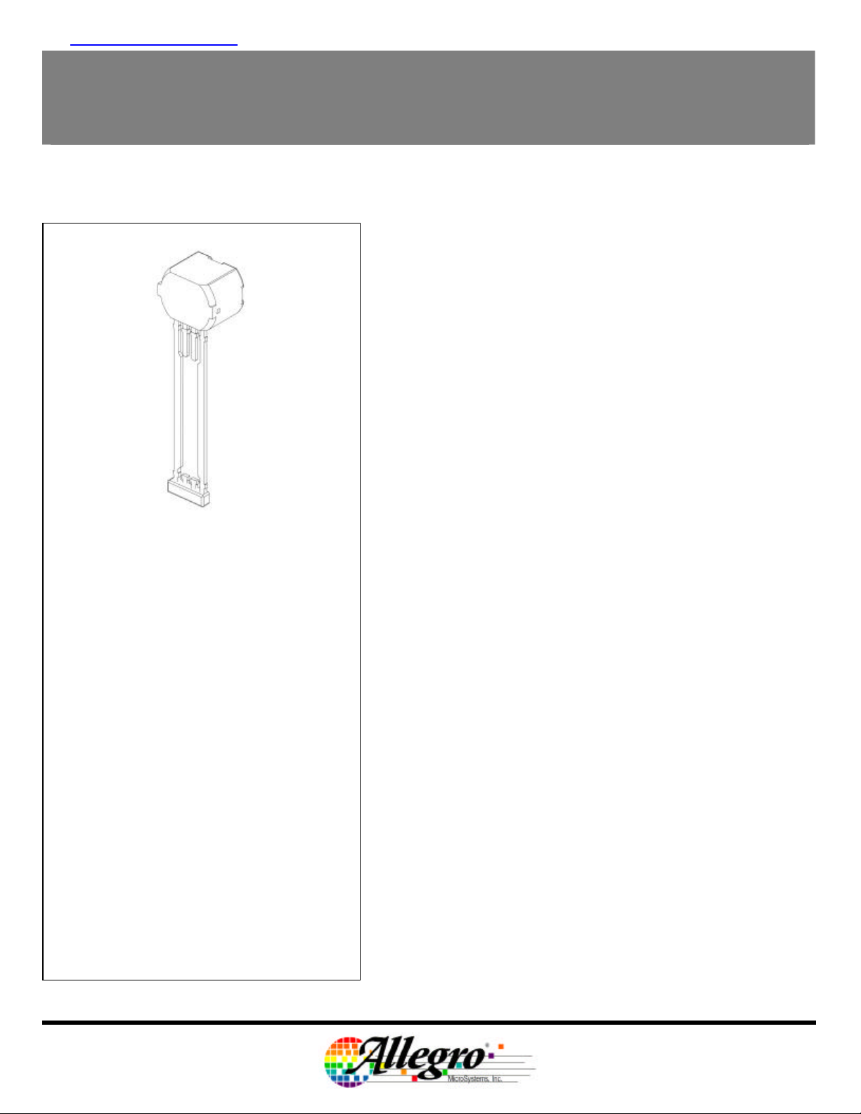
Pin 1: Supply
Pin 2: No connection
Pin 3: Test pin
Pin 4: Ground
Miniature Gear Tooth Sensor
The ATS645LSH is an optimized Hall effect sensing integrated
circuit and magnet combination that provides a user-friendly
solution for true zero-speed digital gear-tooth sensing in two-wire
applications. The sensor consists of a single-shot molded plastic
package that includes a samarium cobalt magnet, a pole piece, and
This small package can be easily assembled and used in
conjunction with a wide variety of gear shapes and sizes.
The integrated circuit incorporates a dual element Hall effect
sensor and signal processing that switches in response to
differential magnetic signals created by ferrous gear teeth. The
circuitry contains a sophisticated digital circuit to eliminate magnet
and system offsets and to achieve true zero speed operation (ref
U.S. Patent 5,917,320). A-D and D-A converters are used to adjust
the device gain at power up and to allow air gap independent
switching.
The regulated current output is configured for two wire
applications and the sensor is ideally suited for obtaining speed and
duty cycle in ABS and transmission application gear-tooth-based
configurations.
ABSOLUTE MAXIMUM RATINGS
Supply Voltage,
VCC . . . . . . . . . . . . . . . . . . . . . . . . . 26.5 V*
Reverse Supply Voltage,
VR . . . . . . . . . . . . . . . . . . . . . . . . . . . . –18 V
Operating Temperature Range,
TA . . . . . . . . . . . . . . . . . –40 °C to 150 °C*
Storage Temperature,
TS . . . . . . . . . . . . . . . . . . . . . . . . . . . 170 °C
Package Power Rating,
ϑJA . . . . . . . . . . . . . . . . . . . . . . . . 126 °C/W
Maximum Junction Temperature,
T
* Operation at increased supply voltages with external
circuitry is described in the Applications Information.
. . . . . . . . . . . . . . . . . . . . . 165 °C
Jmax
FEATURES
s Fully optimized differential digital gear tooth sensor
s Single chip sensing IC for high reliability
s Internal current regulator for 2 wire operation
s Small mechanical size (8 mm dia x 5.5 mm length)
s Air gap independent switch points
s Digital output representing gear profile
s Precise duty cycle signal with temperature
s Large operating air gaps
s Automatic Gain Control (AGC)
s Automatic Offset Adjustment circuit
s True zero speed operation
s Under-voltage lockout
s Wide operating voltage range
s Defined power-on state

ATS645LSH – Preliminary – Allegro Confidential
TRUE ZERO SPEED DIFFERENTIAL PEAK DETECTOR
CHARACTERISTICS
Valid over operating temperature range and Supply Voltage within specification unless otherwise noted.
Limits
Characteristics Symbol Test Conditions
Min. Typ. Max. Units
ELECTRICAL CHARACTERISTICS
Supply Voltage VCC Operating, TJ < 165°C 4.0 24 V
Under Voltage Lockout V
1
Supply Zener Clamp Voltage VZ IZT = 1 mA 28 32 - V
VCC 0 → 5 V - - <Vcc
CC(UV)
V
Min
Max Zener Pulse Current IZ t=20mS Pulse Mode - - 50 mA
Supply Zener Resistance RZ - 50 - Ω
Supply Current
ATS645LSH – I1
Supply Current
ATS645LSH – I2
ICC
Low Current State: Icc
High Current State: Icc
Low Current State: Icc
ICC
High Current State: Icc
4.0 6 8.0 mA
Low
12.0 14.0 16.0 mA
High
5.9 7 8.4 mA
Low
11.8 14.0 16.8 mA
High
POWER-ON STATE CHARACTERISTICS
Power-On State SPO VCC 0 → 5 V - Icc
2
Power-On Time t
on
Gear speed < 100 rpm - 1 2 ms
- -
High
OUTPUT STAGE
Icc
Output Current Slew Rate IR
à Icc
High
RS = 100 Ω, CS = 10 pF, 10 to 90%
Low
, Icc
Low
à Icc
High
,
10
mA/µs
1
The zener is tested using a pulse method and is designed for transient protection, continuous operation may destroy the device.
2
Power On Time is the time required to complete internal offset adjust. It does not include automatic gain control, which requires
three tooth valley transitions to complete and is therefore RPM dependent.
Revision 1.2; MHN; 07.Aug.02
Page 2 of 12
115 Northeast Cutoff, Box 15036
Worcester, Massachusetts 01615-0036 (508) 853-5000
Copyright © 1993, 1995 Allegro MicroSystems, Inc.

ATS645LSH – Preliminary – Allegro Confidential
TRUE ZERO SPEED DIFFERENTIAL PEAK DETECTOR
Operating Characteristics: Valid with Reference Target unless otherwise specified
Characteristics Symbol Test Conditions
Min. Typ. Max. Units
SWITCH POINT CHARACTERISTICS
Rotation Speed S
max
Using Reference Target over Operating
Air Gap Range
Analog Signal Bandwidth f-3db -3dB Point 20 40 KHz
1
Operate Point Bop
1
Release Point Brp
Icc
High
à Icc
Low
Positive Peak referenced, AG < AG
Icc
Low
à Icc
High
Negative Peak referenced, AG < AG
max
max
Calibration
Initial Calibration CI
Number of Rising Mechanical Edges for
Accurate Edge Detection
DAC Characteristics
Allowable User Induced
Differential Offset
Output switching only; may not meet
data sheet specifications
-60 60 G
Limits
0 8K RPM
- 100 150 mV
- 100 150 mV
3 Edges
SWITCH POINT DETAIL
Bop
Input
Differential
Signal
Device
Output
Current
Pin 3 Differential Signal (not magnetic signal)
1
Bop and Brp should be adjustable with metal mask changes, limits max air gap but improves vibration immunity.
Revision 1.2; MHN; 07.Aug.02
Page 3 of 12
Brp
115 Northeast Cutoff, Box 15036
Worcester, Massachusetts 01615-0036 (508) 853-5000
Copyright © 1993, 1995 Allegro MicroSystems, Inc.

ATS645LSH – Preliminary – Allegro Confidential
TRUE ZERO SPEED DIFFERENTIAL PEAK DETECTOR
Operating Characteristics:
Valid only if magnetic offset is within the Dynamic Offset Compensation DAC Range as specified above
Characteristics Symbol Test Conditions
Min. Typ. Max. Units
OPERATING CHARACTERISTICS: Using Reference Target and Valid Over Operating Temperature Range
1
Operational Air Gap Range Op
Switching Air Gap Range Op
MaxAG
Duty cycle within specification 0.5 2.75 mm
AG
Output Switching: Duty cycle Not in
Specification
Wobble < 0.5mm
Duty Cycle Variation DC
Typical value at 1.5mm air gap
37 53 57 %
Valid over operating air gap range
2
Operating Signal Range Sig
3
Minimum Operating Signal
Sig
Duty cycle within Specification
Wobble < 0.5mm
Output Switching: Duty Cycle Not in
Min
Specification
30 - 1000 G
20 - - G
Limits
3 - - mm
1
Operating air gap is dependent on the available magnetic field. The available field is target geometry and materiel
dependent and should be independently characterized. The field available from the reference target is given in the
reference gear parameter section of the datasheet
2
In order to remain in specification the magnetic signal must be larger than the minimum value specified, this includes the
effect of target wobble.
3
Duty cycle is not guaranteed to be in specification. Reference the Duty Cycle vs. Air Gap Over Temperature graph in
the typical operating characteristics section of this document.
Revision 1.2; MHN; 07.Aug.02
Page 4 of 12
115 Northeast Cutoff, Box 15036
Worcester, Massachusetts 01615-0036 (508) 853-5000
Copyright © 1993, 1995 Allegro MicroSystems, Inc.

ATS645LSH – Preliminary – Allegro Confidential
TRUE ZERO SPEED DIFFERENTIAL PEAK DETECTOR
Reference Gear Parameters
REFERENCE GEAR DIMENSIONS (60-0)
Diameter G
d
- 120 - mm
Thickness Gt - 6 - mm
Tooth Width Tw - 3 - mm
Valley Width V
w
- 3 - mm
Valley Depth Vd - 3 - mm
Materiel Low Carbon Steel
300
0.94mm
250
1.19mm
1.44mm
1.69mm
200
1.94mm
2.19mm
150
2.44mm
2.69mm
2.94mm
100
3.19mm
3.44mm
50
3.69mm
0
-50
Flux Density (Gauss)
-100
-150
-200
-250
-300
244 246 248 250 252 254 256 258 260 262
Flux Density vs. Position
Reference Target
Position (º)
Target Description:
Tooth Width: 3.25mm
Diameter: 120mm
Valley Width: 3.10mm
Tooth Thickness: 6mm
Valley Depth: 3mm
Revision 1.2; MHN; 07.Aug.02
Page 5 of 12
500
450
400
350
300
250
P-P [Gauss]
200
150
100
50
0
0.75 1 1.25 1.5 1.75 2 2.25 2.5 2.75 3 3.25 3.5 3.75
Reference Target Peak to Peak vs. Air Gap
Air Gap [mm]
115 Northeast Cutoff, Box 15036
Worcester, Massachusetts 01615-0036 (508) 853-5000
Copyright © 1993, 1995 Allegro MicroSystems, Inc.

ATS645LSH – Preliminary – Allegro Confidential
TRUE ZERO SPEED DIFFERENTIAL PEAK DETECTOR
Typical Operating Characteristics: Duty Cycle vs. Air Gap Over Temperature
65
60
Allegro MicroSystems, Inc. Standard Production 60-0 Target
Typical @ 25ºC
Typical @ 150ºC
Typical @ -40ºC
55
50
Duty Cycle (%)
45
40
35
0.5 0.75 1 1.25 1.5 1.75 2 2.25 2.5 2.75 3 3.25
Figure #1: Duty Cycle vs. Air Gap Over Tem perature with Reference Target and Orientation Given in Figure #2
Duty Cycle vs. Air Gap
ATS645LSH @ 1000RPM
Air Gap (mm)
ROTATION RIGHT is CW from pin 4 to pin 1
Figure #2: Sensor Orientation and Direction of Rotation of Reference Target for Duty Cycle
Graph in Figure #1
Revision 1.2; MHN; 07.Aug.02
Page 6 of 12
115 Northeast Cutoff, Box 15036
Worcester, Massachusetts 01615-0036 (508) 853-5000
Copyright © 1993, 1995 Allegro MicroSystems, Inc.

ATS645LSH – Preliminary – Allegro Confidential
TRUE ZERO SPEED DIFFERENTIAL PEAK DETECTOR
SENSOR DESCRIPTION
Assembly Description:
The ATS645LSH true zero speed gear tooth sensor is a Hall IC/magnet configuration that is fully optimized to provide
digital detection of gear tooth edges. This sensor is integrally molded into a plastic body that has been optimized for size,
ease of assembly, and manufacturability. High operating temperature materials are used in all aspects of construction.
Sensing Technology:
The gear tooth sensor sub-assembly contains a single-chip differential Hall effect sensor IC, a Samarium Cobalt magnet,
and a flat ferrous pole piece. The Hall IC consists of 2 Hall elements spaced 1.5 mm apart that measure the magnetic
gradient created by the passing of a ferrous object. The two elements measure the magnetic gradient and convert it to an
analog voltage that is then processed to provide a digital output signal.
Revision 1.2; MHN; 07.Aug.02
Page 7 of 12
115 Northeast Cutoff, Box 15036
Worcester, Massachusetts 01615-0036 (508) 853-5000
Copyright © 1993, 1995 Allegro MicroSystems, Inc.

ATS645LSH – Preliminary – Allegro Confidential
TRUE ZERO SPEED DIFFERENTIAL PEAK DETECTOR
Transient Performance per ISO 7637-1
at TA = 23 ±5°C
(Tested at Allegro test facility – for engineering reference only)
Performance Class at Test Level
Pulse No. Test
1 Inductive turn off (negative) - - - C
2 Inductive turn off (positive) - - - A
3a Capacitive/inductive coupling (neg) - - - A
3b Capacitive/inductive coupling (pos) - - - A
4 Reverse battery - - - A
5 Load dumb A C C E
6 Ignition coil disconnect - - C E
7 Field decay (negative) - - - C
UA = 13.5V for pulses 1, 2, 3a, 3b, 5, 6, 7 and 12V for pulse 4.
Test Circuit #1
PCB Ouline by Dashed Line
Icc
Pin #1
Pin #2
Pin #3
Pins #2 and #3 Floating
Power supply voltage transients, or device output short circuits,
may be caused by faulty connectors, crimped wiring
harnesses, or service errors. The prevent catastrophic failure,
internal protection against over-voltage, reverse voltage, and
output overloads have been incorporated to meet the
automotive 12 volt system protection requirements of ISO
DP7637/1. A series-blocking diode or current -limiting resistor
is required in order to survive pulse number six.
645
Pin #4
Transient & EMC test circuit
0.01uF
ECU
100Ohm
V
EMC
A – All functions of a device perform as designed during and
after the exposure.
B – All functions of a device perform as designed during
exposure; however, one or more of them may go beyond the
specified limit tolerance. All functions return automatically to
within normal limits after exposure is removed. Memory must
remain Class A.
C – One or more functions of the device do not perform as
designed during exposure but return automatically to normal
operation after exposure is removed.
D – One or more functions of the device do not perform as
designed during exposure and do not return to normal
operation until exposure is removed and the device is reset by
simple “ operator” action.
E – One or more functions of the device do not perform as
designed during and after the exposure and cannot be
returned to proper operation without repairing or replacing the
device.
Revision 1.2; MHN; 07.Aug.02
Page 8 of 12
I II III IV
Performance Class Definitions
(for transient performance and EMC performance)
115 Northeast Cutoff, Box 15036
Worcester, Massachusetts 01615-0036 (508) 853-5000
Copyright © 1993, 1995 Allegro MicroSystems, Inc.

Performance Class at Test Level
Frequency Band
Performance Class at Test Level
Frequency Band
Performance Class at Test Level
Frequency Band
Test severity level
I = 50 V/m
II = 100 V/m
III = 150 V/m
IV = 200 V/m
Test severity level
I = 25 mA
II = 50 mA
III = 75 mA
IV = 100 mA
Test severity level
I = 100 mW
II = 200 mW
III = 300 mW
IV = 400 mW
V = 500 mW
ATS645LSH – Preliminary – Allegro Confidential
TRUE ZERO SPEED DIFFERENTIAL PEAK DETECTOR
ELECTROMAGNETIC COMPATIBILITY (EMC) PERFORMANCE
at TA = 23 ±5°C
(Tested at Allegro test facility – for engineering reference only)
TEM Cell Performance per ISO 11452-3
(MHz) I II III IV
F1 (0.01 to 10)
F2 (0 to 30)
F3 (30 to 80)
F4 (80 to 200)
(MHz) I II III IV
F1 (1 to 10)
F2 (10 to 30)
F3 (30 to 80)
F4 (80 to 200)
F5 (200 to 400)
(MHz)
F1 (1 to 10)
F2 (10 to 30)
F3 (30 to 80)
F4 (80 to 200)
F5 (200 to 400)
– – –
– – –
– – –
–
A B B
BCI per ISO 11452-4
– – –
– – –
– – –
– – –
– – –
Direct RF per ISO 11452-7
I II III IV V
A
A
A
A
A
A
A
A
Revision 1.2; MHN; 07.Aug.02
Page 9 of 12
115 Northeast Cutoff, Box 15036
Worcester, Massachusetts 01615-0036 (508) 853-5000
Copyright © 1993, 1995 Allegro MicroSystems, Inc.

ATS645LSH – Preliminary – Allegro Confidential
TRUE ZERO SPEED DIFFERENTIAL PEAK DETECTOR
MECHANICAL INFORMATION
Component Material Function Value
Sensor Package
Material
Leads Copper, 0.016” dia, 0.050” spacing
Lead Coating Solder, Tin / Lead 90/102
1
Temperature excursions of up to 225°C for 2 minutes or less are permitted.
2
Industry accepted soldering techniques are acceptable for this sub-assembly as long as the indicated maximum
temperatures for each component are not exceeded.
Thermoset Epoxy Max. Temperature 170°C1
DEVICE QUALIFICATION PROGRAM
Test Name Test Conditions Test Length # of Lots Sample / lot
High Temperature
Operating Life
High Temperature Bake
Temperature Humidity
Bias
Autoclave AEC-Q100 #6 (JA102) 96 hrs 1 77
Temperature Cycling AEC-Q100 #7(JA104) 500 cycles 1 77
ESD
Early Life Failure Rate
AEC-Q100 #2 (JA108)
Ta = 150°C, Tj = 165°C
AEC-Q100 #3 (JA103)
Ta = 170°C
AEC-Q100 #5 (JA101)
85°C/85%RH
AEC-Q100 #20 (AEC-Q100002, AEC-Q100-003)
AEC-Q100 #25 (AEC-Q100-
008)
408 hrs 1 77
1000 hrs 1 77
1008 hrs 1 77
- 1 3/model/step
150°C/24 hrs 1 800
-65°C to +160°C, 30 sec.
transition, 30 minute dwell
Passes ±6kV all pin
combinations: Human
Body Model
Comments
Revision 1.2; MHN; 07.Aug.02
Page 10 of 12
115 Northeast Cutoff, Box 15036
Worcester, Massachusetts 01615-0036 (508) 853-5000
Copyright © 1993, 1995 Allegro MicroSystems, Inc.

TRUE ZERO SPEED DIFFERENTIAL PEAK DETECTOR
Functional block diagram
ATS645LSH – Preliminary – Allegro Confidential
Vcc/Output
Auto Offset
Control
Track DAC
Hall AMP AGC
Offset DAC
+
AGC DAC
Peak Hold
Typical Application Circuit
INTERNAL
REGURATOR
Test signals
V
Neg
Test Pin
Revision 1.2; MHN; 07.Aug.02
Page 11 of 12
PCB Ouline by Dashed Line
Pin #1
Pin #2
Pin #3
645
Pin #4
Pins #2 and #3 Floating
0.01uF
Icc
ECU
100Ohm
115 Northeast Cutoff, Box 15036
Worcester, Massachusetts 01615-0036 (508) 853-5000
Copyright © 1993, 1995 Allegro MicroSystems, Inc.
V
Supply

ATS645LSH – Preliminary – Allegro Confidential
TRUE ZERO SPEED DIFFERENTIAL PEAK DETECTOR
SENSOR PACKAGE
LSH PACKAGE
REFERENCE DIMENSIONS ONLY
Revision 1.2; MHN; 07.Aug.02
Page 12 of 12
115 Northeast Cutoff, Box 15036
Worcester, Massachusetts 01615-0036 (508) 853-5000
Copyright © 1993, 1995 Allegro MicroSystems, Inc.
 Loading...