

查询ATS625LSG供应商
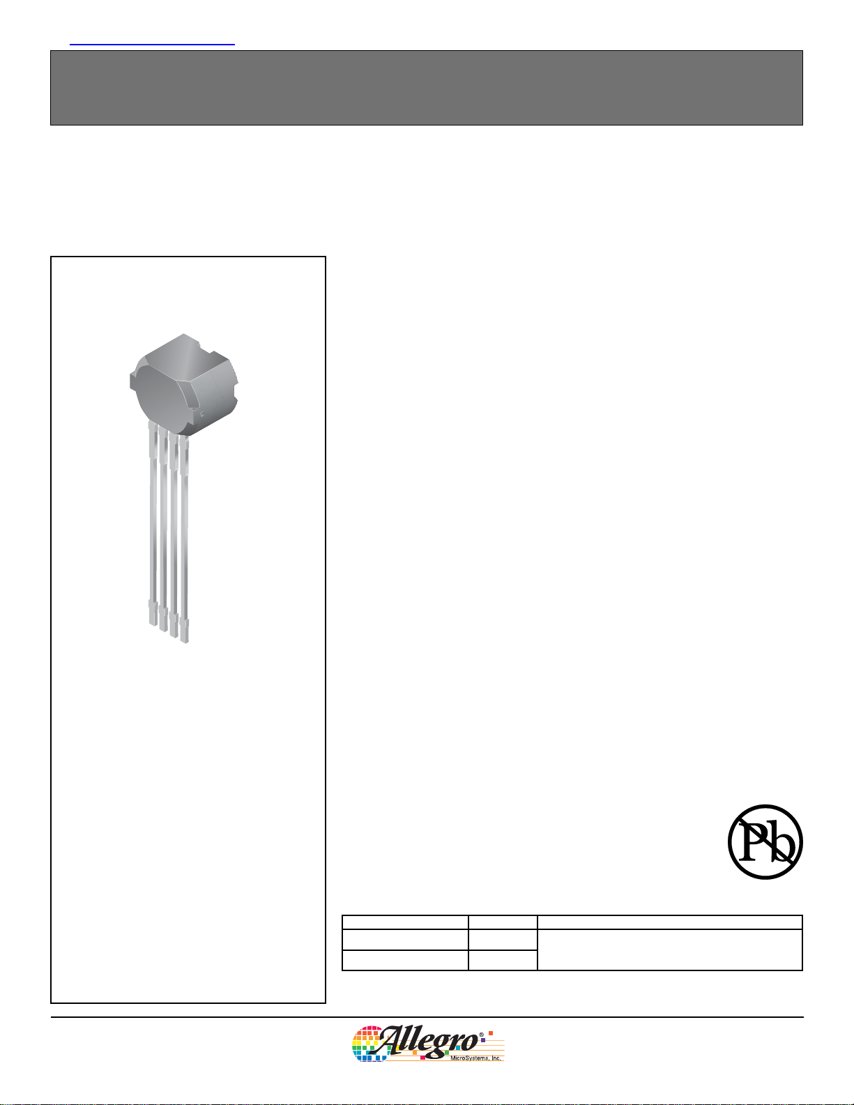
Package SG, 4-pin Through Hole
ATS625LSG
True Zero-Speed Low-Jitter
High Accuracy Gear Tooth Sensor
The ATS625 true zero-speed gear tooth sensor is an optimized Hall IC and magnet
configuration packaged in a molded module that provides a manufacturer-friendly
solution for digital gear tooth sensing applications. The sensor assembly consists
of an over-molded package that holds together a samarium cobalt magnet, a
pole piece concentrator, and a true zero-speed Hall IC that has been optimized
to the magnetic circuit. This small package can be easily assembled and used in
conjunction with gears of various shapes and sizes.
The sensor incorporates a dual-element Hall IC that switches in response to
differential magnetic signals created by a ferrous target. Digital processing of the
analog signal provides zero-speed performance independent of air gap as well
as dynamic adaptation of device performance to the typical operating conditions
found in automotive applications (reduced vibration sensitivity). High-resolution
peak detecting DACs are used to set the adaptive switching thresholds of the
device. Switchpoint hysteresis reduces the negative effects of any anomalies in the
magnetic signal associated with the targets used in many automotive applications.
This sensor system is optimized for crank applications that utilize targets that
possess signature regions.
1
2
3
4
1. VCC
2. VOUT
3. AUX
4. GND
AB SO LUTE MAX I MUM RAT INGS
Supply Voltage*, VCC.......................................26.5 V
Reverse-Supply Voltage, V
Reverse-Supply Current, I
Reverse-Output Voltage, V
Continuous Output Current, I
Output Sink Current, I
Operating Temperature
Ambient, T
Maximum Junction, T
Maximum Junction ≤100 hr, T
Storage Temperature, T
*See the Power Derating section.
OUT
, Range L................–40ºC to 150ºC
A
........................–18 V
RCC
........................50 mA
RCC
.....................–0.5 V
ROUT
...................25 mA
OUT
............................. 10 mA
........................165ºC
J(max)
.................. –65ºC to 170ºC
S
J(max100)
......180ºC
TheATS625 is provided in a 4-pin SIP. The Pb (lead) free option, available by
special request, has a 100% matte tin plated leadframe.
Features and Benefits
Highly repeatable over operating temperature range
Tight timing accuracy over operating temperature range
True zero-speed operation
Air-gap–independent switchpoints
Vibration immunity
Large operating air gaps
Defined power-on state
Wide operating voltage range
Digital output representing target profile
Single-chip sensing IC for high reliability
Small mechanical size
Optimized Hall IC magnetic system
Fast start-up
AGC and reference adjust circuit
Undervoltage lockout
Use the following complete part numbers when ordering:
Part Number Pb-free Packing
ATS625LSGTN –
ATS625LSGTN-T Yes
1
Contact Allegro for additional packing options.
2
Available by special request only.
2
Tape and Reel 13-in. 800 pcs./reel
1
ATS625LSG-DS, Rev. 1
Allegro MicroSystems, Inc.
115 Northeast Cutoff, Box 15036
Worcester, Massachusetts 01615-0036 (508) 853-5000
www.allegromicro.com

V+
0.1 F
C
BYPASS
VCC
ATS625LSG
True Zero-Speed Low-Jitter High Accuracy Gear Tooth Sensor
Functional Block Diagram
Voltage
Regulator
Threshold
Comparator
Threshold
Logic
Hall
Amp
Automatic
Gain
Control
PPeak
PDAC
V
PROC
NDAC
NPeak
Reference
Generator
PThresh
NThresh
GND
(Recommended)
AUX
Current
Limit
Output
Transistor
VOUT
ATS625LSG-DS, Rev. 1
Allegro MicroSystems, Inc.
115 Northeast Cutoff, Box 15036
Worcester, Massachusetts 01615-0036 (508) 853-5000
www.allegromicro.com
2

ATS625LSG
True Zero-Speed Low-Jitter High Accuracy Gear Tooth Sensor
Operating Characteristics Valid at T
= –40°C to 150°C, TJ ≤ T
A
operating parameters: VCC = 12 V and TA = 25°C
Characteristic Symbol Test Conditions Min. Typ. Max. Units
ELECTRICAL CHARACTERISTICS
Supply Voltage V
Undervoltage Lockout V
Reverse Supply Current I
Supply Zener Clamp Voltage
Supply Zener Current
1
2
Supply Current I
CC
CCUV
RCC
V
Z
I
Z
CC
POWER-ON CHARACTERISTICS
Power-On State S
Power-On Time t
PO
PO
OUTPUT STAGE
Low Output Voltage V
Output Current Limit I
Output Leakage Current I
Output Rise Time t
Output Fall Time t
OUT(SAT)ISINK
OUT(LIM)VOUT
OUT(OFF)
r
f
SWITCHPOINT CHARACTERISTICS
, over full range of AG, unless otherwise noted; typical
J(max)
Operating; TJ < T
Jmax
4.0 – 24 V
– – < V
CC(min)
V
VCC = –18 V – – –10 mA
ICC = 17 mA 28 – – V
VS = 28 V – – 17 mA
Output OFF – 8.5 14 mA
Output ON – 8.5 14 mA
– High – V
Gear Speed < 100 RPM; VCC > VCC min – – 200 µs
= 20 mA, Output = ON – 200 450 mV
= 12 V, TJ < T
Output = OFF, V
Jmax
= 24 V – – 10 µA
OUT
25 45 70 mA
RL = 500 Ω, CL = 10 pF – 1.0 2 µs
RL = 500 Ω, CL = 10 pF – 0.6 2 µs
Speed S Reference target 60+2 0 – 12000 rpm
Bandwidth BW Corresponds to switching frequency – 3 dB – 20 – kHz
Operate Point B
Release Point B
% of peak-to-peak signal, AG < AG
OP
BIN transitioning from LOW to HIGH
% of peak-to-peak signal, AG < AG
RP
BIN transitioning from HIGH to LOW
max
max
;
;
–60 – %
–40 – %
CALIBRATION
Initial Calibration
3
Cal
Start-up – 1 6 edges
PO
Calibration Update Cal Running mode operation continuous –
Continued on the next page...
Allegro MicroSystems, Inc.
ATS625LSG-DS, Rev. 1
115 Northeast Cutoff, Box 15036
Worcester, Massachusetts 01615-0036 (508) 853-5000
www.allegromicro.com
3

ATS625LSG
True Zero-Speed Low-Jitter High Accuracy Gear Tooth Sensor
Operating Characteristics, continued Valid at T
= –40°C to 150°C, TJ ≤ T
A
, over full range of AG, unless otherwise noted;
J(max)
typical operating parameters: VCC = 12 V and TA = 25°C
Characteristic Symbol Test Conditions Min. Typ. Max. Units
OPERATING CHARACTERISTICS with 60+2 reference target
Operational Air Gap AG
Relative Timing Accuracy, Sequential Mechanical Rising Edges
Relative Timing Accuracy, Sequential Mechanical Falling Edges
Relative Timing Accuracy, Signature Mechanical Rising Edge
4
Relative Timing Accuracy, Signature Mechanical Falling Edge
5
Relative Repeatability, Sequential
Rising and Falling Edges
Operating Signal
1
Test condition is I
2
Upper limit is I
3
Power-on speed ≤ 200 rpm. Refer to the Sensor Description section for information on start-up behavior.
4
Detection accuracy of the update algorithm for the first rising mechanical edge following a signature region can be adversely affected by the magnetic
bias of the signature region. Please consult with Allegro field applications engineering for aid with assessment of specific target geometries.
5
Detection accuracy of the update algorithm for the falling edge of the signature region is highly dependent upon specific target geometry. Please consult
with Allegro field applications engineering for aid with assessment of specific target geometries.
6
The repeatability specification is based on statistical evaluation of a sample population.
7
Peak-to-peak magnetic flux strength required at Hall elements for complying with operational characteristics.
7
CC(max)
CC(max)
6
+ 3 mA.
+ 3 mA.
ERR
ERR
ERR
ERR
T
B
Measured from sensor branded face to
target tooth
Relative to measurement taken at
RR
AG = 1.5 mm
Relative to measurement taken at
FF
AG = 1.5 mm
Relative to measurement taken at
SIGR
AG = 1.5 mm
Relative to measurement taken at
SIGF
AG = 1.5 mm
360° Repeatability, 1000 edges; peak-peak
sinusoidal signal with B
θE
PEAK
6° period
AG
IN
< AG < AG
(min)
(max)
≥ B
IN(min)
and
0.5 – 2.5 mm
– – ±0.4 deg.
– – ±0.4 deg.
– – ±0.4 deg.
– – ±1.5 deg.
– – 0.08 deg.
60 – – G
ATS625LSG-DS, Rev. 1
Allegro MicroSystems, Inc.
115 Northeast Cutoff, Box 15036
Worcester, Massachusetts 01615-0036 (508) 853-5000
www.allegromicro.com
4
ATS625LSG
True Zero-Speed Low-Jitter High Accuracy Gear Tooth Sensor
Reference Target (Gear) Information
REFERENCE TARGET 60+2
Characteristics Symbol Test Conditions Typ. Units Symbol Key
Outside Diameter D
Face Width F
Circular Tooth Length t
Signature Region Circular Tooth Length
Circular Valley Length t
Tooth Whole Depth h
Material Low Carbon Steel – –
t
SIG
Outside diameter of target
o
Breadth of tooth, with respect
to sensor
Length of tooth, with respect
to sensor; measured at D
Length of signature tooth,
with respect to sensor; measured at D
Length of valley, with respect
v
to sensor; measured at D
t
o
Pin 4
120 mm
6mm
3mm
o
15 mm
3mm
o
3mm
Branded Face
of Sensor
t,t
Air Gap
Signature Region
SIG
Ø
D
O
V
t
F
h
t
Pin 1
Branded Face
of Sensor
Reference Target
60+2
Figure 1. Configuration with Spur Gear Reference Target
For the generation of adequate magnetic field levels, the following recommendations should be followed in the design and
specification of targets:
• 2 mm < tooth width, t < 4 mm
• Valley width, tv > 2 mm
• Valley depth, ht > 2 mm
• Tooth thickness, F ≥ 3 mm
• Target material must be low carbon steel
ATS625LSG-DS, Rev. 1
Although these parameters apply to targets of traditional
geometry (radially oriented teeth with radial sensing, shown in
figure 1), they also can be applied in applications using stamped
targets (an aperture or rim gap punched out of the target mate-
rial) and axial sensing. For stamped geometries with axial sens-
ing, the valley depth, ht, is intrinsically infinite, so the criteria for
tooth width, t, valley width, tv, tooth material thickness, F, and
material specification need only be considered for reference. For
example, F can now be < 3 mm.
Allegro MicroSystems, Inc.
115 Northeast Cutoff, Box 15036
Worcester, Massachusetts 01615-0036 (508) 853-5000
www.allegromicro.com
5
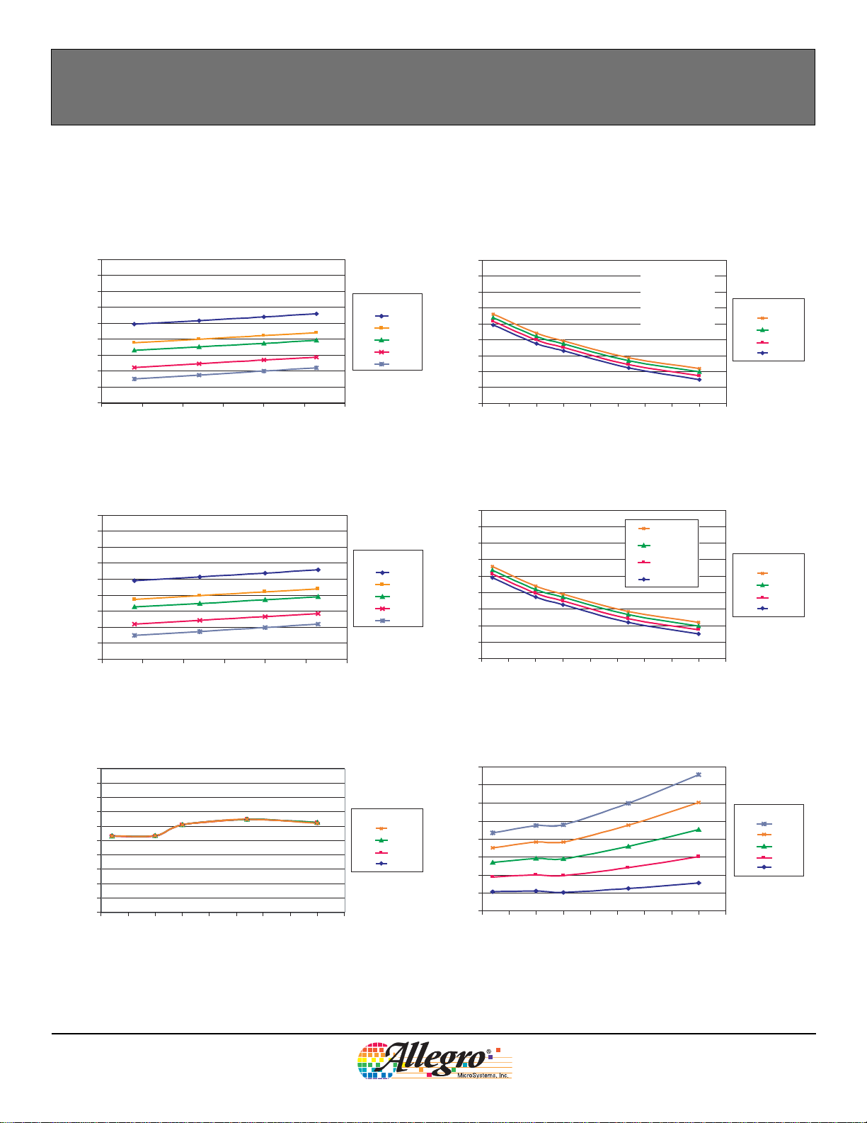
True Zero-Speed Low-Jitter High Accuracy Gear Tooth Sensor
I
Versus V
CC(ON)
14
13
12
11
10
9
8
Current (mA)
7
6
5
0 5 10 15 20 25 30
Voltage (V)
CC
ATS625LSG
Characteristic Data: Electrical
14
13
TA (°C)
-40
0
25
85
150
12
11
10
9
8
Current (mA)
7
6
5
-50 -25 0 25 50 75 100 125 150 175
I
Versus T
CC(ON)
Temperature (°C)
A
Vcc = 26.5V
Vcc = 20V
Vcc = 12V
Vcc = 4V
(V)
V
CC
26.5
20.0
12.0
4.0
I
Versus V
CC(OFF)
14
13
12
11
10
9
Current (mA)
8
7
6
5
0 5 10 15 20 25 30
CC
Voltage (V)
I
10
8
6
4
2
0
-2
Current (uA)
-4
-6
-8
-10
-50 -25 0 25 50 75 100 125 150 175
OUT(OFF)
Versus T
A
Temperature (°C)
TA (°C)
V
OUT
150
(V)
26.5
20.0
12.0
4.0
-40
I
Versus T
CC(OFF)
14
13
12
11
0
25
85
10
9
8
Current (mA)
7
6
5
-50 -25 0 25 50 75 100 125 150 175
A
Vcc = 24V
Vcc = 20V
Vcc = 12V
Vcc = 4V
VCC (V)
24.0
20.0
12.0
4.0
Temperature (°C)
V
400
350
300
250
200
150
Voltage (mV)
100
50
0
-50 -25 0 25 50 75 100 125 150 175
Temperature (°C)
OUT(SAT)
Versus T
A
I
(mA)
OUT
25
20
15
10
5
ATS625LSG-DS, Rev. 1
Allegro MicroSystems, Inc.
115 Northeast Cutoff, Box 15036
Worcester, Massachusetts 01615-0036 (508) 853-5000
www.allegromicro.com
6
ATS625LSG
True Zero-Speed Low-Jitter High Accuracy Gear Tooth Sensor
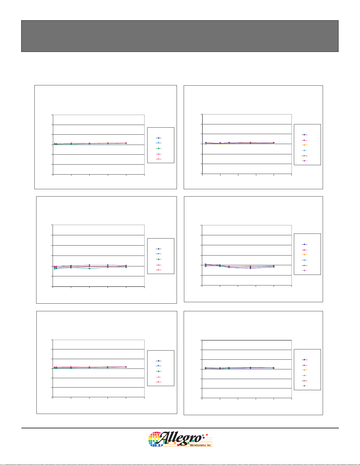
Characteristic Data: Relative Timing Accuracy
Relative Timing Accuracy Versus Speed
Signature Tooth Rising Edge
0.5 mm Air Gap
1.5
1.0
0.5
0.0
-0.5
Edge Position (°)
-1.0
-1.5
500 1000 1500 2000 2500
0
Target Speed, S (rpm)
Relative Timing Accuracy Versus Speed
Signature Tooth Falling Edge
0.5 mm Air Gap
1.5
1.0
0.5
0.0
-0.5
Edge Position (°)
-1.0
-1.5
0 500 1000 1500 2000 2500
Target Speed, S (rpm)
TA (°C)
–40
150
TA (°C)
–40
150
Relative Timing Accuracy Versus Ambient
Signature Tooth Rising Edge
0.5 mm Air Gap
1.5
1.0
0.5
0
25
85
0.0
-0.5
Edge Position (°)
-1.0
-1.5
-50 0 50 100 150 200
S (rpm)
50
100
500
1000
1500
2000
Tem perature, TA (°C)
Relative Timing Accuracy Versus Ambient
Signature Tooth Falling Edge
0.5 mm Air Gap
1.5
1.0
0.5
0
25
85
0.0
-0.5
Edge Position (°)
-1.0
-1.5
-50 0 50 100 150 200
Tem perature, TA (°C)
S (rpm)
50
100
500
1000
1500
2000
Relative Timing Accuracy Versus Speed
Rising Edge Follow ing Signature Tooth
1.5
1.0
0.5
0.0
-0.5
Edge Position (°)
-1.0
-1.5
0 500 1000 1500 2000 2500
ATS625LSG-DS, Rev. 1
0.5 mm Air Gap
Target Speed, S (rpm)
TA (°C)
–40
150
Relative Timing Accuracy Versus Ambient
Rising Edge Follow ing Signature Tooth
0.5 mm Air Gap
1.5
1.0
0.5
0
25
85
0.0
-0.5
Edge Position (°)
-1.0
-1.5
-50 0 50 100 150 200
Tem perature, TA (°C)
Allegro MicroSystems, Inc.
115 Northeast Cutoff, Box 15036
Worcester, Massachusetts 01615-0036 (508) 853-5000
www.allegromicro.com
S (rpm)
50
100
500
1000
1500
2000
7

ATS625LSG
True Zero-Speed Low-Jitter High Accuracy Gear Tooth Sensor
Relative Timing Accuracy Versus Speed
Signature Tooth Rising Edge
2.5 mm Air Gap
1.5
1.0
0.5
0.0
-0.5
Edge Position (°)
-1.0
-1.5
500 1000 1500 2000 2500
0
Target Speed, S (rpm)
Relative Timing Accuracy Versus Speed
Signature Tooth Falling Edge
2.5 mm Air Gap
1.5
1.0
0.5
0.0
-0.5
Edge Position (°)
-1.0
-1.5
0 500 1000 1500 2000 2500
Target Speed, S (rpm)
TA (°C)
–40
150
TA (°C)
–40
150
Relative Timing Accuracy Versus Ambient
Signature Tooth Rising Edge
2.5 mm Air Gap
1.5
1.0
0.5
0
25
85
0.0
-0.5
Edge Position (°)
-1.0
-1.5
-50 0 50 100 150 200
S (rpm)
50
100
500
1000
1500
2000
Tem perature, TA (°C)
Relative Timing Accuracy Versus Ambient
Signature Tooth Falling Edge
2.5 mm Air Gap
1.5
1.0
0.5
0
25
85
0.0
-0.5
Edge Position (°)
-1.0
-1.5
-50 0 50 100 150 200
Tem perature, TA (°C)
S (rpm)
50
100
500
1000
1500
2000
Relative Timing Accuracy Versus Speed
Rising Edge Follow ing Signature Tooth
1.5
1.0
0.5
0.0
-0.5
Edge Position (°)
-1.0
-1.5
0 500 1000 1500 2000 2500
ATS625LSG-DS, Rev. 1
2.5 mm Air Gap
Target Speed, S (rpm)
TA (°C)
–40
150
Relative Timing Accuracy Versus Ambient
Rising Edge Follow ing Signature Tooth
2.5 mm Air Gap
1.5
1.0
0.5
0
25
85
0.0
-0.5
Edge Position (°)
-1.0
-1.5
-50 0 50 100 150 200
Tem perature, TA (°C)
Allegro MicroSystems, Inc.
115 Northeast Cutoff, Box 15036
Worcester, Massachusetts 01615-0036 (508) 853-5000
www.allegromicro.com
S (rpm)
50
100
500
1000
1500
2000
8

ATS625LSG
True Zero-Speed Low-Jitter High Accuracy Gear Tooth Sensor
Relative Timing Accuracy Versus Air Gap
Signature Tooth R ising Edge
= –40, 0, 25, 85, 150 (°C)
T
A
S = 50, 100, 500, 1000, 1500, 2000 (rpm)
2.0
1.5
1.0
0.5
0.0
-0.5
-1.0
Edge Position (°)
-1.5
0.0 0.5 1.0 1.5 2.0 2.5 3.0
Air Gap (mm)
2.0
1.5
1.0
0.5
0.0
-0.5
Edge Position (°)
-1.0
-1.5
0 0.5 1.0 1.5 2.0 2.5 3.0
Relative Timing Accuracy Versus Air Gap
2.0
1.5
1.0
0.5
0.0
-0.5
-1.0
Edge Position (°)
-1.5
0.0 0.5 1.0 1.5 2.0 2.5 3.0
Relative Timing Accuracy Versus Air Gap
Rising Edge Following Signature Tooth
TA = –40, 0, 25, 85, 150 (°C)
S = 50, 100, 500, 1000, 1500, 2000 (rpm)
Air Gap (mm)
Signature Tooth Fa lling Edge
TA = –40, 0, 25, 85, 150 (°C)
S = 50, 100, 500, 1000, 1500, 2000 (rpm)
Air Gap (mm)
ATS625LSG-DS, Rev. 1
Characteristic Data: Repeatability
360° Repeatability Versus Air Gap
Sequential Tooth Falling Edge
S = 1000 rpm
0.25
(°C)
T
0.20
0.15
0.10
Repeatabilty (°)
0.05
0
0 1.0 2.0 3.0 4.0
A
–40
25
150
Air Gap (mm)
Allegro MicroSystems, Inc.
115 Northeast Cutoff, Box 15036
Worcester, Massachusetts 01615-0036 (508) 853-5000
www.allegromicro.com
9

ATS625LSG
(
)(
)
True Zero-Speed Low-Jitter High Accuracy Gear Tooth Sensor
Sensor Description
Assembly Description
The ATS625LSG true zero-speed gear tooth sensor is a combined Hall IC-magnet configuration that is fully optimized to
provide digital detection of gear tooth edges. This sensor is
integrally molded into a plastic body that has been optimized for
size, ease of assembly, and manufacturability. High operating
temperature materials are used in all aspects of construction.
Sensing Technology
The gear tooth sensor contains a single-chip differential Hall
effect sensor IC, a 4-pin leadframe, a samarium cobalt magnet,
and a flat ferrous pole piece. The Hall IC consists of two Hall
elements spaced 2.2 mm apart, and each independently measures
Target (Gear)
Element Pitch
Hall Element 2
Dual-Element
Hall Effect Device
Pin n >1 Side
Figure 2. Device Cross Section. Relative motion of the target is detected
by the dual Hall elements mounted on the Hall IC. This view is from the
side opposite the pins.
South Pole
North Pole
Hall Element 1
Hall IC
Pole Piece
(Concentrator)
Back-biasing Magnet
Plastic
Pin 1 Side
the magnetic gradient created by the passing of a ferrous object.
This is illustrated in figures 2 and 3. The differential output of
the two elements is converted to a digital signal that is processed
to provide the digital output.
Switching Description
After proper power is applied to the component, the sensor is
then capable of providing digital information that is representative of the profile of a rotating gear, as illustrated in figure 4.
No additional optimization is needed and minimal processing
circuitry is required. This ease of use reduces design time and
incremental assembly costs for most applications.
Rotating Target
1
4
Figure 3. This left-to-right (pin 1 to pin 4) direction of target rotation
results in a high output signal when a tooth of the target gear is centered
over the face of the sensor. A right-to-left (pin 4 to pin 1) rotation inverts
the output signal polarity.
Branded Face
of Sensor
Target
Mechanical Profile
Target
Magnetic Profile
Sensor Output
Switch State
Sensor Output
Electrical Profile
Target Motion from
Pin 1 to Pin 4
Sensor Output
Electrical Profile
Target Motion from
Pin 4 to Pin 1
Figure 4. The magnetic profile reflects the geometry of the target, allowing the device to present an accurate digital output response.
ATS625LSG-DS, Rev. 1
B+
B
IN
On Off On Off On Off On Off On OffOn OffOn OffOn Off
V+
V
OUT
V+
V
OUT
Signature Tooth
Allegro MicroSystems, Inc.
115 Northeast Cutoff, Box 15036
Worcester, Massachusetts 01615-0036 (508) 853-5000
www.allegromicro.com
10

ATS625LSG
True Zero-Speed Low-Jitter High Accuracy Gear Tooth Sensor
Undervoltage Lockout
When the supply voltage falls below the undervoltage lockout
level, V
, the device switches to the OFF state. The device
CCUV
remains in that state until the voltage level is restored to to the
VCC operating range. Changes in the target magnetic profile
have no effect until voltage is restored. This prevents false signals caused by undervoltage conditions from propagating to the
output of the sensor.
Power Supply Protection
The device contains an on-chip regulator and can operate over
a wide range of supply voltage levels. For applications using an
unregulated power supply, transient protection must be added
externally. For applications using a regulated supply line, EMI
and RFI protection may still be required. The circuit shown in
V
S
C
BYPASS
0.1 µF
3
figure 5 is the basic configuration required for proper device
operation. Contact Allegro field applications engineering for
information on the circuitry required for compliance to various
EMC specifications.
Internal Electronics
The ATS625LSG contains a self-calibrating Hall effect IC
that possesses two Hall elements, a temperature compensated
amplifier and offset cancellation circuitry. The IC also contains
a voltage regulator that provides supply noise rejection over the
operating voltage range. The Hall transducers and the electronics are integrated on the same silicon substrate by a proprietary
BiCMOS process. Changes in temperature do not greatly affect
this device due to the stable amplifier design and the offset rejection circuitry.
1
VCC
ATS625
2
VOUTAUX
R
PU
Sensor Output
ATS625LSG-DS, Rev. 1
GND
4
Figure 5. Power Supply Protection Typical Circuit
Allegro MicroSystems, Inc.
115 Northeast Cutoff, Box 15036
Worcester, Massachusetts 01615-0036 (508) 853-5000
www.allegromicro.com
11

ATS625LSG
True Zero-Speed Low-Jitter High Accuracy Gear Tooth Sensor
Sensor Operation Description
Power-On State
At power-on, the device is guaranteed to initialize in the OFF
state, with V
OUT
high.
First Edge Detection
The device uses the first two mechanical edges to synchronize
with the target features (tooth or valley) and direction of rotation
of the target. The device is synchonized by the third edge. The
actual behavior is affected by: target rotation direction relative to
Sensor
Pin 4 Side
Target Mechanical Profile
Target Magnetic Profile
(A) Target relative movement
as shown in figure 3. Output
signal is high over the tooth.
Sensor Output, V
(Start-up over rising edge)
OUT
(Start-up over valley)
(Start-up over tooth)
the, target feature (tooth, rising edge, falling edge, or valley) that
is centered on the device at power-on, and fact that the sensor
powers-on in the OFF state,with V
high, regardless of the
OUT
eventual direction of target rotation. The interaction of these factors results in a number of possible power-on scenarios. These
are diagrammed in figure 6. In all start-up scenarios, the correct
number of output edges is provided, but the accuracy of the first
two edges may be compromised.
Target Motion Relative to Sensor
Sensor
Pin 1 Side
(Start-up over falling edge)
Sensor s tart-up location
Sensor
Pin 4 Side
(B) Target relative movement
Sensor
Pin 1 Side
Target Mechanical Profile
Target Magnetic Profile
Sensor Output, V
OUT
(Start-up over valley)
Target Motion Relative to Sensor
opposite that shown in figure 3.
Output signal is low over the tooth.
(Start-up over rising edge)
(Start-up over tooth)
(Start-up over falling edge)
Sensor start-up location
Figure 6. Start-up Position And Relative Motion Effects on First Device Output Switching. Panel A shows the effects when the
target is moving from pin 1 toward pin 4 of the device; V
in the opposite direction, as in panel B, the polarity of the device output inverts; V
goes high at the approach of a tooth. When the target is moving
OUT
goes low at the approach of a tooth.
OUT
ATS625LSG-DS, Rev. 1
Allegro MicroSystems, Inc.
115 Northeast Cutoff, Box 15036
Worcester, Massachusetts 01615-0036 (508) 853-5000
www.allegromicro.com
12

ATS625LSG
True Zero-Speed Low-Jitter High Accuracy Gear Tooth Sensor
AGC (Automatic Gain Control)
The AGC feature is implemented by a unique patented selfcalibrating circuitry. After each power-on, the device measures
the peak-to-peak magnetic signal. The gain of the sensor is then
Differential Electrical Signal versus Target Rotation
at Various Air Gaps, Without AGC
1000
800
600
(mV)
400
PROC
200
0
-200
-400
-600
Differential Signal, V
-800
-1000
0 3 6 9 12 15 18 21 24
AG:
0.25 mm
0.50 mm
1.00 mm
1.50 mm
2.00 mm
Target Rotation (°)
adjusted, keeping the internal signal amplitude constant over the
air gap range of the device, AG. This feature ensures that operational characteristics are isolated from the effects of changes in
AG. The effect of AGC is shown in figure 7.
Differential Electrical Signal versus Target Rotation
at Various Air Gaps, With AGC
1000
800
600
(mV)
400
PROC
200
0
-200
-400
-600
Differential Signal, V
-800
-1000
0 3 6 9 1215182124
AG:
0.25 mm
0.50 mm
1.00 mm
1.50 mm
2.00 mm
Target Rotation (°)
Figure 7. Effect of AGC. The left panel shows the process signal, V
AGC. The result is a normalized V
, which allows optimal performance by the rest of the circuits that reference this signal.
PROC
Offset Adjustment
In addition to normalizing performance over varying AG, the
gain control circuitry also reduces the effect of chip, magnet,
and installation offsets. This is accomplished using two DACs
(D to A converters) that capture the peaks and valleys of the
ATS625LSG-DS, Rev. 1
, without AGC. The right panel shows the effect with
PROC
processed signal, V
, and use it as a reference for the Thresh-
PROC
old Comparator subcircuit, which controls device switching. If
induced offsets bias the absolute signal up or down, AGC and
the dynamic DAC behavior work to normalize and reduce the
impact of the offset on sensor performance.
Allegro MicroSystems, Inc.
115 Northeast Cutoff, Box 15036
Worcester, Massachusetts 01615-0036 (508) 853-5000
www.allegromicro.com
13

ATS625LSG
True Zero-Speed Low-Jitter High Accuracy Gear Tooth Sensor
SWITCHPOINTS
Switchpoints in the ATS625 are a percentage of the amplitude of
the signal, V
, after normalization with AGC. In operation,
PROC
the actual switching levels are determined dynamically. Two
DACs track the peaks of V
(see the Update subsection).
PROC
The switching thresholds are established at 40% and 60% of the
values held in the two DACs. The proximity of the thresholds
near the 50% level ensures the most accurate and consistent
switching, because it is where the slope of V
is steepest and
PROC
least affected by air gap variation.
The low hysteresis, 20%, provides high performance over various air gaps and immunity to false switching on noise, vibration,
backlash, or other transient events.
Figure 8 graphically demonstrates the establishment of the
switching threshold levels.Because the thresholds are established
dynamically as a percentage of the peak-to-peak signal, the
effect of a baseline shift is minimized. As a result, the effects of
offsets induced by tilted or off-center installation are minimized.
UPDATE
The ATS625 incorporates an algorithm that continuously monitors the system and updates the switching thresholds accordingly.
The switchpoint for each edge is determined by the signal result-
ing from the previous two edges. Because variations are tracked
in real time, the sensor has high immunity to target run-out and
retains excellent accuracy and functionality in the presence of
both run-out and transient mechanical events. Figure 9 shows
how the sensor uses historical data to provide the switching
threshold for a given edge.
Dynamic BOP Threshold Determination
V+
100
(%)Device
PROC
V
60
0
On Off
B
OP
State
Switching Threshold Levels
V+
100
(%)Device
60
40
PROC
V
0
At Constant V
Off On Off On
PROC
Level
B
OP
B
RP
State
Figure 8. Switchpoint Relationship to Thresholds.The device switches
when V
corresponding direction: increasing for a B
for a BRP switchpoint.
passes a threshold level, BOP or B
PROC
, while changing in the
RP
switchpoint, and decreasing
OP
(A)
Dynamic B
V+
100
Threshold Determination
RP
(%)Device
B
RP
Off On
PROC
V
40
0
State
(B)
Figure 9. Switchpoint Determination. The two previous V
used to determine the next threshold level: panel A, operate point, and
panel B, release point.
PROC
peaks are
ATS625LSG-DS, Rev. 1
Allegro MicroSystems, Inc.
115 Northeast Cutoff, Box 15036
Worcester, Massachusetts 01615-0036 (508) 853-5000
www.allegromicro.com
14

ATS625LSG
True Zero-Speed Low-Jitter High Accuracy Gear Tooth Sensor
Sensor and Target Evaluation
Magnetic Profile
In order to establish the proper operating specification for a
particular sensor and target system, a systematic evaluation of
the magnetic circuit should be performed. The first step is the
generation of a magnetic map of the target. By using a calibrated
device, a magnetic profile of the system is made. Figure 10 is a
magnetic map of the 60+2 reference target.
300
250
200
150
(G)
IN
100
50
0
-50
-100
-150
-200
Differ ential Flux Density, B
-250
-300
-350
-400
0 30 60 90 120 150 180
Magnetic Map, Reference Target 60+2 with ATS625
Target Rotation (°)
A single curve can be derived from this map data, and be used to
describe the peak-to-peak magnetic field strength versus the size
of the air gap, AG. This allows determination of the minimum
amount of magnetic flux density that guarantees operation of the
sensor, B
, so the system designer can determine the maximum
IN
allowable AG for the sensor and target system. Referring to figure 11, a BIN of 60 G corresponds to a maximum AG of approximately 2.5 mm.
AG
(mm)
0.75
1.00
1.50
2.00
2.50
3.00
Air Gap Versus Magnetic Field, Reference Target 60+2 with ATS625
800
(G)
IN
700
600
500
400
300
200
100
Peak-Peak Differential Flux Densit y, B
0
0.5 1.0 1.5 2.0 2.5 3.0 3.5
AG (mm)
Figure 10. Magnetic Data for the Reference Target 60+2 with ATS625. In the top panel, the Signature Region appears in the center of the plot.
Allegro MicroSystems, Inc.
ATS625LSG-DS, Rev. 1
115 Northeast Cutoff, Box 15036
Worcester, Massachusetts 01615-0036 (508) 853-5000
www.allegromicro.com
15

ATS625LSG
True Zero-Speed Low-Jitter High Accuracy Gear Tooth Sensor
ACCURACY
While the update algorithm will allow the sensor to adapt to
typical air gap variations, major changes in air gap can adversely
affect switching performance. When characterizing sensor
performance over a significant air gap range, be sure to re-power
the device at each test at different air gaps. This ensures that
self-calibration occurs for each installation condition. See the
Operating Characteristics table and the charts in the Characteristic Data: Relative Timing Accuracy section for performance
information.
REPEATABILITY
Repeatability measurement methodology has been formulated to
minimize the effect of test system jitter on device measurements.
By triggering the measurement instrument, such as an oscillo-
Target Mechanical Profile
Low Resolution Encoder
scope, close to the desired output edge, the speed variations that
occur within a single revolution of the target are effectively nullified. Because the trigger event occurs a very short time before
the measured event, little opportunity is given for measurement
system jitter to impact the time-based measurements.
After the data is taken on the oscilloscope, statistical analysis
of the distribution is made to quantify variability and capability. Although complete repeatability results can be found in the
Characteristic Data: Repeatability section, figure 11 shows the
correlation between magnetic signal strength and repeatability.
Because an direct relationship exists between magnetic signal
strength and repeatability, optimum repeatability performance
can be attained through minimizing the operating air gap and
optimizing the target design.
Oscilloscope triggers at
n events after low-resolution pulse
High Resolution Encoder
Sensor Output
Electrical Profile
(target movement
from pin 1 to pin 4)
Oscilloscope trace
of 1000 sweeps for
the same output edge
Statistical distribution
of 1000 sweeps
Figure 11. Repeatability Measurement Methodology
Next high-resolution encoder pulse
(at target edge)
X
ATS625LSG-DS, Rev. 1
Allegro MicroSystems, Inc.
115 Northeast Cutoff, Box 15036
Worcester, Massachusetts 01615-0036 (508) 853-5000
www.allegromicro.com
16

ATS625LSG
True Zero-Speed Low-Jitter High Accuracy Gear Tooth Sensor
Power Derating
THERMAL CHARACTERISTICS may require derating at maximum conditions, see application information
Characteristic Symbol Test Conditions* Value Units
Minimum-K PCB (single layer, single-sided, with copper limited to
Package Thermal Resistance
R
θJA
solder pads)
Low-K PCB (single-layer, single-sided with copper limited to
solder pads and 3.57 in.2 (23.03 cm2) of copper area each side)
*Additional information is available on the Allegro Web site.
Power Derating Curve
30
25
(V)
CC
20
T
J(max)
= 165ºC
V
CC(max)
126 ºC/W
84 ºC/W
15
Low-K PCB
(R
= 84 ºC/W)
θJA
Minimum-K PCB
(R
= 126 ºC/W)
10
Maximum Allowable V
5
0
20 40 60 80 100 120 140 160 180
θJA
Power Dissipation Versus Ambient
1900
for Sample PCBs
1800
1700
1600
1500
1400
1300
n
imum-K PCB
θJA
=
126 ºC/
Low-K PCB
(
R
θJ
A
=84
W)
ºC/W)
(mW)
D
1200
1100
1000
900
800
700
Mi
(R
600
500
400
Power Dis s ipation, P
300
200
100
0
20 40 60 80 100 120 140 160 180
Temperature, T
(°C)
A
V
CC(min)
ATS625LSG-DS, Rev. 1
Allegro MicroSystems, Inc.
115 Northeast Cutoff, Box 15036
Worcester, Massachusetts 01615-0036 (508) 853-5000
www.allegromicro.com
17

ATS625LSG
True Zero-Speed Low-Jitter High Accuracy Gear Tooth Sensor
The device must be operated below the maximum junction
temperature of the device, T
. Under certain combinations of
J(max)
peak conditions, reliable operation may require derating supplied power or improving the heat dissipation properties of the
application. This section presents a procedure for correlating
factors affecting operating TJ. (Thermal data is also available on
the Allegro MicroSystems Web site.)
The Package Thermal Resistance, R
, is a figure of merit sum-
θJA
marizing the ability of the application and the device to dissipate
heat from the junction (die), through all paths to the ambient air.
Its primary component is the Effective Thermal Conductivity,
K, of the printed circuit board, including adjacent devices and
traces. Radiation from the die through the device case, R
relatively small component of R
. Ambient air temperature,
θJA
θJC
, is
TA, and air motion are significant external factors, damped by
overmolding.
The effect of varying power levels (Power Dissipation, P
), can
D
be estimated. The following formulas represent the fundamental
relationships used to estimate TJ, at PD.
PD = VIN × I
∆T = PD × R
T
= TA + ∆T (3)
J
IN
(2)
θJA
(1)
Example: Reliability for VCC at TA = 150°C, package SG, using
minimum-K PCB.
Observe the worst-case ratings for the device, specifically:
R
126°C/W, T
θJA =
I
CC(max) = 8
the I
CC(max)
mA. Note that I
at TA = 25°C given in the Operating Characteristics
J(max) =
165°C, V
CC(max)
CC(max) =
26.5 V, and
at TA = 150°C is lower than
table.
Calculate the maximum allowable power level, P
D(max)
. First,
invert equation 3:
∆T
max
= T
– TA = 165 °C – 150 °C = 15 °C
J(max)
This provides the allowable increase to TJ resulting from internal
power dissipation. Then, invert equation 2:
P
D(max)
= ∆T
max
÷ R
= 15°C ÷ 126 °C/W = 119 mW
θJA
Finally, invert equation 1 with respect to voltage:
V
CC(est)
= P
D(max)
÷ I
= 119 mW ÷ 8 mA = 14.9 V
CC(max)
The result indicates that, at TA, the application and device can
dissipate adequate amounts of heat at voltages ≤V
Compare V
able operation between V
R
. If V
θJA
V
is reliable under these conditions.
CC(max)
CC(est)
CC(est)
to V
≥ V
. If V
CC(max)
CC(est)
CC(max)
CC(est)
and V
CC(max)
, then operation between V
≤ V
CC(max)
requires enhanced
.
CC(est)
, then reli-
CC(est)
and
For example, given common conditions such as: T
V
= 12 V, I
IN
P
= VIN × I
D
∆T = PD × R
= 4 mA, and R
IN
= 12 V × 4 mA = 48 mW
IN
= 48 mW × 140 °C/W = 7°C
θJA
= 140 °C/W, then:
θJA
TJ = TA + ∆T = 25°C + 7°C = 32°C
A worst-case estimate, P
able power level, without exceeding T
, represents the maximum allow-
D(max)
, at a selected R
J(max)
and TA.
ATS625LSG-DS, Rev. 1
= 25°C,
A
θJA
Allegro MicroSystems, Inc.
115 Northeast Cutoff, Box 15036
Worcester, Massachusetts 01615-0036 (508) 853-5000
www.allegromicro.com
18

ATS625LSG
True Zero-Speed Low-Jitter High Accuracy Gear Tooth Sensor
Sensor Evaluation: EMC
Characterization Only
Test Name* Reference Specification
ESD – Human Body Model AEC-Q100-002
ESD – Machine Model AEC-Q100-003
Conducted Transients ISO 7637-1
Direct RF Injection ISO 11452-7
Bulk Current Injection ISO 11452-4
TEM Cell ISO 11452-3
*Please contact Allegro MicroSystems for EMC performance
Mechanical Information
Component Material Description Value
Element Spacing Hall sensing element spacing 2.2 mm
Back-biasing Magnet Rare Earth South pole behind IC
Sensor Package Material Thermoset Epoxy Maximum Temperature 170°C
Leads Copper Solder, Tin/Lead 90/10
a
Temperature excursions of up to 260°C for 2 minutes or less are permitted (based on delamination studies).
b
Industry accepted soldering techniques are acceptable for this package as long as the indicated maximum temperature is not exceeded.
a
b
ATS625LSG-DS, Rev. 1
Allegro MicroSystems, Inc.
115 Northeast Cutoff, Box 15036
Worcester, Massachusetts 01615-0036 (508) 853-5000
www.allegromicro.com
19

ATS625LSG
True Zero-Speed Low-Jitter High Accuracy Gear Tooth Sensor
Package SG, 4-Pin SIP
5.5 .217
20.95 .825
5.8 .228
4.7 .185
15.3 .602
8.0 .315
2.9 .114
E
0.6
1.7 .067
.024
A
B
C
D
E
2431
A
Dimensions in millimeters. Untoleranced dimensions are nominal.
U.S. Customary dimensions (in.) in brackets, for reference only
Dambar removal protrusion
Metallic protrusion, electrically connected to pin 4 and substrate (both sides)
Active Area Depth, 0.43 [.017]
Thermoplastic Molded Lead Bar for alignment during shipment
Hall elements, controlling dimension inches
1.10 .04331.10 .0433
0.4 .016
C
E
A
1.27 .050
B
0.38 .015
1.08 .043
D
D
ATS625LSG-DS, Rev. 1
Allegro MicroSystems, Inc.
115 Northeast Cutoff, Box 15036
Worcester, Massachusetts 01615-0036 (508) 853-5000
www.allegromicro.com
20

ATS625LSG
True Zero-Speed Low-Jitter High Accuracy Gear Tooth Sensor
ATS625LSG-DS, Rev. 1
The products described herein are manufactured under one or more of
the following U.S. patents: 5,045,920; 5,264,783; 5,442,283; 5,389,889;
5,581,179; 5,517,112; 5,619,137; 5,621,319; 5,650,719; 5,686,894;
5,694,038; 5,729,130; 5,917,320; and other patents pending.
Allegro MicroSystems, Inc. reserves the right to make, from time to
time, such de par tures from the detail spec i fi ca tions as may be required
to permit improvements in the per for mance, reliability, or manufacturability of its products. Before placing an order, the user is cautioned to
verify that the information being relied upon is current.
Allegro products are not authorized for use as critical components in
life-support devices or sys tems without express written approval.
The in for ma tion in clud ed herein is believed to be ac cu rate and reliable.
How ev er, Allegro MicroSystems, Inc. assumes no re spon si bil i ty for its
use; nor for any in fringe ment of patents or other rights of third parties
which may result from its use.
Copyright © 2005, Allegro MicroSystems, Inc.
Allegro MicroSystems, Inc.
115 Northeast Cutoff, Box 15036
Worcester, Massachusetts 01615-0036 (508) 853-5000
www.allegromicro.com
21
 Loading...