

查询ATS616LSG供应商
Dynamic Self-Calibrating Peak-Detecting Differential
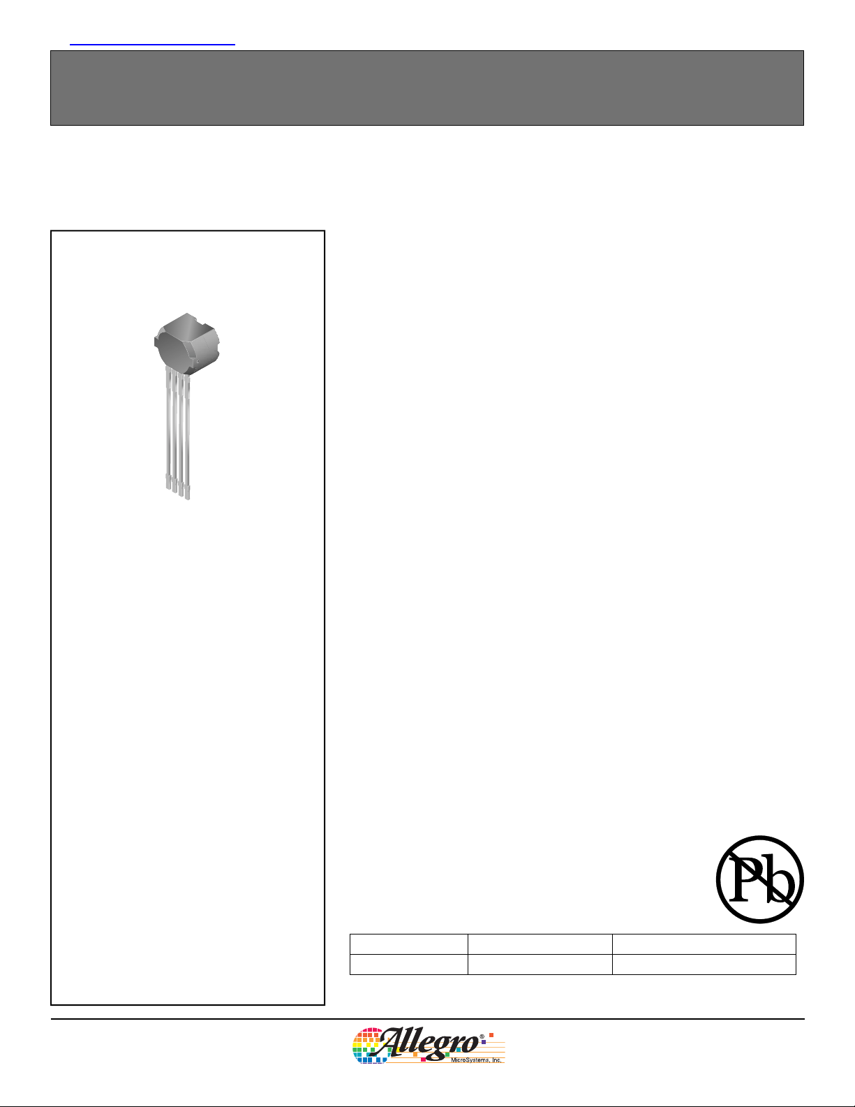
Package SG, 4-pin SIP
1
2
3
4
1. VCC
2. VOUT
3. Test Pin (Tie to GND)
4. GND
ATS616LSG
Hall Effect Gear Tooth Sensor
The ATS616 gear-tooth sensor is a peak-detecting device that uses automatic gain
control and an integrated capacitor to provide extremely accurate gear edge detection down to low operating speeds. Each sensor module consists of a high-temperature plastic shell that holds together a samarium-cobalt magnet, a pole piece,
and a differential open-collector Hall IC that has been optimized to the magnetic
circuit. This small package can be easily assembled and used in conjunction with a
wide variety of gear shapes and sizes.
The gear-sensing technology used for this sensor module is Hall-effect based. The
sensor incorporates a dual-element Hall IC that switches in response to differential
magnetic signals created by ferrous targets. The sophisticated processing circuitry
contains an A-to-D converter that self-calibrates (normalizes) the internal gain
of the device to minimize the effect of air-gap variations. The patented peakdetecting filter circuit eliminates magnet and system offsets and has the ability to
discriminate relatively fast changes such as those caused by tilt, gear wobble, and
eccentricities. This easy-to-integrate solution provides first-tooth detection and
stable operation to extremely low rpm. The ATS616 can be used as a replacement
for the ATS612LSB, eliminating the external peak-holding capacitor needed by
the ATS612LSB.
The ATS616 is ideal for use in systems that gather speed, position, and timing
information using gear-tooth-based configurations. This device is particularly
suited to those applications that require extremely accurate duty cycle control or
accurate edge-detection, such as automotive camshaft sensing.
AB SO LUTE MAX I MUM RAT INGS
Supply Voltage, V
Reverse-Supply Voltage, V
Output Off Voltage, V
Continuous Output Current, I
Reverse-Output Current, I
Operating Temperature
Ambient, T
Maximum Junction, T
Storage Temperature, T
*See Power Derating section.
ATS616LSG-DS, Rev. 1
.....................................26.5 V*
CC
OUTOFF
, Range L................ –40ºC to 150ºC
A
........................–18 V
RCC
............................ 24 V
...................25 mA
OUT
.......................50 mA
ROUT
........................165ºC
J(max)
.................. –65ºC to 170ºC
S
TheATS616 is provided in a 4-pin SIP that is Pb (lead) free, with a 100% matte
tin plated leadframe.
Features and Benefits
• Self-calibrating for tight timing accuracy
• First-tooth detection
• Immunity to air gap variation and system offsets
• Eliminates effects of signature tooth offsets
• Integrated capacitor provides analog peak and valley information
• Extremely low timing-accuracy drift with temperature changes
• Large air gap capability
• Small, integrated package
• Optimized magnetic circuit
• Undervoltage lockout (UVLO)
• Wide operating voltage range
Use the following complete part numbers when ordering:
Part Number Package Packing*
ATS616LSGTN-T 4-pin plastic SIP 13-in. reel, 800 pieces/reel
*Contact Allegro for additional packaging and handling options.
Allegro MicroSystems, Inc.
115 Northeast Cutoff, Box 15036
Worcester, Massachusetts 01615-0036 (508) 853-5000
www.allegromicro.com
ATS616LSG
Dynamic Self-Calibrating Peak-Detecting Differential Hall Effect Gear Tooth Sensor
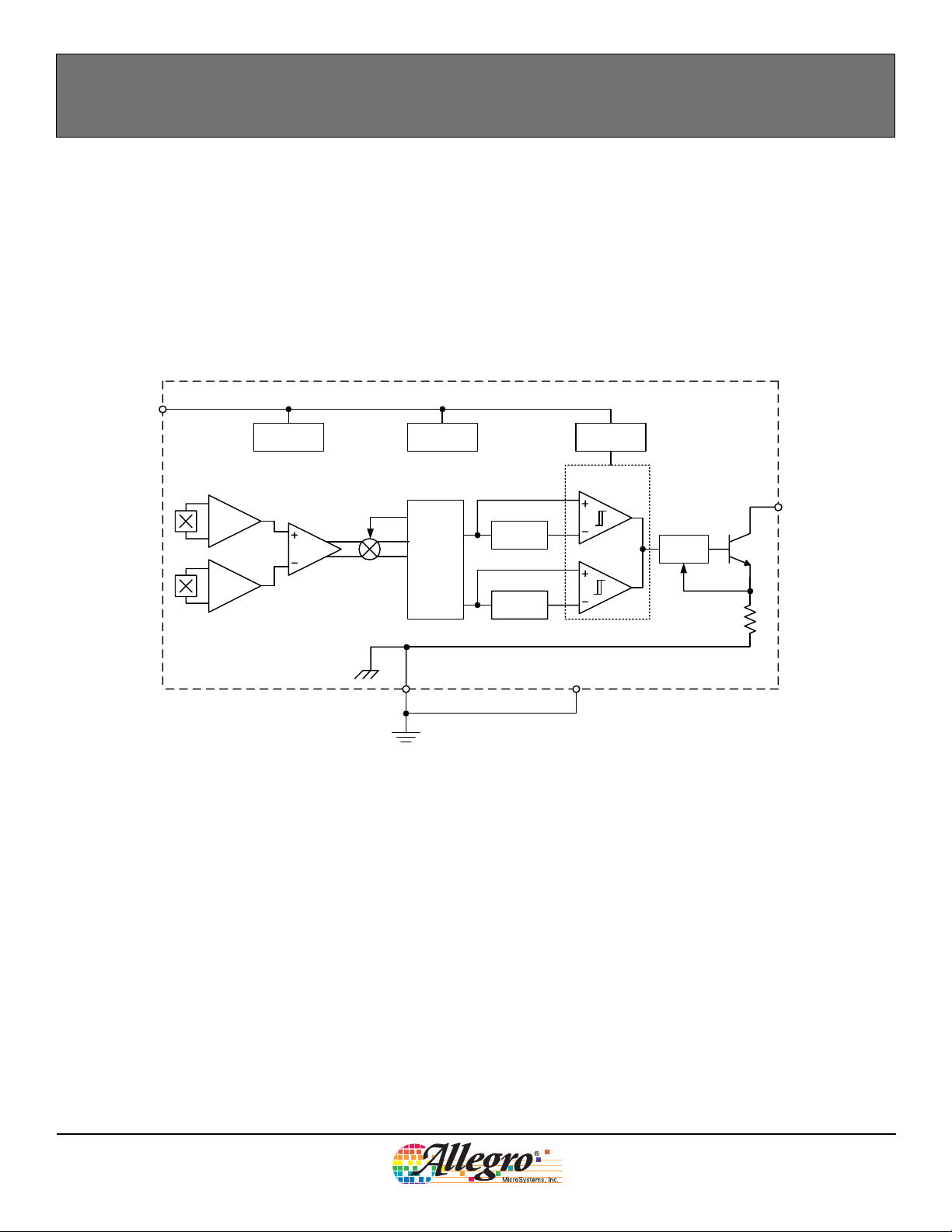
Functional Block Diagram
VCC
Hall
Amp
Hall
Amp
Voltage
Regulator
Gain
UVLO
Reference
Generator
GND
Track and
Hold
Track and
Hold
(Recommended)
Power-On
Logic
Tooth and Valley
Comparator
TEST
Current
Limit
VOUT
ATS616LSG-DS, Rev. 1
Allegro MicroSystems, Inc.
115 Northeast Cutoff, Box 15036
Worcester, Massachusetts 01615-0036 (508) 853-5000
www.allegromicro.com
2

ATS616LSG
Dynamic Self-Calibrating Peak-Detecting Differential Hall Effect Gear Tooth Sensor
OPERATING CHARACTERISTICS over operating voltage and temperature range, unless otherwise noted
Characteristic Symbol Test Condition Min. Typ.1Max. Units
ELECTRICAL CHARACTERISTICS
Supply Voltage
2
Power-On State POS VCC = 0 → 5 V – HIGH – V
V
Operating, TJ < 165°C 3.5 – 24 V
CC
Undervoltage Lockout Threshold V
Output On Voltage V
OUT(SAT)IOUT
Supply Zener Clamp Voltage V
Output Zener Clamp Voltage V
Supply Zener Current I
Output Zener Current I
Output Current Limit I
Output Leakage Current I
OUTOFFVOUT
Supply Current I
Power-On Time t
Output Rise Time
Output Fall Time
3
3
CC(UV)VCC
ZsupplyICC
ZoutputIOUT
ZsupplyVS
ZoutputVOUT
OUTMVOUT
CC
PO
t
r
t
f
= 0 → 5 V; VCC = 5 → 0 V – – 3.5 V
= 20 mA – 200 400 mV
= 16 mA, TA = 25°C 28 – – V
= 3 mA, TA = 25°C 30 – – V
= 28 V – – 15 mA
= 30 V – – 3 mA
= 12 V 25 45 55 mA
= 24 V – – 15 μA
VCC > V
CC(min)
3 6 12 mA
VCC > 5 V – 80 500 μs
R
= 500 Ω, CS = 10 pF – 0.3 5.0 μs
LOAD
R
= 500 Ω, CS = 10 pF – 0.2 5.0 μs
LOAD
PERFRORMANCE CHARACTERISTICS
Operating Air Gap Range AG Operating within specification, Target Speed > 10 rpm 0.4 – 2.5 mm
Operating Magnetic Flux Density
Differential
4
B
AG(p-p)
Operating within specification, Target Speed > 10 rpm 60 – – G
Operating Frequency ƒ 10 – 10 000 Hz
Initial Calibration Cycle
Calibration Mode Disable n
Relative Timing Accuracy, Sequential E
Allowable User Induced Differential Offset
1
Typical data is at VCC = 8 V and TA = 25°C. Performance may vary for individual units, within the specified maximum and minimum limits.
2
Maximum voltage must be adjusted for power dissipation and junction temperature; see Power Derating section.
3
CS is the probe capacitance of the oscilloscope used to make the measurement.
4
10 G = 1 mT (millitesla), exactly.
5
Non-uniform magnetic profiles may require additional edges before calibration is complete.
5
n
Output edges before calibration is completed, at f
cal
Output falling edges for startup calibration to be complete 64 64 64 Edge
dis
Target Speed = 1000 rpm, B
θ
Target Speed = 1000 rpm, B
4
ΔB
Output switching only; may not meet data sheet specifica-
App
tions
> 100 G – ±0.5 ±0.75
AG(p-p)
> 60 G – – ±1.5
AG(p-p)
< 100 Hz 1 1 1 Edge
sig
– – ±50 G
(°)
(°)
ATS616LSG-DS, Rev. 1
Allegro MicroSystems, Inc.
115 Northeast Cutoff, Box 15036
Worcester, Massachusetts 01615-0036 (508) 853-5000
www.allegromicro.com
3
ATS616LSG
Dynamic Self-Calibrating Peak-Detecting Differential Hall Effect Gear Tooth Sensor
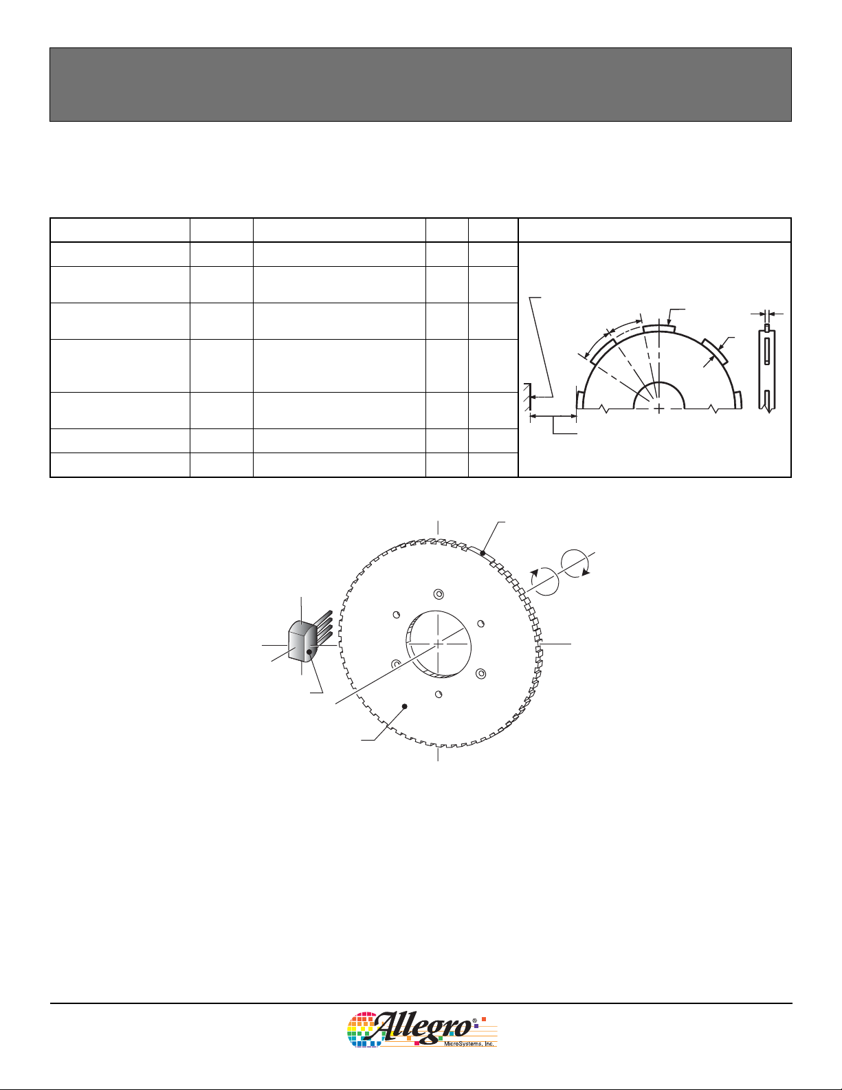
Reference Target (Gear) Information
REFERENCE TARGET 60+2
Characteristics Symbol Test Conditions Typ. Units Symbol Key
Outside Diameter D
Face Width F
Circular Tooth Length t
Signature Region Circular Tooth Length
Circular Valley Length t
Tooth Whole Depth h
Material Low Carbon Steel – –
t
SIG
Outside diameter of target
o
Breadth of tooth, with respect
to sensor
Length of tooth, with respect
to sensor; measured at D
Length of signature tooth,
with respect to sensor; measured at D
Length of valley, with respect
v
to sensor; measured at D
t
o
Pin 4
120 mm
6mm
3mm
o
15 mm
3mm
o
3mm
Branded Face
of Sensor
t,t
Air Gap
Signature Region
SIG
Ø
D
O
V
t
F
h
t
Pin 1
Branded Face
of Sensor
Reference Target
60+2
Figure 1. Configuration with Radial-Tooth Reference Target
For the generation of adequate magnetic field levels, the following recommendations should be followed in the design and
specification of targets:
• 2 mm < tooth width, t < 4 mm
• Valley width, tv > 2 mm
• Valley depth, ht > 2 mm
• Tooth thickness, F ≥ 3 mm
• Target material must be low carbon steel
ATS616LSG-DS, Rev. 1
Although these parameters apply to targets of traditional
geometry (radially oriented teeth with radial sensing, shown in
figure 1), they also can be applied in applications using stamped
targets (an aperture or rim gap punched out of the target mate-
rial) and axial sensing. For stamped geometries with axial sens-
ing, the valley depth, ht, is intrinsically infinite, so the criteria for
tooth width, t, valley width, tv, tooth material thickness, F, and
material specification need only be considered for reference. For
example, F can now be < 3 mm.
Allegro MicroSystems, Inc.
115 Northeast Cutoff, Box 15036
Worcester, Massachusetts 01615-0036 (508) 853-5000
www.allegromicro.com
4
ATS616LSG
Dynamic Self-Calibrating Peak-Detecting Differential Hall Effect Gear Tooth Sensor
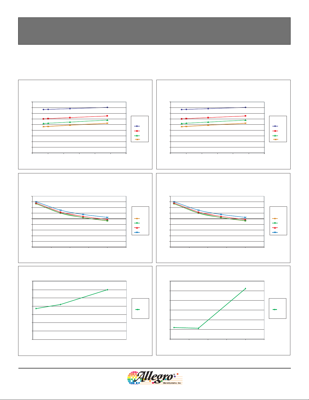
Characteristic Data
Supply Current (Off) versus Supply Voltage
9
8
7
6
(mA)
5
4
CCOFF
I
3
2
1
0
010201552530
VCC (V)
TA (°C)
–40
150
25
85
Supply Current (Off) versus Ambient Temperature
9
8
7
6
(mA)
5
4
CCOFF
I
3
2
1
0
–50 0 50 100 150 200
TA (°C)
VCC (V)
3.5
5.0
12
24
Supply Current (On) versus Supply Voltage
9
8
7
6
5
(mA)
4
CCON
I
3
2
1
0
010201552530
Supply Current (On) versus Ambient Temperature
9
8
7
6
(mA)
5
4
CCON
I
3
2
1
0
–50 0 50 100 150 200
V
(V)
VCC (V)
CC
TA (°C)
T
(°C)
A
–40
150
VCC (V)
3.5
12
24
25
85
5.0
Output Voltage (On) versus Ambient Temperature
350
300
250
(mV)
200
150
OUT(SAT)
V
100
50
0
–50 0 50 100 150 200
(°C)
T
A
Continued on the next page.
ATS616LSG-DS, Rev. 1
I
SINK
(mA)
20
Output Leakage Current versus Ambient Temperature
1.2
1.0
0.8
(µA)
0.6
OUTOFF
0.4
I
0.2
0
–50 0 50 100 150 200
TA (°C)
Allegro MicroSystems, Inc.
115 Northeast Cutoff, Box 15036
Worcester, Massachusetts 01615-0036 (508) 853-5000
www.allegromicro.com
V
(V)
OUT
10
5

ATS616LSG
Dynamic Self-Calibrating Peak-Detecting Differential Hall Effect Gear Tooth Sensor
Characteristic Data (continued)
Relative Timing Accuracy versus Air Gap
Sequential Tooth Falling Edge
1.5
1.0
0.5
0.0
-0.5
Edge Position (°)
-1.0
-1.5
0
1000 rpm
AG (mm)
Relative Timing Accuracy versus Air Gap
Signature Tooth Falling Edge
1000 rpm
-0.5
Edge Position (°)
-1.0
1.5
1.0
0.5
0.0
Relative Timing Accuracy versus Air Gap
Sequential
1.5
1.0
TA (°C)
–40
0
25
85
125
150
3.02.52.01.51.00.5
0.5
0.0
-0.5
Edge Position (°)
-1.0
-1.5
0
Tooth Rising Edge
1000 rpm
TA (°C)
–40
0
25
85
125
150
3.02.52.01.51.00.5
AG (mm)
TA (°C)
–40
125
150
Relative Timing Accuracy versus Air Gap
1.5
1.0
0.5
0
25
85
0.0
-0.5
Edge Position (°)
-1.0
Signature Tooth Rising Edge
1000 rpm
TA (°C)
–40
0
25
85
125
150
-1.5
0
ATS616LSG-DS, Rev. 1
AG (mm)
-1.5
3.02.52.01.51.00.5
0
3.02.52.01.51.00.5
AG (mm)
Allegro MicroSystems, Inc.
115 Northeast Cutoff, Box 15036
Worcester, Massachusetts 01615-0036 (508) 853-5000
www.allegromicro.com
6

ATS616LSG
Dynamic Self-Calibrating Peak-Detecting Differential Hall Effect Gear Tooth Sensor
Characteristic Data (continued)
Relative Timing Accuracy versus Ambient Temperature
Sequential Tooth Falling Edge
1.5
1.0
0.5
0.0
-0.5
Edge Position (°)
-1.0
-1.5
–50
0.5 mm
200150100500
TA (°C)
Relative Timing Accuracy versus Ambient Temperature
Sequential Tooth Rising Edge
0.5 mm
-0.5
Edge Position (°)
-1.0
1.5
1.0
0.5
0.0
Relative Timing Accuracy versus Ambient Temperature
rpm
100
500
1000
1500
2000
Signature
1.5
1.0
10
0.5
0.0
-0.5
Edge Position (°)
-1.0
-1.5
–50
Tooth Falling Edge
0.5 mm
rpm
200150100500
TA (°C)
Relative Timing Accuracy versus Ambient Temperature
1.5
rpm rpm
10
100
500
1000
1500
2000
1.0
0.5
0.0
-0.5
Edge Position (°)
-1.0
Signature Tooth Rising Edge
0.5 mm
10
100
500
1000
1500
2000
10
100
500
1000
1500
2000
-1.5
–50
ATS616LSG-DS, Rev. 1
-1.5
T
(°C)
A
200150100500
–50
TA (°C)
200150100500
Allegro MicroSystems, Inc.
115 Northeast Cutoff, Box 15036
Worcester, Massachusetts 01615-0036 (508) 853-5000
www.allegromicro.com
7

ATS616LSG
Dynamic Self-Calibrating Peak-Detecting Differential Hall Effect Gear Tooth Sensor
THERMAL CHARACTERISTICS may require derating at maximum conditions, see application information
Characteristic Symbol Test Conditions* Value Units
Single-sided PCB with copper limited to solder pads 126 ºC/W
Package Thermal Resistance
*Additional information is available on the Allegro Web site.
R
θJA
Two-sided PCB with copper limited to solder pads and 3.57 in.
(23.03 cm2) of copper area each side, connected to GND pin
Power Derating Curve
T
= 165ºC; ICC=I
25
24
23
22
21
(V)
20
CC
19
18
17
16
15
14
13
12
11
10
9
Maximum Allowable V
8
7
6
5
4
3
2
20 40 60 80 100 120 140 160 180
J(max)
(R
(R
= 84 ºC/W)
θJA
= 126 ºC/W)
θJA
Temperature (ºC)
CC(max)
V
CC(max)
V
CC(min)
2
84 ºC/W
ATS616LSG-DS, Rev. 1
Maximum Power Dissipation, P
1900
J(max)
CC(max);ICC=ICC(max)
T
= 165ºC; VCC=V
1800
1700
1600
1500
1400
1300
1200
(mW)
D
1100
1000
900
800
700
(
R
θJ
A
=
126 ºC/
=84
ºC/W)
W)
(R
θJA
600
500
400
Power Diss ipation, P
300
200
100
0
20 40 60 80 100 120 140 160 180
Temperature (°C)
D(max)
Allegro MicroSystems, Inc.
115 Northeast Cutoff, Box 15036
Worcester, Massachusetts 01615-0036 (508) 853-5000
www.allegromicro.com
8

ATS616LSG
Dynamic Self-Calibrating Peak-Detecting Differential Hall Effect Gear Tooth Sensor
Functional Description
Assembly Description. The ATS616 gear-tooth sensor is a
Hall IC/magnet configuration that is fully optimized to provide
digital detection of gear tooth edges. This sensor is packaged in
a molded miniature plastic body that has been optimized for size,
ease of assembly, and manufacturability. High operating temperature materials are used in all aspects of construction.
After proper power is applied to the component, the sensor is
capable of instantly providing digital information that is representative of the profile of a rotating gear. No additional optimization or processing circuitry is required. This ease of use should
reduce design time and incremental assembly costs for most
applications.
Sensing Technology. The gear tooth sensor module contains a
single-chip differential Hall effect sensor IC, a samarium cobalt
magnet, and a flat ferrous pole piece (figure 2). The Hall IC
consists of 2 Hall elements (spaced 2.2 mm apart) located so
as to measure the magnetic gradient created by the passing of a
ferrous object. The two elements measure the magnetic gradient
and convert it to an analog voltage that is then processed in order
to provide a digital output signal.
The Hall IC is self-calibrating and also possesses a temperature compensated amplifier and offset cancellation circuitry. Its
voltage regulator provides supply noise rejection throughout the
operating voltage range. Changes in temperature do not greatly
affect this device due to the stable amplifier design and the offset
rejection circuitry. The Hall transducers and signal processing
electronics are integrated on the same silicon substrate, using a
proprietary BiCMOS process.
Internal Electronics. The processing circuit uses a patented
peak detection scheme to eliminate magnet and system offsets.
This technique allows dynamic coupling and filtering of offsets
without the power-up and settling time disadvantages of classical
high-pass filtering schemes. The peak signal of every tooth and
valley is detected by the filter and is used to provide an instant
reference for the operate and release point comparator. In this
manner, the thresholds are adapted and referenced to individual
signal peaks and valleys, providing immunity to zero line variation from installation inaccuracies (tilt, rotation, and off-center
placement), as well as for variations caused by target and shaft
eccentricities. The peak detection concept also allows extremely
low speed operation for small value filter capacitors.
The ATS616 also includes self-calibration circuitry that is
engaged at power on. The signal amplitude is measured, and
then the device gain is normalized. In this manner switchpoint
drift versus air gap is minimized, and excellent timing accuracy
can be achieved.
The AGC (Automatic Gain Control) circuitry, in conjunction
with a unique hysteresis circuit, also eliminates the effect of
gear edge overshoot as well as increases the immunity to false
switching caused by gear tooth anomalies at close air gaps. The
Target (Gear)
Element Pitch
Hall Element 2
Dual-Element
Hall Effect Device
Figure 2. Relative motion of the target is detected by the dual Hall elements mounted on the Hall IC.
ATS616LSG-DS, Rev. 1
South Pole
North Pole
Hall Element 1
Hall IC
Pole Piece
(Concentrator)
Back-biasing Magnet
Case
(Pin 1 Side)(Pin n >1 Side)
B+
B
Differential
Magnetic Flux
0
B–
V
CC
Device Output
V
OUT
V
OUT(sat)
Figure 3. The peaks in the resulting differential signal are used to set the
operate, B
, and release, B
OP
OP
B
OP
B
B
RP
, switchpoints.
RP
Allegro MicroSystems, Inc.
115 Northeast Cutoff, Box 15036
Worcester, Massachusetts 01615-0036 (508) 853-5000
www.allegromicro.com
RP
9

ATS616LSG
Dynamic Self-Calibrating Peak-Detecting Differential Hall Effect Gear Tooth Sensor
AGC circuit sets the gain of the device after power-on. Up to a
0.25 mm air gap change can occur after calibration is complete
without significant performance impact.
Superior Performance. The ATS616 peak-detecting differential
gear-tooth sensor module has several advantages over conventional Hall-effect gear-tooth sensors. The signal-processing
techniques used in the ATS616 solve the catastrophic issues that
affect the functionality of conventional digital gear-tooth sensors, such as the following:
• Temperature drift. Changes in temperature do not greatly
affect this device due to the stable amplifier design and the
offset rejection circuitry.
• Timing accuracy variation due to air gap. The accuracy varia-
tion caused by air gap changes is minimized by the self-calibration circuitry. A 2×-to-3× improvement can be seen.
• Dual edge detection. Because this device switches based on
the positive and negative peaks of the signal, dual edge detection is guaranteed.
• Tilted or off-center installation. Traditional differential sensors
can switch incorrectly due to baseline changes versus air gap
caused by tilted or off-center installation. The peak detector circuitry references the switchpoint from the peak and is
immune to this failure mode. There may be a timing accuracy
shift caused by this condition.
classical single-element gear-tooth sensor. The single-element
configuration commonly used (Hall-effect sensor mounted on
the face of a simple permanent magnet) requires the detection
of a small signal (often <100 G) that is superimposed on a large
back-biased field, often 1500 G to 3500 G. For most gear/target
configurations, the back-biased field values change due to
concentration effects, resulting in a varying baseline with air
gap, valley widths, eccentricities, and vibration (figure 4). The
differential configuration (figure 5) cancels the effects of the
back-biased field and avoids many of the issues presented by the
single Hall element design.
• Large operating air gaps. Large operating air gaps are achiev-
able with this device due to the sensitive switchpoints after
power-on (dependent on target dimensions, material, and
speed).
• Immunity to magnetic overshoot. The patented adjustable
hysteresis circuit makes the ATS616 immune to switching on
magnetic overshoot within the specified air gap range.
• Response to surface defects in the target. The gain-adjust
circuitry reduces the effect of minor gear anomalies that would
normally cause false switching.
• Immunity to vibration and backlash. The gain-adjust circuitry
keeps the hysteresis of the device roughly proportional to the
peak-to-peak signal. This allows the device to have good immunity to vibration even when operating at close air gaps.
• Immunity to gear run out. The differential sensor configura-
tion eliminates the baseline variations caused by gear run out.
Differential vs. Single-Element Sensing. The differential
Hall-effect configuration is superior in most applications to the
ATS616LSG-DS, Rev. 1
Figure 4. Affect of varying valley widths on single-element sensors.
Figure 4. Affect of varying air gaps on differential sensors.
Allegro MicroSystems, Inc.
115 Northeast Cutoff, Box 15036
Worcester, Massachusetts 01615-0036 (508) 853-5000
www.allegromicro.com
10

ATS616LSG
of Sensor
Rotating Target
Branded Face
1
4
Dynamic Self-Calibrating Peak-Detecting Differential Hall Effect Gear Tooth Sensor
Peak Detecting vs. AC-Coupled Filters. High-pass filtering
(normal ac coupling) is a commonly used technique for eliminating circuit offsets. However, ac coupling has errors at power-on
because the filter circuit needs to hold the circuit zero value
even though the circuit may power-on over a large signal. Such
filtering techniques can only perform properly after the filter
has been allowed to settle, which typically takes longer than 1s.
Also, high-pass filter solutions cannot easily track rapidly changing baselines, such as those caused by eccentricities. (The term
baseline refers to a 0 G differential field, where each Hall-effect
element is subject to the same magnetic field strength; see figure
3.) In contrast, peak detecting designs switch at the change in
slope of the differential signal, and so are baseline-independent
both at power-on and while running.
Peak Detecting vs. Zero-Crossing Reference. The usual dif-
ferential zero-crossing sensors are susceptible to false switching
due to off-center and tilted installations that result in a shift of
the baseline that changes with air gap. The track-and-hold peak
detection technique ignores baseline shifts versus air gaps and
provides increased immunity to false switching. In addition,
using track-and-hold peak detection techniques, increased air
gap capabilities can be expected because peak detection utilizes
the entire peak-to-peak signal range, as compared to zero-crossing detectors, which switch at half the peak-to-peak signal.
is below the minimum operating voltage, V
CC(UV)
, the device is
off and stays off, irrespective of the state of the magnetic field.
This prevents false signals, which may be caused by undervoltage conditions (especially during power-up), from appearing at
the output.
Output. The device output is an open-collector stage capable of
sinking up to 20 mA. An external pull-up (resistor) must be supplied to a supply voltage of not more than 24 V.
Output Polarity. The output of the unit will switch from low to
high as the leading edge of a tooth passes the branded face of the
sensor in the direction indicated in figure 6. This means that in
such a configuration, the output voltage will be high when the
sensor is facing a tooth. If the target rotation is in the opposite direction relative to the sensor, the output polarity will be
opposite as well, with the unit switching from low to high as the
leading edge passes the unit.
Power-On Operation. The device powers-on in the Off state
(output voltage high), irrespective of the magnetic field condition. The power-up time of the circuit is no greater than 500 μs.
The circuit is then ready to accurately detect the first target edge
that results in a high-to-low transition of the device output.
Undervoltage Lockout (UVLO). When the supply voltage, V
Target
Mechanical Profile
Target
Magnetic Profile
Sensor Output
Switch State
Sensor Output
Electrical Profile
Target Motion from
Pin 1 to Pin 4
Sensor Output
Electrical Profile
Target Motion from
Pin 4 to Pin 1
B+
B
IN
On Off On Off On Off On Off On OffOn OffOn OffOn Off
V+
V
OUT
V+
V
OUT
CC
Figure 6. This left-to-right (pin 1 to pin 4) direction of target rotation
results in a high output signal when a tooth of the target gear is nearest
the branded face of the sensor. A right-to-left (pin 4 to pin 1) rotation
inverts the output signal polarity.
,
Signature Tooth
Figure 7. The magnetic profile reflects the geometry of the target, allowing the device to present an accurate digital output response.
ATS616LSG-DS, Rev. 1
Allegro MicroSystems, Inc.
115 Northeast Cutoff, Box 15036
Worcester, Massachusetts 01615-0036 (508) 853-5000
www.allegromicro.com
11

ATS616LSG
Dynamic Self-Calibrating Peak-Detecting Differential Hall Effect Gear Tooth Sensor
Power Derating
The device must be operated below the maximum junction
temperature of the device, T
. Under certain combinations of
J(max)
peak conditions, reliable operation may require derating supplied power or improving the heat dissipation properties of the
application. This section presents a procedure for correlating
factors affecting operating TJ. (Thermal data is also available on
the Allegro MicroSystems Web site.)
The Package Thermal Resistance, R
, is a figure of merit sum-
θJA
marizing the ability of the application and the device to dissipate
heat from the junction (die), through all paths to the ambient air.
Its primary component is the Effective Thermal Conductivity,
K, of the printed circuit board, including adjacent devices and
traces. Radiation from the die through the device case, R
relatively small component of R
. Ambient air temperature,
θJA
θJC
, is
TA, and air motion are significant external factors, damped by
overmolding.
The effect of varying power levels (Power Dissipation, PD), can
be estimated. The following formulas represent the fundamental
relationships used to estimate TJ, at PD.
PD = VIN × I
ΔT = PD × R
IN
(2)
θJA
(1)
TJ = TA + ΔT (3)
For example, given common conditions such as: TA= 25°C,
V
= 12 V, I
CC
PD = VCC × I
ΔT = PD × R
= 4 mA, and R
CC
= 12 V × 4 mA = 48 mW
CC
= 48 mW × 140°C/W = 7°C
θJA
θJA
= 140°C/W, then:
A worst-case estimate, P
able power level (V
at a selected R
and TA.
θJA
CC(max)
Example: Reliability for V
, represents the maximum allow-
D(max)
, I
CC
), without exceeding T
CC(max)
at TA = 150°C, package SG, using
J(max)
,
minimum-K PCB.
Observe the worst-case ratings for the device, specifically:
R
126°C/W, T
θJA =
I
CC(max) =
12 mA.
Calculate the maximum allowable power level, P
J(max) =
165°C, V
CC(max) = 24
V, and
D(max)
. First,
invert equation 3:
ΔT
max
= T
– TA = 165 °C – 150 °C = 15 °C
J(max)
This provides the allowable increase to TJ resulting from internal
power dissipation. Then, invert equation 2:
P
D(max)
= ΔT
max
÷ R
= 15°C ÷ 126°C/W = 119 mW
θJA
Finally, invert equation 1 with respect to voltage:
V
CC(est)
= P
D(max)
÷ I
= 119 mW ÷ 12 mA = 9.92 V
CC(max)
The result indicates that, at TA, the application and device can
dissipate adequate amounts of heat at voltages ≤V
Compare V
CC(est)
to V
able operation between V
R
θJA
V
CC(max)
. If V
is reliable under these conditions.
CC(est)
≥ V
CC(max)
CC(max)
CC(est)
. If V
and V
CC(est)
CC(max)
≤ V
, then operation between V
CC(max)
requires enhanced
.
CC(est)
, then reli-
CC(est)
and
This value applies only to the voltage drop across the ATS616
chip. If a protective series diode or resistor is used, the effective maximum supply voltage is increased. For example, when a
standard diode with a 0.7 V drop is used:
TJ = TA + ΔT = 25°C + 7°C = 32°C
ATS616LSG-DS, Rev. 1
V
CC(max)
= 9.9 V + 0.7 V = 10.6 V
Allegro MicroSystems, Inc.
115 Northeast Cutoff, Box 15036
Worcester, Massachusetts 01615-0036 (508) 853-5000
www.allegromicro.com
12

ATS616LSG
Dynamic Self-Calibrating Peak-Detecting Differential Hall Effect Gear Tooth Sensor
Sensor Evaluation: EMC (Electromagnetic Compatibility)
Characterization Only
Test Name* Reference Specification
ESD – Human Body Model AEC-Q100-002
ESD – Machine Model AEC-Q100-003
Conducted Transients ISO 7637-1
Direct RF Injection ISO 11452-7
Bulk Current Injection ISO 11452-4
TEM Cell ISO 11452-3
*Please contact Allegro MicroSystems for EMC performance
Mechanical Information
Component Material Description Value
Sensor Package Material Thermoset Epoxy Maximum Temperature 170°C
Leads Copper 0.016 in. thick
a
Temperature excursions of up to 225°C for 2 minutes or less are permitted.
b
Industry accepted soldering techniques are acceptable for this package as long as the indicated maximum temperature is not exceeded.
Additional soldering information is available on the Allegro Web site.
a
ATS616LSG-DS, Rev. 1
Allegro MicroSystems, Inc.
115 Northeast Cutoff, Box 15036
Worcester, Massachusetts 01615-0036 (508) 853-5000
www.allegromicro.com
13

ATS616LSG
Dynamic Self-Calibrating Peak-Detecting Differential Hall Effect Gear Tooth Sensor
Package SG Module
5.5 .217
.0866
2.2
NOM
8.0 .315
5.8 .228
2.9 .114
4.7 .185
20.95 .825
15.3 .602
Preliminary dimensions, for reference only
Untoleranced dimensions are nominal.
Dimensions in millimeters
U.S. Customary dimensions (in.) in brackets, for reference only
Dimensions exclusive of mold flash, burrs, and dambar protrusions
Exact case and lead configuration at supplier discretion within limits shown
E1
1.7 .067
0.6
.024
C
E2
A
2431
0.4 .016
A
1.27 .050
Dambar removal protrusion
A
Metallic protrusion, electrically connected to pin 4 and substrate (both sides)
B
Active Area Depth
C
Thermoplastic Molded Lead Bar for alignment during shipment
D
B
0.38 .015
1.08 .043
D
The products described herein are manufactured under one or more of the following U.S. patents: 5,045,920; 5,264,783; 5,442,283; 5,389,889;
5,581,179; 5,517,112; 5,619,137; 5,621,319; 5,650,719; 5,686,894; 5,694,038; 5,729,130; 5,917,320; and other patents pending.
Allegro MicroSystems, Inc. reserves the right to make, from time to time, such de par tures from the detail spec i fi ca tions as may be required to
permit improvements in the per for mance, reliability, or manufacturability of its products. Before placing an order, the user is cautioned to verify that
the information being relied upon is current.
Allegro products are not authorized for use as critical components in life-support devices or sys tems without express written approval.
The in for ma tion in clud ed herein is believed to be ac cu rate and reliable. How ev er, Allegro MicroSystems, Inc. assumes no re spon si bil i ty for its
use; nor for any in fringe ment of patents or other rights of third parties which may result from its use.
Copyright © 2005 Allegro MicroSystems, Inc.
ATS616LSG-DS, Rev. 1
Allegro MicroSystems, Inc.
115 Northeast Cutoff, Box 15036
Worcester, Massachusetts 01615-0036 (508) 853-5000
www.allegromicro.com
14
 Loading...