

ALLEGRO ACS754SCB-200 User Manual
Current Sensor: ACS754SCB-200
5
4
1
2
3
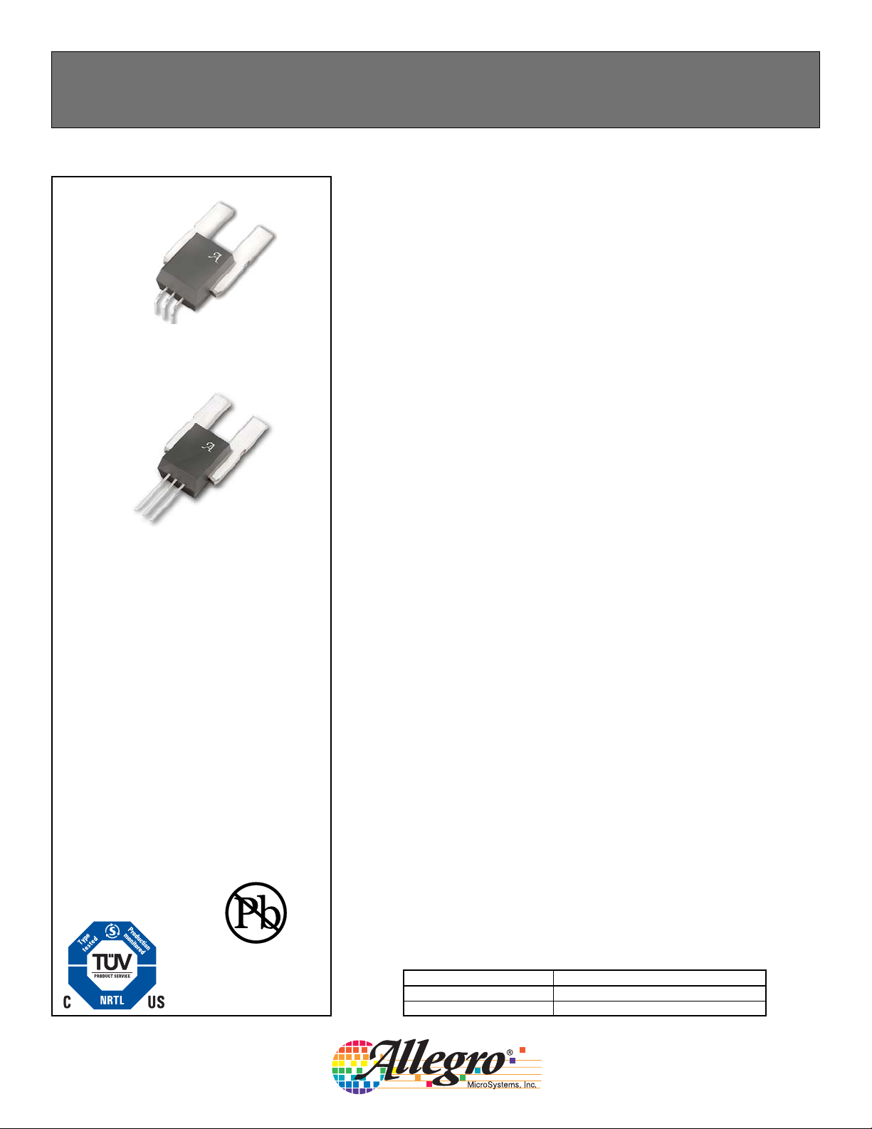
Package CB-PSF
5
4
1
2
3
Package CB-PSS
Pin 1: VCC
Pin 2: GND
Pin 3: VOUT
AB SO LUTE MAX I MUM RAT INGS
Supply Voltage, VCC..........................................16 V
Reverse Supply Voltage, V
Output Voltage, V
Reverse Output Voltage, V
Output Current Source, I
Output Current Sink, I
Operating Temperature,
Ambient, T
Maximum Junction, T
Maximum Storage Temperature, T
OUT
, S range ....................... –20 to 85ºC
A
Terminal 4: IP+
Terminal 5: IP–
........................–16 V
RCC
........................................16 V
...................... –0.1 V
ROUT
OUT(Source)
OUT(Sink)
.......................10 mA
....................... 165°C
J(max)
S
................. 3 mA
....–65 to 170°C
The Allegro ACS75x family of current sensors provides economical and
precise solutions for current sensing in industrial, automotive, commercial, and
communications systems. The device package allows for easy implementation
by the customer. Typical applications include motor control, load detection and
management, power supplies, and overcurrent fault protection.
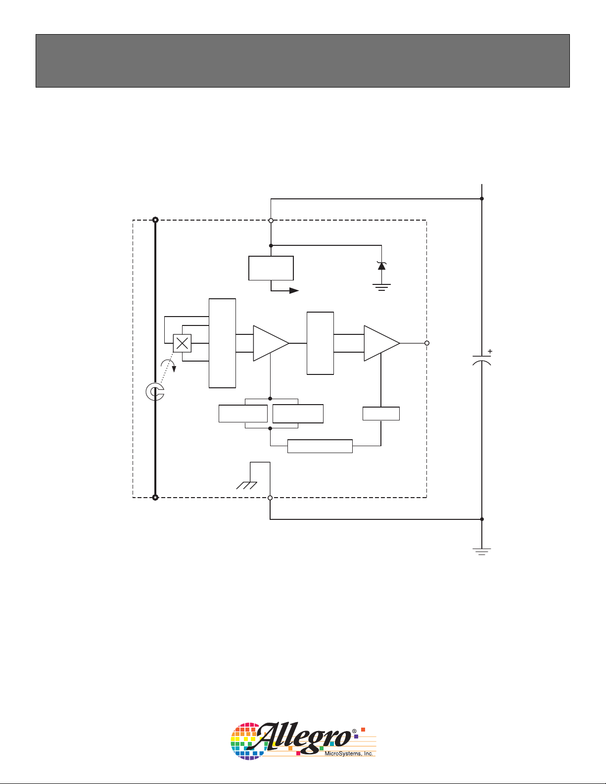
The device consists of a precision, low-offset linear Hall sensor circuit with a
copper conduction path located near the die. Applied current fl owing through
this copper conduction path generates a magnetic fi eld which is sensed by the
integrated Hall IC and converted into a proportional voltage. Device accuracy
is optimized through the close proximity of the magnetic signal to the Hall
transducer. A precise, proportional voltage is provided by the low-offset, chopperstabilized BiCMOS Hall IC, which is programmed for accuracy at the factory.
The output of the device has a positive slope (>V
/ 2) when an increasing
CC
current fl ows through the primary copper conduction path (from terminal 4 to
terminal 5), which is the path used for current sensing. The internal resistance of
this conductive path is typically 100 µΩ, providing low power loss. The thickness
of the copper conductor allows survival of the device at up to 5× overcurrent
conditions. The terminals of the conductive path are electrically isolated from the
sensor leads (pins 1 through 3). This allows the ACS75x family of sensors to be
used in applications requiring electrical isolation without the use of opto-isolators
or other costly isolation techniques.
The device is fully calibrated prior to shipment from the factory. The ACS75x
family is lead-free. All leads are coated with 100% matte tin, and there is no lead
inside the package. The heavy gauge leadframe is made of oxygen-free copper.
Features and Benefi ts
• Monolithic Hall IC for high reliability
• Single +5 V supply
• 3 kV
isolation voltage between terminals 4/5 and pins 1/2/3
RMS
• 35 kHz bandwidth
• End-of-line factory-trimmed for gain and offset
• Ultra-low power loss: 100 µΩ internal conductor resistance
• Ratiometric output from supply voltage
• Extremely stable output offset voltage
• Small package size, with easy mounting capability
• Output proportional to ac and dc currents
Applications
• Industrial systems
• Motor control
• Servo systems
• Power conversion
• Battery monitors
TÜV America
Certifi cate Number:
U8V 04 11 54214 001
ACS754200-DS, Rev. 3
Use the following complete part numbers when ordering:
Part Number Package
ACS754SCB-200-PSF Formed signal pins
ACS754SCB-200-PSS Straight signal pins
115 Northeast Cutoff, Box 15036
Worcester, Massachusetts 01615-0036 (508) 853-5000
Current Sensor: ACS754SCB-200
Functional Block Diagram
+5 V
IP–
Terminal 5
Cancellation
Dynamic Offset
Gain
VCC
Pin 1
Voltage
Regulator
To all subcircuits
Amp Out
Temperature
Coefficient
Filter
Trim Control
Offset
VOUT
Pin 3
0.1 µF
ACS754200-DS, Rev. 3
IP+
Terminal 4
GND
Pin 2
115 Northeast Cutoff, Box 15036
Worcester, Massachusetts 01615-0036 (508) 853-5000
2
Current Sensor: ACS754SCB-200
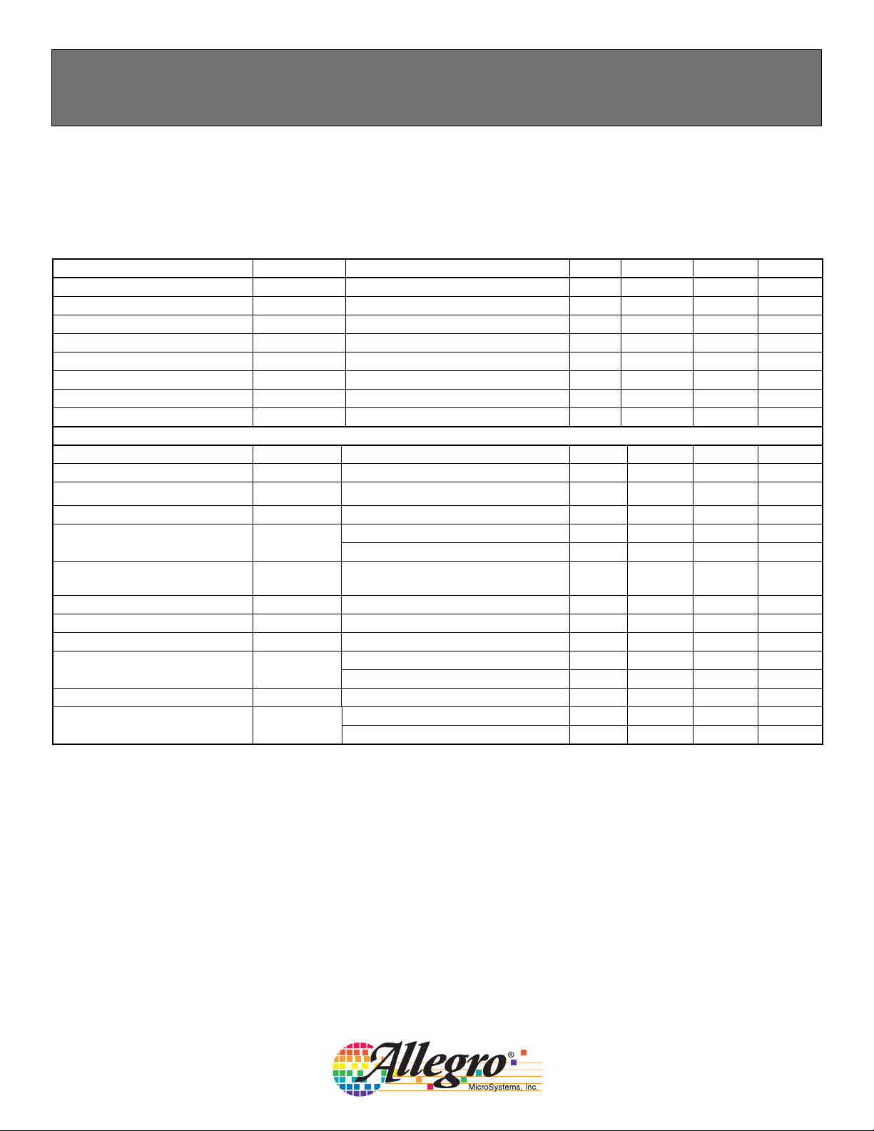
ELECTRICAL CHARACTERISTICS, over operating ambient temperature range unless otherwise stated
Characteristic Symbol Test Conditions Min. Typ. Max. Units
Primary Sensed Current I
Supply Voltage V
Supply Current I
Output Resistance R
Output Capacitance Load C
Output Resistive Load R
Primary Conductor Resistance R
Isolation Voltage V
P
CC
CC
OUT
LOAD
LOAD
PRIMARYIP
ISO
VCC = 5.0 V, output open 6.5 8 10 mA
I
= 1.2 mA – 1 2 Ω
OUT
VOUT to GND – – 10 nF
VOUT to GND 4.7 – – kΩ
= ±50A; TA = 25°C – 100 – µΩ
Pins 1-3 and 4-5; 60 Hz, 1 minute 3.0 – – kV
PERFORMANCE CHARACTERISTICS, -20°C to +85°C, VCC = 5 V unless otherwise specifi ed
Propagation time t
Response time t
PROP
RESPONSEIP
Rise time t
r
IP = ±100 A, TA = 25°C – 4 – µs
= ±100 A, TA = 25°C – 11 – µs
IP = ±100 A, T A= 25°C – 10 – µs
Frequency Bandwidth f –3 dB, T = 25°C – 35 – kHz
Sensitivity Sens
Noise V
Nonlinearity E
Symmetry E
Zero Current Output Voltage V
Electrical Offset Voltage
(Magnetic error not included)
Magnetic Offset Error
Total Output Error
(Including all offsets)
NOISE
LIN
SYM
OUT(Q)
V
OE
I
ERROM
E
TOT
Over full range of IP , TA = 25°C – 10.0 – mV/A
Over full range of I
P
Peak-to-peak, TA = 25°C,
no external fi lter
Over full range of I
Over full range of I
P
P
I = 0 A, TA= 25°C – VCC / 2 – V
I = 0 A, TA = 25°C –10 – 10 mV
I = 0 A –20 – 20 mV
I = 0 A, after excursion of 200 A – ±0.15 ±0.50 A
Over full range of IP , TA = 25°C – ±1.0 – %
Over full range of I
P
–200 – 200 A
4.5 5.0 5.5 V
9.5 – 10.5 mV/A
–35 –mV
– – ±0.8 %
98 100 102 %
– – ±5.0 %
ACS754200-DS, Rev. 3
115 Northeast Cutoff, Box 15036
Worcester, Massachusetts 01615-0036 (508) 853-5000
3
 Loading...