

Page 1

ACS712
Fully Integrated, Hall Effect-Based Linear Current Sensor IC
with 2.1 kVRMS Isolation and a Low-Resistance Current Conductor
Not for New Design
These parts are in production but have been determined to be
NOT FOR NEW DESIGN. This classification indicates that sale of
this device is currently restricted to existing customer applications.
The device should not be purchased for new design applications
because obsolescence in the near future is probable. Samples are no
longer available.
Date of status change: June 5, 2017
Recommended Substitutions:
For existing customer transition, and for new customers or new applications, use ACS723.
NOTE: For detailed information on purchasing options, contact your
local Allegro field applications engineer or sales representative.
Allegro MicroSystems, LLC reserves the right to make, from time to time, revisions to the anticipated product life cycle plan
for a product to accommodate changes in production capabilities, alternative product availabilities, or market demand. The
information included herein is believed to be accurate and reliable. However, Allegro MicroSystems, LLC assumes no responsibility for its use; nor for any infringements of patents or other rights of third parties which may result from its use.
Page 2
ACS712
Fully Integrated, Hall Effect-Based Linear Current Sensor IC
with 2.1 kVRMS Isolation and a Low-Resistance Current Conductor
Features and Benefits
▪ Low-noise analog signal path
▪ Device bandwidth is set via the new FILTER pin
▪ 5 µs output rise time in response to step input current
▪ 80 kHz bandwidth
▪ Total output error 1.5% at T
= 25°C
A
▪ Small footprint, low-profile SOIC8 package
▪ 1.2 mΩ internal conductor resistance
▪ 2.1 kVRMS minimum isolation voltage from pins 1-4 to pins 5-8
▪ 5.0 V, single supply operation
▪ 66 to 185 mV/A output sensitivity
▪ Output voltage proportional to AC or DC currents
▪ Factory-trimmed for accuracy
▪ Extremely stable output offset voltage
▪ Nearly zero magnetic hysteresis
▪ Ratiometric output from supply voltage
TÜV America
Certificate Number:
U8V 06 05 54214 010
Package: 8 Lead SOIC (suffix LC)
Description
The Allegro™ ACS712 provides economical and precise
solutions for AC or DC current sensing in industrial, commercial,
and communications systems. The device package allows for
easy implementation by the customer. Typical applications
include motor control, load detection and management, switchmode power supplies, and overcurrent fault protection. The
device is not intended for automotive applications.
The device consists of a precise, low-offset, linear Hall circuit
with a copper conduction path located near the surface of the
die. Applied current flowing through this copper conduction
path generates a magnetic field which the Hall IC converts into a
proportional voltage. Device accuracy is optimized through the
close proximity of the magnetic signal to the Hall transducer.
A precise, proportional voltage is provided by the low-offset,
chopper-stabilized BiCMOS Hall IC, which is programmed
for accuracy after packaging.
The output of the device has a positive slope (>V
when an increasing current flows through the primary copper
conduction path (from pins 1 and 2, to pins 3 and 4), which is
the path used for current sampling. The internal resistance of
this conductive path is 1.2 mΩ typical, providing low power
loss. The thickness of the copper conductor allows survival of
IOUT(Q)
)
Approximate Scale 1:1
Continued on the next page…
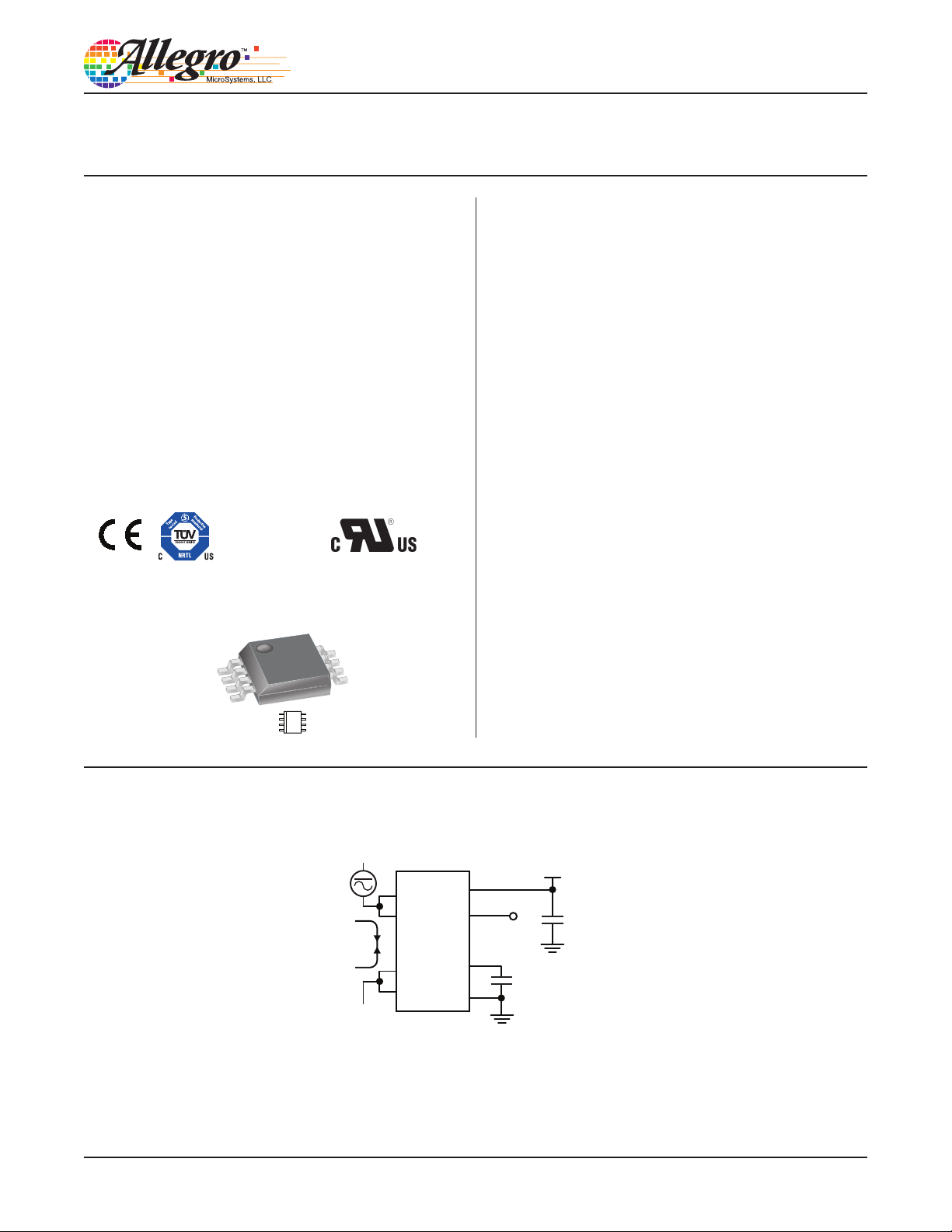
Typical Application
1
IP+
2
IP+
I
Application 1. The ACS712 outputs an analog signal, V
that varies linearly with the uni- or bi-directional AC or DC
primary sampled current, IP , within the range specified. CF
is recommended for noise management, with values that
depend on the application.
ACS712
P
3
FILTER
IP–
4
IP–
VCC
VIOUT
GND
8
7
6
5
V
C
1 nF
OUT
+5 V
C
BYP
0.1 µF
F
OUT
.
ACS712-DS, Rev. 16
June 5, 2017
Page 3

ACS712
Fully Integrated, Hall Effect-Based Linear Current Sensor IC
with
2.1 kVRMS Isolation and a Low-Resistance Current Conductor
Description (continued)
the device at up to 5× overcurrent conditions. The terminals of the
conductive path are electrically isolated from the signal leads (pins
5 through 8). This allows the ACS712 to be used in applications
requiring electrical isolation without the use of opto-isolators or
other costly isolation techniques.
The ACS712 is provided in a small, surface mount SOIC8 package.
The leadframe is plated with 100% matte tin, which is compatible
with standard lead (Pb) free printed circuit board assembly processes.
Internally, the device is Pb-free, except for flip-chip high-temperature
Pb-based solder balls, currently exempt from RoHS. The device is
fully calibrated prior to shipment from the factory.
Selection Guide
Part Number Packing*
ACS712ELCTR-05B-T Tape and reel, 3000 pieces/reel –40 to 85 ±5 185
ACS712ELCTR-20A-T Tape and reel, 3000 pieces/reel –40 to 85 ±20 100
ACS712ELCTR-30A-T Tape and reel, 3000 pieces/reel –40 to 85 ±30 66
*Contact Allegro for additional packing options.
TA
(°C)
Optimized Range, IP
(A)
Sensitivity, Sens
(Typ) (mV/A)
Absolute Maximum Ratings
Characteristic Symbol Notes Rating Units
Supply Voltage V
Reverse Supply Voltage V
Output Voltage V
Reverse Output Voltage V
Output Current Source I
Output Current Sink I
Overcurrent Transient Tolerance I
Nominal Operating Ambient Temperature T
Maximum Junction Temperature T
Storage Temperature T
IOUT(Source)
IOUT(Sink)
J
CC
RCC
IOUT
RIOUT
P
A
(max) 165 ºC
stg
1 pulse, 100 ms 100 A
Range E –40 to 85 ºC
8 V
–0.1 V
8 V
–0.1 V
3 mA
10 mA
–65 to 170 ºC
Isolation Characteristics
Characteristic Symbol Notes Rating Unit
Dielectric Strength Test Voltage* V
Working Voltage for Basic Isolation V
Working Voltage for Reinforced Isolation V
* Allegro does not conduct 60-second testing. It is done only during the UL certification process.
ISO
WFSI
WFRI
Agency type-tested for 60 seconds per
UL standard 60950-1, 1st Edition
For basic (single) isolation per UL standard
60950-1, 1st Edition
For reinforced (double) isolation per UL standard
60950-1, 1st Edition
Parameter Specification
CAN/CSA-C22.2 No. 60950-1-03
Fire and Electric Shock
UL 60950-1:2003
EN 60950-1:2001
2100 VAC
354 VDC or V
184 VDC or V
Allegro MicroSystems, LLC
115 Northeast Cutoff
Worcester, Massachusetts 01615-0036 U.S.A.
1.508.853.5000; www.allegromicro.com
pk
pk
2
Page 4
ACS712
+5 V
VCC
(Pin 8)
Hall Current
Drive
Fully Integrated, Hall Effect-Based Linear Current Sensor IC
with
2.1 kVRMS Isolation and a Low-Resistance Current Conductor
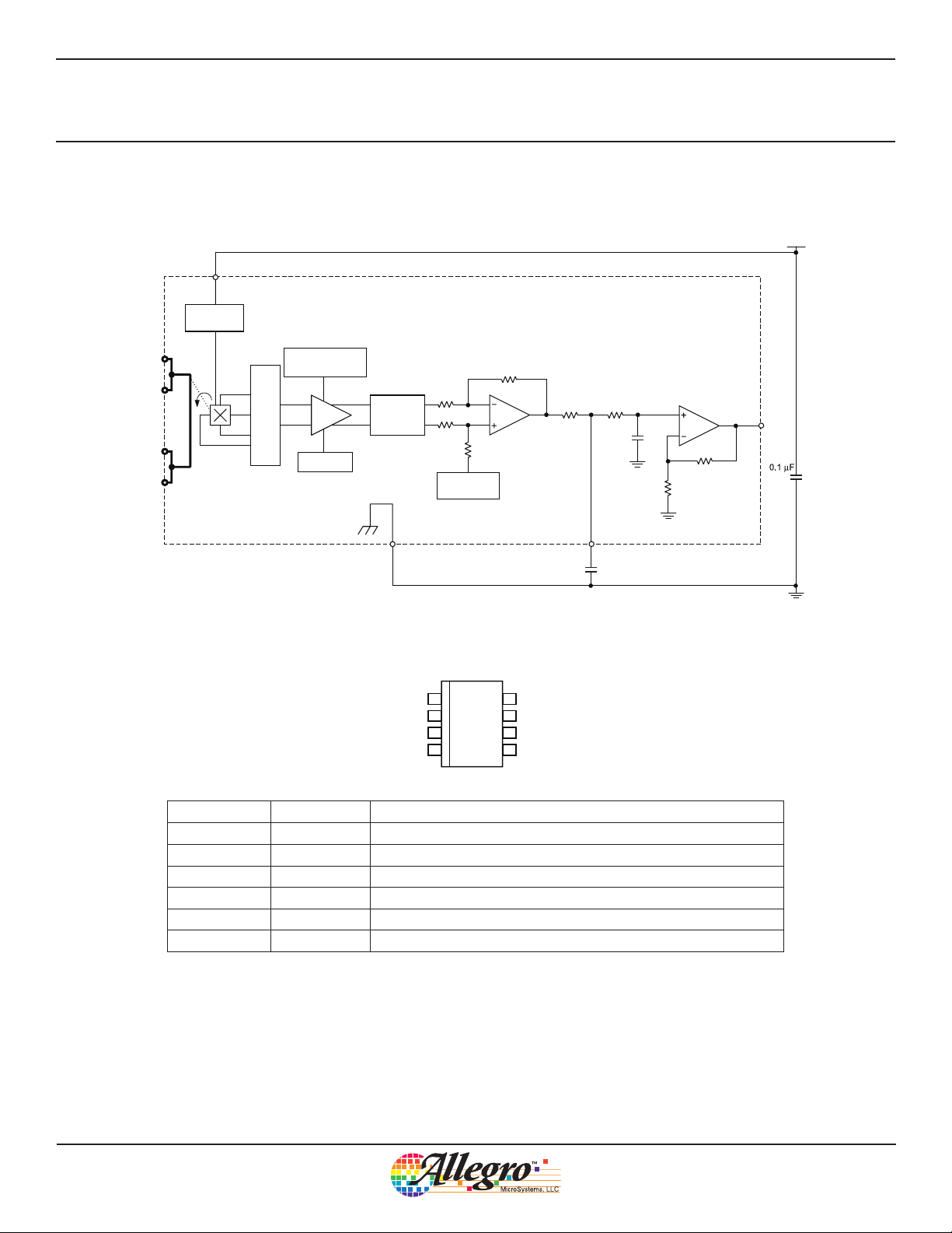
Functional Block Diagram
IP+
(Pin 1)
IP+
(Pin 2)
IP−
(Pin 3)
IP−
(Pin 4)
Terminal List Table
Number Name Description
1 and 2 IP+ Terminals for current being sampled; fused internally
3 and 4 IP– Terminals for current being sampled; fused internally
5 GND Signal ground terminal
6 FILTER Terminal for external capacitor that sets bandwidth
7 VIOUT Analog output signal
8 VCC Device power supply terminal
Sense Temperature
Coefficient Trim
Cancellation
Dynamic Offset
Sense
Trim
GND
(Pin 5)
Signal
Recovery
0 Ampere
Offset Adjust
Pin-out Diagram
1
IP+
2
IP+
3
IP–
4
IP–
8
7
6
5
VCC
VIOUT
FILTER
GND
R
F(INT)
FILTER
(Pin 6)
VIOUT
(Pin 7)
Allegro MicroSystems, LLC
115 Northeast Cutoff
Worcester, Massachusetts 01615-0036 U.S.A.
1.508.853.5000; www.allegromicro.com
3
Page 5
ACS712
Fully Integrated, Hall Effect-Based Linear Current Sensor IC
with
2.1 kVRMS Isolation and a Low-Resistance Current Conductor
COMMON OPERATING CHARACTERISTICS
1
over full range of TA , CF = 1 nF, and VCC = 5 V, unless otherwise specified
Characteristic Symbol Test Conditions Min. Typ. Max. Units
ELECTRICAL CHARACTERISTICS
Supply Voltage V
Supply Current I
Output Capacitance Load C
Output Resistive Load R
Primary Conductor Resistance R
Rise Time t
Frequency Bandwidth f –3 dB, T
Nonlinearity E
Symmetry E
Zero Current Output Voltage V
Power-On Time t
Magnetic Coupling
Internal Filter Resistance
1
Device may be operated at higher primary current levels, IP, and ambient, TA , and internal leadframe temperatures, TA , provided that the Maximum
2
3
CC
CC
LOAD
LOAD
PRIMARYTA
r
LIN
SYM
IOUT(Q)
PO
R
F(INT)
VCC = 5.0 V, output open – 10 13 mA
VIOUT to GND – – 10 nF
VIOUT to GND 4.7 – – kΩ
= 25°C – 1.2 – mΩ
IP = IP(max), TA = 25°C, C
= 25°C; IP is 10 A peak-to-peak – 80 – kHz
A
Over full range of I
Over full range of I
P
P
= open – 3.5 – μs
OUT
Bidirectional; IP = 0 A, TA = 25°C –
Output reaches 90% of steady-state level, TJ = 25°C, 20 A present
on leadframe
4.5 5.0 5.5 V
– 1.5 – %
98 100 102 %
×
V
CC
0.5
– V
– 35 – µs
– 12 – G/A
1.7 kΩ
Junction Temperature, TJ(max), is not exceeded.
2
1G = 0.1 mT.
3
R
F(INT)
forms an RC circuit via the FILTER pin.
COMMON THERMAL CHARACTERISTICS
1
Min. Typ. Max. Units
Operating Internal Leadframe Temperature T
E range –40 – 85 °C
A
Value Units
Junction-to-Lead Thermal Resistance
Junction-to-Ambient Thermal Resistance R
1
Additional thermal information is available on the Allegro website.
2
The Allegro evaluation board has 1500 mm2 of 2 oz. copper on each side, connected to pins 1 and 2, and to pins 3 and 4, with thermal vias connect-
2
R
Mounted on the Allegro ASEK 712 evaluation board 5 °C/W
θJL
Mounted on the Allegro 85-0322 evaluation board, includes the power con-
θJA
sumed by the board
23 °C/W
ing the layers. Performance values include the power consumed by the PCB. Further details on the board are available from the Frequently Asked
Questions document on our website. Further information about board design and thermal performance also can be found in the Applications Information section of this datasheet.
Allegro MicroSystems, LLC
115 Northeast Cutoff
Worcester, Massachusetts 01615-0036 U.S.A.
1.508.853.5000; www.allegromicro.com
4
Page 6

ACS712
Fully Integrated, Hall Effect-Based Linear Current Sensor IC
with
2.1 kVRMS Isolation and a Low-Resistance Current Conductor
x05B PERFORMANCE CHARACTERISTICS1 T
= –40°C to 85°C, CF = 1 nF, and VCC = 5 V, unless otherwise specified
A
Characteristic Symbol Test Conditions Min. Typ. Max. Units
Optimized Accuracy Range I
Sensitivity Sens Over full range of I
Noise V
Zero Current Output Slope ∆V
Sensitivity Slope ∆Sens
Total Output Error
1
Device may be operated at higher primary current levels, IP, and ambient temperatures, TA, provided that the Maximum Junction Temperature, T
2
P
NOISE(PP)
OUT(Q)
E
TOTIP
= 25°C 180 185 190 mV/A
P, TA
Peak-to-peak, TA = 25°C, 185 mV/A programmed Sensitivity,
= 47 nF, C
C
F
= open, 2 kHz bandwidth
OUT
TA = –40°C to 25°C – –0.26 – mV/°C
T
= 25°C to 150°C – –0.08 – mV/°C
A
T
= –40°C to 25°C – 0.054 – mV/A/°C
A
T
= 25°C to 150°C – –0.008 – mV/A/°C
A
=±5 A, TA = 25°C – ±1.5 – %
–5 – 5 A
– 21 – mV
is not exceeded.
2
Percentage of IP, with IP = 5 A. Output filtered.
x20A PERFORMANCE CHARACTERISTICS1 T
= –40°C to 85°C, CF = 1 nF, and VCC = 5 V, unless otherwise specified
A
Characteristic Symbol Test Conditions Min. Typ. Max. Units
Optimized Accuracy Range I
Sensitivity Sens Over full range of I
Noise V
Zero Current Output Slope ∆V
Sensitivity Slope ∆Sens
Total Output Error
1
Device may be operated at higher primary current levels, IP, and ambient temperatures, TA, provided that the Maximum Junction Temperature,
2
P
NOISE(PP)
OUT(Q)
E
TOTIP
= 25°C 96 100 104 mV/A
P, TA
Peak-to-peak, TA = 25°C, 100 mV/A programmed Sensitivity,
CF = 47 nF, C
= open, 2 kHz bandwidth
OUT
TA = –40°C to 25°C – –0.34 – mV/°C
T
= 25°C to 150°C – –0.07 – mV/°C
A
T
= –40°C to 25°C – 0.017 – mV/A/°C
A
T
= 25°C to 150°C – –0.004 – mV/A/°C
A
=±20 A, TA = 25°C – ±1.5 – %
–20 – 20 A
– 11 – mV
TJ(max), is not exceeded.
2
Percentage of IP, with IP = 20 A. Output filtered.
J(max)
,
x30A PERFORMANCE CHARACTERISTICS1 T
= –40°C to 85°C, CF = 1 nF, and VCC = 5 V, unless otherwise specified
A
Characteristic Symbol Test Conditions Min. Typ. Max. Units
Optimized Accuracy Range I
Sensitivity Sens Over full range of I
Noise V
Zero Current Output Slope ∆V
Sensitivity Slope ∆Sens
Total Output Error
1
Device may be operated at higher primary current levels, IP, and ambient temperatures, TA, provided that the Maximum Junction Temperature,
2
P
NOISE(PP)
OUT(Q)
E
TOTIP
, TA = 25°C 63 66 69 mV/A
P
Peak-to-peak, TA = 25°C, 66 mV/A programmed Sensitivity,
CF = 47 nF, C
= open, 2 kHz bandwidth
OUT
TA = –40°C to 25°C – –0.35 – mV/°C
T
= 25°C to 150°C – –0.08 – mV/°C
A
T
= –40°C to 25°C – 0.007 – mV/A/°C
A
T
= 25°C to 150°C – –0.002 – mV/A/°C
A
= ±30 A , TA = 25°C – ±1.5 – %
–30 – 30 A
– 7 – mV
TJ(max), is not exceeded.
2
Percentage of IP, with IP = 30 A. Output filtered.
Allegro MicroSystems, LLC
115 Northeast Cutoff
Worcester, Massachusetts 01615-0036 U.S.A.
1.508.853.5000; www.allegromicro.com
5
Page 7

ACS712
Mean Supply Current versus Ambient Temperature
10.30
10.25
10.20
10.15
10.10
10.05
(mA)
CC
10.00
9.95
Mean I
9.90
9.85
9.80
9.75
–0.5
–1.0
–1.5
–2.0
(mA)
–2.5
OM
I
–3.0
–3.5
–4.0
–4.5
–5.0
Mean Total Output Error versus Ambient Temperature
(%)
TOT
E
(V)
IOUT
V
0 A Output Voltage versus Ambient Temperature 0 A Output Voltage Current versus Ambient Temperature
2520
2515
2510
(mV)
2505
IOUT(Q)
2500
V
2495
2490
2485
Fully Integrated, Hall Effect-Based Linear Current Sensor IC
with
2.1 kVRMS Isolation and a Low-Resistance Current Conductor
Characteristic Performance
IP = 5 A, unless otherwise specified
V
= 5 V
CC
-50 -25 0 25 50 75 125100 150
Magnetic Offset versus Ambient Temperature
0
V
After excursion to 20 A
-50 -25 0 25 50 75 125100 150
8
6
4
2
0
–2
–4
–6
–8
–50 0–25 25 50
Output Voltage versus Sensed Current
4.0
3.5
3.0
2.5
2.0
1.5
1.0
0.5
0
–7 –6 –5 –4 –3 –2
-50 -25 0 25 50 75 125100 150
TA (°C)
= 5 V; IP = 0 A,
CC
T
(°C) TA (°C)
A
TA (°C)
V
= 5 V
CC
–1 0 1 2 3 4 5 6 7
IP (A)
IP = 0 A
TA (°C)
TA (°C)
–40
150
12575 100 150
25
85
Supply Current versus Supply Voltage
10.9
10.8
10.7
10.6
(mA)
10.5
CC
I
10.4
10.3
10.2
10.1
10.0
4.5 4.6 4.84.7 4.9
Nonlinearity versus Ambient Temperature
0.6
0.5
0.4
(%)
LIN
0.3
E
0.2
0.1
0
–50 0–25 25 50
V
5.0 5.35.1 5.2 5.4 5.5
VCC (V)
= 5 V
CC
Sensitivity versus Ambient Temperature
186.5
186.0
185.5
185.0
184.5
184.0
Sens (mV/A)
183.5
183.0
182.5
182.0
181.5
181.0
–50 0–25 25 50
Sensitivity versus Sensed Current
200.00
190.00
180.00
170.00
160.00
150.00
Sens (mV/A)
140.00
130.00
120.00
110.00
100.00
-6 -4 -2 0 2 4 6
0.20
0.15
0.10
0.05
(A)
0
OUT(Q)
I
–0.05
–0.10
–0.15
-50 -25 0 25 50 75 125100 150
TA (°C)
TA (°C)
Ip (A)
TA (°C)
–40
150
25
85
IP = 0 A
12575 100 150
12575 100 150
Allegro MicroSystems, LLC
115 Northeast Cutoff
Worcester, Massachusetts 01615-0036 U.S.A.
1.508.853.5000; www.allegromicro.com
6
Page 8

ACS712
Fully Integrated, Hall Effect-Based Linear Current Sensor IC
with
2.1 kVRMS Isolation and a Low-Resistance Current Conductor
Characteristic Performance
IP = 20 A, unless otherwise specified
Mean Supply Current versus Ambient Temperature
9.7
9.6
9.5
(mA)
CC
9.4
9.3
Mean I
9.2
9.1
-50 -25 0 25 50 75 125100 150
V
CC
= 5 V
TA (°C)
Magnetic Offset versus Ambient Temperature
0
–0.5
–1.0
–1.5
–2.0
(mA)
–2.5
OM
I
–3.0
–3.5
–4.0
–4.5
–5.0
Mean Total Output Error versus Ambient Temperature
(%)
TOT
E
–2
–4
–6
–8
5.0
4.5
4.0
3.5
3.0
(V)
2.5
IOUT
2.0
V
1.5
1.0
0.5
0 A Output Voltage versus Ambient Temperature
2525
2520
2515
2510
(mV)
2505
IOUT(Q)
2500
V
2495
2490
2485
V
= 5 V; IP = 0 A,
CC
After excursion to 20 A
-50 -25 0 25 50 75 125100 150
8
6
4
2
0
–50 0–25 25 50
TA (°C)
12575 100 150
TA (°C)
Output Voltage versus Sensed Current
V
= 5 V
CC
TA (°C)
–40
–20
25
85
125
0
–25 –20 –15 –10 –5 0
-50 -25 0 25 50 75 125100 150
5 10 15 20 25
IP (A)
IP = 0 A
TA (°C)
Supply Current versus Supply Voltage
10.4
10.2
10.0
9.8
(mA)
CC
I
9.6
9.4
9.2
9.0
4.5 4.6 4.84.7 4.9
Nonlinearity versus Ambient Temperature
0.35
0.30
0.25
(%)
0.20
LIN
E
0.15
0.10
0.05
0
–50 0–25 25 50
Sensitivity versus Ambient Temperature
100.8
100.6
100.4
100.2
100.0
99.8
Sens (mV/A)
99.6
99.4
99.2
99.0
–50 0–25 25 50
Sensitivity versus Sensed Current
110.00
108.00
106.00
104.00
102.00
100.00
98.00
Sens (mV/A)
96.00
94.00
92.00
90.00
–25 –20 –15 –10 –5 0
5.0 5.35.1 5.2 5.4 5.5
VCC (V)
TA (°C)
–40
150
25
85
12575 100 150
12575 100 150
T
(°C)
A
TA (°C)
5 10 15 20 25
Ip (A)
0 A Output Voltage Current versus Ambient Temperature
0.25
0.20
0.15
0.10
(A)
0.05
OUT(Q)
I
0
–0.05
–0.10
–0.15
-50 -25 0 25 50 75 125100 150
IP = 0 A
TA (°C)
Allegro MicroSystems, LLC
115 Northeast Cutoff
Worcester, Massachusetts 01615-0036 U.S.A.
1.508.853.5000; www.allegromicro.com
7
Page 9

ACS712
Mean Supply Current versus Ambient Temperature
(mA)
CC
Mean I
(mA)
OM
I
Mean Total Output Error versus Ambient Temperature
(%)
TOT
E
(V)
IOUT
V
0 A Output Voltage versus Ambient Temperature 0 A Output Voltage Current versus Ambient Temperature
2535
2530
2525
2520
2515
(mV)
2510
IOUT(Q)
2505
V
2500
2495
2490
2485
Fully Integrated, Hall Effect-Based Linear Current Sensor IC
with
2.1 kVRMS Isolation and a Low-Resistance Current Conductor
Characteristic Performance
IP = 30 A, unless otherwise specified
9.6
9.5
9.4
V
9.3
9.2
9.1
9.0
8.9
-50 -25 0 25 50 75 125100 150
Magnetic Offset versus Ambient Temperature
0
–0.5
–1.0
–1.5
–2.0
–2.5
–3.0
–3.5
–4.0
–4.5
–5.0
–2
–4
–6
–8
V
CC
After excursion to 20 A
-50 -25 0 25 50 75 125100 150
8
6
4
2
0
–50 0–25 25 50
Output Voltage versus Sensed Current
5.0
4.5
4.0
3.5
3.0
2.5
2.0
1.5
1.0
0.5
0
–30 –20 –10 0 10 20
-50 -25 0 25 50 75 125100 150
= 5 V
CC
TA (°C)
= 5 V; IP = 0 A,
TA (°C)
V
= 5 V
CC
TA (°C)
TA (°C)
IP (A)
IP = 0 A
12575 100 150
TA (°C)
–40
–20
125
25
85
30
Supply Current versus Supply Voltage
10.2
10.0
9.8
(mA)
9.6
CC
I
9.4
9.2
9.0
4.5 4.6 4.84.7 4.9
Nonlinearity versus Ambient Temperature
0.45
0.40
0.35
0.30
(%)
0.25
LIN
E
0.20
0.15
0.10
0.05
0
–50 0–25 25 50
Sensitivity versus Ambient Temperature
66.6
66.5
66.4
66.3
66.2
Sens (mV/A)
66.1
66.0
65.9
65.8
65.7
–50 0–25 25 50
Sensitivity versus Sensed Current
70.00
69.00
68.00
67.00
66.00
65.00
Sens (mV/A)
64.00
63.00
62.00
61.00
60.00
–30 –20 –10 0 10 20
0.35
0.30
0.25
0.20
0.15
(A)
0.10
OUT(Q)
0.05
I
0
–0.05
–0.10
–0.15
-50 -25 0 25 50 75 125100 150
5.0 5.35.1 5.2 5.4 5.5
VCC (V)
V
= 5 V
CC
T
(°C)
A
TA (°C)
Ip (A)
IP = 0 A
TA (°C)
12575 100 150
12575 100 150
TA (°C)
–40
150
25
85
30
Allegro MicroSystems, LLC
115 Northeast Cutoff
Worcester, Massachusetts 01615-0036 U.S.A.
1.508.853.5000; www.allegromicro.com
8
Page 10

Fully Integrated, Hall Effect-Based Linear Current Sensor IC
[{
[{
V
V
/
CC
/
5 V
‰
ACS712
Definitions of Accuracy Characteristics
with
2.1 kVRMS Isolation and a Low-Resistance Current Conductor
Sensitivity (Sens). The change in device output in response to a
1 A change through the primary conductor. The sensitivity is the
product of the magnetic circuit sensitivity (G / A) and the linear
IC amplifier gain (mV/G). The linear IC amplifier gain is programmed at the factory to optimize the sensitivity (mV/A) for the
full-scale current of the device.
Noise (V
). The product of the linear IC amplifier gain
NOISE
(mV/G) and the noise floor for the Allegro Hall effect linear IC
(≈1 G). The noise floor is derived from the thermal and shot
noise observed in Hall elements. Dividing the noise (mV) by the
sensitivity (mV/A) provides the smallest current that the device is
able to resolve.
Linearity (E
). The degree to which the voltage output from
LIN
the IC varies in direct proportion to the primary current through
its full-scale amplitude. Nonlinearity in the output can be attributed to the saturation of the flux concentrator approaching the
full-scale current. The following equation is used to derive the
linearity:
100
where V
∆ gain × % sat (
1–
IOUT_full-scale amperes
2 (V
IOUT_half-scale amperes
V
IOUT_full-scale amperes
– V
– V
IOUT(Q)
= the output voltage (V) when the
IOUT(Q)
)
)
sampled current approximates full-scale ±IP .
Accuracy is divided into four areas:
• 0 A at 25°C. Accuracy at the zero current flow at 25°C, with-
out the effects of temperature.
• 0 A over Δ temperature. Accuracy at the zero current flow
including temperature effects.
• Full-scale current at 25°C. Accuracy at the the full-scale current
at 25°C, without the effects of temperature.
• Full-scale current over Δ temperature. Accuracy at the full-
scale current flow including temperature effects.
Ratiometry. The ratiometric feature means that its 0 A output,
V
proportional to its supply voltage, V
, (nominally equal to VCC/2) and sensitivity, Sens, are
IOUT(Q)
. The following formula is
CC
used to derive the ratiometric change in 0 A output voltage,
ΔV
IOUT(Q)RAT
The ratiometric change in sensitivity, ΔSens
(%).
100
V
IOUT(Q)VCC
100
Sens
VCC /
VCC
V
/ V
IOUT(Q)5V
5 V
Sens
(%), is defined as:
RAT
5V
Symmetry (E
). The degree to which the absolute voltage
SYM
output from the IC varies in proportion to either a positive or
negative full-scale primary current. The following formula is
used to derive symmetry:
IOUT_+ full-scale amperes
100
V
IOUT(Q)
– V
IOUT_–full-scale amperes
Quiescent output voltage (V
IOUT(Q)
–
IOUT(Q)
). The output of the device
when the primary current is zero. For a unipolar supply voltage,
it nominally remains at VCC ⁄ 2. Thus, VCC = 5 V translates into
V
= 2.5 V. Variation in V
IOUT(Q)
IOUT(Q)
can be attributed to the
resolution of the Allegro linear IC quiescent voltage trim and
thermal drift.
Electrical offset voltage (VOE). The deviation of the device output from its ideal quiescent value of VCC / 2 due to nonmagnetic
causes. To convert this voltage to amperes, divide by the device
sensitivity, Sens.
Accuracy (E
). The accuracy represents the maximum devia-
TOT
tion of the actual output from its ideal value. This is also known
as the total output error. The accuracy is illustrated graphically in
the output voltage versus current chart at right.
Output Voltage versus Sampled Current
Accuracy at 0 A and at Full-Scale Current
Increasing V
Accuracy
v rO e ∆Temp erature
Accuracy
Accuracy
v rO e ∆Temp erature
25°C Only
Accuracy
25°C Only
0 A
Decreasing V
IP(min)
–I
(A)
P
Average
V
IOUT
(V)
IOUT
Accuracy
25°C Only
Full Scale
(V)
IOUT
IP(max)
Accuracy
v rO e ∆Temp erature
+IP (A)
Allegro MicroSystems, LLC
115 Northeast Cutoff
Worcester, Massachusetts 01615-0036 U.S.A.
1.508.853.5000; www.allegromicro.com
9
Page 11

Fully Integrated, Hall Effect-Based Linear Current Sensor IC
ACS712
Definitions of Dynamic Response Characteristics
Power-On Time (tPO). When the supply is ramped to its operating voltage, the device requires a finite time to power its internal
components before responding to an input magnetic field.
Power-On Time, t
voltage to settle within ±10% of its steady state value under an
applied magnetic field, after the power supply has reached its
minimum specified operating voltage, V
chart at right.
, is defined as the time it takes for the output
PO
with
2.1 kVRMS Isolation and a Low-Resistance Current Conductor
(min), as shown in the
CC
Rise time (tr). The time interval between a) when the device
reaches 10% of its full scale value, and b) when it reaches 90%
of its full scale value. The rise time to a step response is used to
derive the bandwidth of the device, in which ƒ(–3 dB) = 0.35 / tr.
Both tr and t
RESPONSE
are detrimentally affected by eddy current
losses observed in the conductive IC ground plane.
Power on Time versus External Filter Capacitance
200
180
160
140
120
100
(µs)
80
PO
t
60
40
20
0
0 10 20 30 40 50
Noise vs. Filter Cap
10000
1000
(mA)
100
(p-p)
10
Noise
1
0.01 0.1 1 10 100 1000
1200
1000
800
(µs)
600
r
t
400
200
0
0.1 1 10 100 1000
Noise versus External Filter Capacitance
Rise Time versus External Filter Capacitance
Expanded in chart at right
IP =
5 A
C
(nF)
F
C
(nF)
F
}
CF (nF)
IP =
0 A
Open 3.5
1 5.8
4.7 17.5
22 73.5
47 88.2
220 623
470 1120
CF (nF) tr (µs)
100 291.3
I (%)
90
10
0
Primary Current
Transducer Output
Rise Time, t
Step Response
TA=25°C
r
t
Output (mV)
15 A
Excitation Signal
Rise Time versus External Filter Capacitance
0
0.1 1 10 100
CF (nF)
(µs)
t
180
160
140
120
100
r
80
60
40
20
Allegro MicroSystems, LLC
115 Northeast Cutoff
Worcester, Massachusetts 01615-0036 U.S.A.
1.508.853.5000; www.allegromicro.com
10
Page 12

ACS712
Fully Integrated, Hall Effect-Based Linear Current Sensor IC
with
2.1 kVRMS Isolation and a Low-Resistance Current Conductor
Chopper Stabilization Technique
Chopper Stabilization is an innovative circuit technique that is
used to minimize the offset voltage of a Hall element and an
associated on-chip amplifier. Allegro has a Chopper Stabilization technique that nearly eliminates Hall IC output drift induced
by temperature or package stress effects. This offset reduction
technique is based on a signal modulation-demodulation process.
Modulation is used to separate the undesired DC offset signal
from the magnetically induced signal in the frequency domain.
Then, using a low-pass filter, the modulated DC offset is suppressed while the magnetically induced signal passes through
Regulator
Hall Element
the filter. As a result of this chopper stabilization approach, the
output voltage from the Hall IC is desensitized to the effects
of temperature and mechanical stress. This technique produces
devices that have an extremely stable Electrical Offset Voltage,
are immune to thermal stress, and have precise recoverability
after temperature cycling.
This technique is made possible through the use of a BiCMOS
process that allows the use of low-offset and low-noise amplifiers
in combination with high-density logic integration and sample
and hold circuits.
Clock/Logic
Low-Pass
Filter
Amp
Hold
Sample and
Concept of Chopper Stabilization Technique
Allegro MicroSystems, LLC
115 Northeast Cutoff
Worcester, Massachusetts 01615-0036 U.S.A.
1.508.853.5000; www.allegromicro.com
11
Page 13

ACS712
T
+5 V
Fully Integrated, Hall Effect-Based Linear Current Sensor IC
with
2.1 kVRMS Isolation and a Low-Resistance Current Conductor
Typical Applications
+5 V
C
BYP
0.1 µF
C
VCC
VIOUT
FILTER
GND
8
7
6
5
1
IP+
2
IP+
I
ACS712
P
3
IP–
4
IP–
R
F
10 kΩ
OUT
0.1 µF
R1
1 MΩ
C
F
1 nF
R2
33 kΩ
Application 2. Peak Detecting Circuit
+5 V
C
BYP
0.1 µF
VCC
VIOUT
FILTER
GND
8
7
R
F
2 kΩ
6
5
1
IP+
2
IP+
ACS712
I
P
3
IP–
4
IP–
V
PEAK
C2
0.1 µF
R4
10 kΩ
V
OUT
+
–
U1
D1
LT11 78
1N914
R3
330 kΩ
C1
0.1 µF
V
Q1
2N7002
RESE
C
BYP
0.1 µF
1
IP+
2
VIOUT
IP+
I
ACS712
P
3
FILTER
IP–
4
IP–
VCC
GND
R1
100 kΩ
R2
100 kΩ
8
7
R
F
1 kΩ
6
C
F
0.01 µF
5
LM321
1
+
5
4
–
3
2
R3
3.3 kΩ
V
OUT
C1
1000 pF
Application 3. This configuration increases gain to 610 mV/A
(tested using the ACS712ELC-05A).
+5 V
C
V
OUT
C
1 nF
R1
10 kΩ
F
D1
1N4448W
C1
A-to-D
Converter
BYP
0.1 µF
1
VCC
IP+
2
VIOUT
IP+
I
ACS712
P
3
FILTER
IP–
4
IP–
GND
R1
33 kΩ
R
1
U1
LMV7235
PU
100 kΩ
Fault
R2
100 kΩ
8
V
7
OUT
6
C
F
1 nF
5
4
5
–
3
+
2
D1
1N914
Application 4. Rectified Output. 3.3 V scaling and rectification application
for A-to-D converters. Replaces current transformer solutions with simpler
ACS circuit. C1 is a function of the load resistance and filtering desired.
R1 can be omitted if the full range is desired.
Application 5. 10 A Overcurrent Fault Latch. Fault threshold set by R1 and
R2. This circuit latches an overcurrent fault and holds it until the 5 V rail is
powered down.
Allegro MicroSystems, LLC
115 Northeast Cutoff
Worcester, Massachusetts 01615-0036 U.S.A.
1.508.853.5000; www.allegromicro.com
12
Page 14

Fully Integrated, Hall Effect-Based Linear Current Sensor IC
R
ACS712
Improving Sensing System Accuracy Using the FILTER Pin
with
2.1 kVRMS Isolation and a Low-Resistance Current Conductor
In low-frequency sensing applications, it is often advantageous
to add a simple RC filter to the output of the device. Such a low-
pass filter improves the signal-to-noise ratio, and therefore the
resolution, of the device output signal. However, the addition of
an RC filter to the output of a sensor IC can result in undesirable
device output attenuation — even for DC signals.
Signal attenuation, ∆V
, is a result of the resistive divider
ATT
effect between the resistance of the external filter, RF (see
Application 6), and the input impedance and resistance of the
customer interface circuit, R
. The transfer function of this
INTFC
resistive divider is given by:
Even if R
and R
F
∆V
V
=
AT T
IOUT
are designed to match, the two individual
INTFC
RF + R
INTFC
INTFC
.
resistance values will most likely drift by different amounts over
+5 V
Pin 3 Pin 4
IP– IP–
Application 6. When a low pass filter is constructed
externally to a standard Hall effect device, a resistive
divider may exist between the filter resistor, RF, and
the resistance of the customer interface circuit, R
This resistive divider will cause excessive attenuation,
as given by the transfer function for ∆V
ATT
.
INTFC
.
0.1 µF
temperature. Therefore, signal attenuation will vary as a function
of temperature. Note that, in many cases, the input impedance,
, of a typical analog-to-digital converter (ADC) can be as
R
INTFC
low as 10 kΩ.
The ACS712 contains an internal resistor, a FILTER pin connec-
tion to the printed circuit board, and an internal buffer amplifier.
With this circuit architecture, users can implement a simple
RC filter via the addition of a capacitor, C
(see Application 7)
F
from the FILTER pin to ground. The buffer amplifier inside of
the ACS712 (located after the internal resistor and FILTER pin
connection) eliminates the attenuation caused by the resistive
divider effect described in the equation for ∆V
. Therefore, the
ATT
ACS712 device is ideal for use in high-accuracy applications
that cannot afford the signal attenuation associated with the use
of an external RC low-pass filter.
VCC
Cancellation
Dynamic Offset
Gain
Voltage
Regulator
Amp
Pin 8
Temperature
Coefficient
To all subcircuits
Filter
Trim Control
Allegro ACS706
Out
Offset
VIOUT
Pin 7
R
F
N.C.
Pin 6
Low Pass Filter
C
1 nF
F
Resistive Divider
Input
Application
Interface
Circuit
R
INTFC
Application 7. Using the FILTER pin
provided on the ACS712 eliminates the
attenuation effects of the resistor divider
between R
cation 6.
and R
F
, shown in Appli-
INTFC
+5 V
Pin 1
Pin 2
Pin 3
Pin 4
Recovery
GND
Pin 5
Signal
GND
Pin 5
0 Ampere
Offset Adjust
Allegro ACS712
Buffer Amplifier
and Resistor
FILTER
Pin 6
C
F
1 nF
Allegro MicroSystems, LLC
115 Northeast Cutoff
Worcester, Massachusetts 01615-0036 U.S.A.
1.508.853.5000; www.allegromicro.com
VIOUT
Pin 7
Input
Application
Interface
Circuit
R
INTFC
13
IP+ IP+
Pin 1 Pin 2
VCC
Pin 8
Hall Current
Drive
IP+
IP+
IP–
IP–
Sense Temperature
Coefficient Trim
Cancellation
Dynamic Offset
Sense
Trim
Page 15

ACS712
Fully Integrated, Hall Effect-Based Linear Current Sensor IC
with
2.1 kVRMS Isolation and a Low-Resistance Current Conductor
Package LC, 8-pin SOIC
4.90 ±0.10
8
A
21
8X
C0.10
0.51
0.31
1.27 BSC
For Reference Only; not for tooling use (reference MS-012AA)
Dimensions in millimeters
Dimensions exclusive of mold flash, gate burrs, and dambar protrusions
Exact case and lead configuration at supplier discretion within limits shown
Terminal #1 mark area
A
Branding scale and appearance at supplier discretion
B
C
Reference land pattern layout (reference IPC7351
SOIC127P600X175-8M); all pads a minimum of 0.20 mm from all
D
adjacent pads; adjust as necessary to meet application process
requirements and PCB layout tolerances
3.90 ±0.10 6.00 ±0.20
Branded Face
SEATING
SEATING
PLANE
PLANE
1.75 MAX
0.25
0.10
8°
0°
0.25
0.17
1.04 REF
1.27
0.40
0.25 BSC
SEATING PLANE
C
C
GAUGE PLANE
8
0.65
1.75
21
PCB Layout Reference View
C
NNNNNNN
TPP-AAA
LLLLL
1
B
Standard Branding Reference View
N = Device part number
T = Device temperature range
P = Package Designator
A = Amperage
L = Lot number
Belly Brand = Country of Origin
1.27
5.60
Allegro MicroSystems, LLC
115 Northeast Cutoff
Worcester, Massachusetts 01615-0036 U.S.A.
1.508.853.5000; www.allegromicro.com
14
Page 16

ACS712
Fully Integrated, Hall Effect-Based Linear Current Sensor IC
with
2.1 kVRMS Isolation and a Low-Resistance Current Conductor
Revision History
Revision Revision Date Description of Revision
15 November 16, 2012
16 June 5, 2017 Updated product status
Update rise time and isolation, I
patents
reference data,
OUT
Copyright ©2006-2017, Allegro MicroSystems, LLC
The products described herein are protected by U.S. patents: 5,621,319; 7,598,601; and 7,709,754.
Allegro MicroSystems, LLC reserves the right to make, from time to time, such departures from the detail specifications as may be required to
permit improvements in the performance, reliability, or manufacturability of its products. Before placing an order, the user is cautioned to verify that
the information being relied upon is current.
Allegro’s products are not to be used in life support devices or systems, if a failure of an Allegro product can reasonably be expected to cause the
failure of that life support device or system, or to affect the safety or effectiveness of that device or system.
The information included herein is believed to be accurate and reliable. However, Allegro MicroSystems, LLC assumes no responsibility for its
use; nor for any infringement of patents or other rights of third parties which may result from its use.
For the latest version of this document, visit our website:
www.allegromicro.com
Allegro MicroSystems, LLC
115 Northeast Cutoff
Worcester, Massachusetts 01615-0036 U.S.A.
1.508.853.5000; www.allegromicro.com
15
 Loading...