

BIDIRECTIONAL 3-PHASE BRUSHLESS DC MOTOR
CONTROLLER/DRIVER WITH BACK-EMF SENSING
LOAD
C
OUT
OUT
OUT
C
C
WD
C
RES
1
2
D2
3
4
ST
5
A
6
7
8
B
9
9
C
10
11
SUPPLY
GROUND
GROUND
CENTERTAP
BRAKE
ABSOLUTE MAXIMUM RATINGS
Load Supply Voltage, VBB. . . . . . . . . . 14 V
Output Current, I
Logic Supply Voltage, V
Logic Input Voltage Range,
VIN. . . . . . . . . . . -0.3 V to VDD + 0.3 V
Package Power Dissipation, P
Operating Temperature Range,
TA. . . . . . . . . . . . . . . . . . 0°C to +70°C
Junction Temperature, T
Storage Temperature Range,
TS. . . . . . . . . . . . . . . -55°C to +150°C
† Fault conditions that produce excessive junction
temperature will activate device thermal shutdown
circuitry. These conditions can be tolerated, but
should be avoided.
Output current rating may be restricted to a value
determined by system concerns and factors.
These include: system duty cycle and timing,
ambient temperature, and use of any heatsinking
and/or forced cooling. For reliable operation, the
specified maximum junction temperature should
not be exceeded.
V
BB
BOOST
CHARGE
at T
PUMP
OUT
COMMUTATION
DELAY
SERIAL PORT
MUX
FLL
= +25°C
A
V
DD
C
24
23
DATA IN
22
CLOCK
21
CHIP SELECT
20
RESET
19
18
GROUND
DATA OUT
17
16
LOGIC
15
SUPPLY
SECTOR
14
DATA
1312
FILTER
Dwg. PP-040B
. . . . . . . . . . . . ±1.25 A
. . . . . . . . . 6.0 V
DD
See Graph
D
. . . . . . . +150°C†
J
D1
GROUND
OSCILLATOR
8906
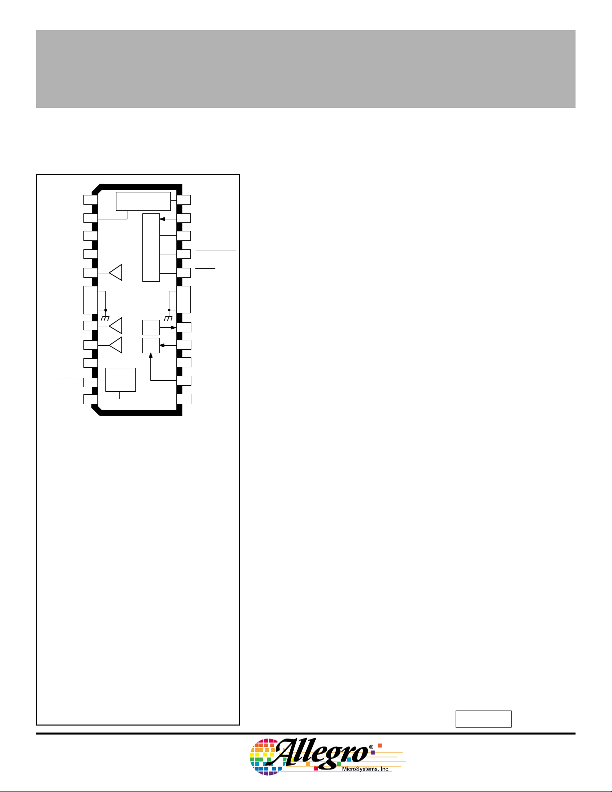
The A8906CLB is a bidirectional three-phase brushless dc motor
controller/driver. The three half-bridge outputs are low on-resistance nchannel DMOS devices capable of driving up to 1 A. The A8906CLB
provides complete, reliable, self-contained back-EMF sensing motor
startup and running algorithms. A programmable digital frequencylocked loop speed control circuit together with the linear current control
circuitry provides precise motor speed regulation.
A serial port allows the user to program various features and
modes of operation, such as the speed control parameters, rotational
direction, startup current limit, sleep mode, diagnostic modes, and
others.
The A8906CLB is fabricated in Allegro’s BCD (Bipolar CMOS
DMOS) process, an advanced mixed-signal technology that combines
bipolar, analog and digital CMOS, and DMOS power devices. The
A8906CLB is provided in a 24-lead wide-body SOIC batwing package.
It provides for the smallest possible construction in surface-mount
applications.
PRELIMINARY INFORMATION
FEATURES
■ DMOS Outputs
■ Low r
■ Startup Commutation Circuitry
■ Back-EMF Commutation Circuitry
■ Direction Control
■ Serial Port Interface
■ Frequency-Locked Loop Speed Control
■ Sector Data Tachometer Signal Input
■ Programmable Start-Up Current
■ Diagnostics Mode
■ Sleep Mode
■ Linear Current Control
■ Internal Current Sensing
■ Dynamic Braking Through Serial Port
■ Power-Down Dynamic Braking
■ System Diagnostics Data Out
■ Data Out Ported in Real Time
■ Internal Thermal Shutdown Circuitry
Always order by complete part number, e.g., A8906CLB .
DS(on)
(Subject to change without notice)
March 1, 1999
Data Sheet
26301.4
8906
BIDIRECTIONAL
3-PHASE BRUSHLESS DC
MOTOR CONTROLLER/DRIVER
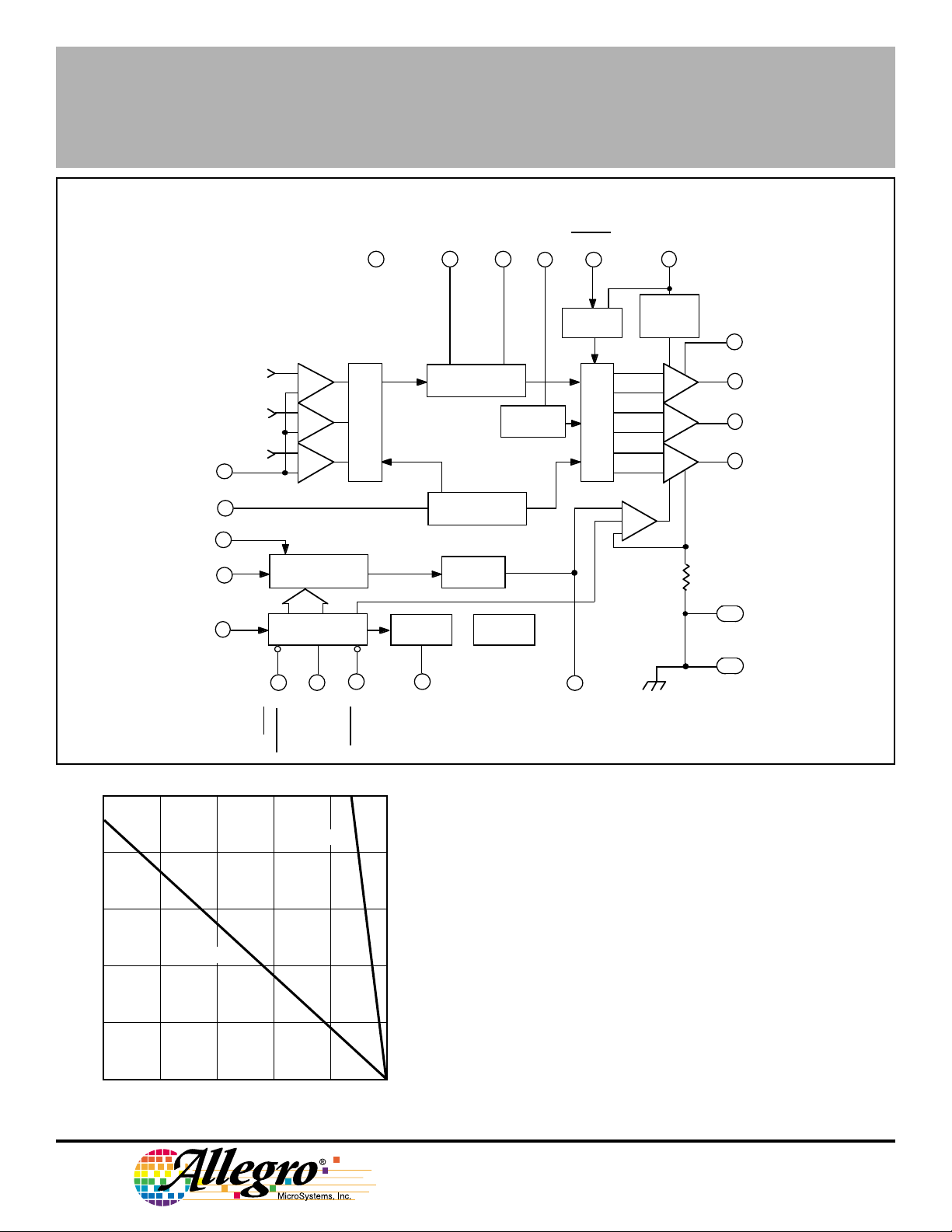
FUNCTIONAL BLOCK DIAGRAM
LOGIC
SUPPLY
15
V
DD
CENTERTAP
10
OUT
OUT
OUT
A
B
C
FCOM
LOGIC
BLANK
COMMUTATION
C
D1
24
C
D2
2
COMMUTATION
DELAY
START-UP
C
OSC.
4
ST
BRAKE
11
BRAKE
SEQUENCE
LOGIC
C
RES
12
BOOST
CHARGE
PUMP
V
BB
1
5
8
9
LOAD
SUPPLY
OUT
A
OUT
B
OUT
C
2.5
2.0
1.5
1.0
C
WD
SECTOR
DATA
OSC
DATA IN
R = 55°C/W
θJA
3
14
16
23
FREQUENCY-
LOCKED LOOP
SERIAL PORT MUX
22
21
WATCHDOG
CHARGE
1720
TIMER
PUMP
TSD
13
CURRENT
CONTROL
R
S
6-7
GROUND
18-19
GROUND
FILTER
CHIP
SELECT
R = 6°C/W
θJT
CLOCK
RESET
OUT
DATA
Dwg. FP-034
0.5
0
25
ALLOWABLE PACKAGE POWER DISSIPATION in WATTS
50 75 100 125 150
TEMPERATURE in °C
Dwg. GP-019B
115 Northeast Cutoff, Box 15036
Worcester, Massachusetts 01615-0036 (508) 853-5000
Copyright © 1999 Allegro MicroSystems, Inc.

8906
BIDIRECTIONAL
3-PHASE BRUSHLESS DC
MOTOR CONTROLLER/DRIVER
ELECTRICAL CHARACTERISTICS at T
= +25°C, V
A
= 5.0 V
DD
Limits
Characteristic Symbol Test Conditions Min. Typ. Max. Units
Logic Supply Voltage V
Logic Supply Current I
DD
DD
Operating 4.5 5.0 5.5 V
Operating — 7.5 10 mA
Sleep Mode — 250 500 µA
Load Supply Voltage V
Thermal Shutdown T
Thermal Shutdown Hysteresis ∆T
BB
J
J
Operating 4.0 — 14 V
— 165 — °C
— 20 — °C
Output Drivers
Output Leakage Current I
Total Output ON Resistance r
DSX
DS(on)
VBB = 14 V, V
V
= 14 V, V
BB
I
= 600 mA — 1.0 1.4 Ω
OUT
= 14 V — 1.0 300 µA
OUT
= 0 V — -1.0 -300 µA
OUT
(Source + Sink + RS)
Output Sustaining Voltage V
DS(sus)
Clamp Diode Forward Voltage V
F
V
= 14 V, I
BB
OUT
= I
(MAX), L = 3 mH 14 ——V
OUT
IF = 1.0 A — 1.25 1.5 V
Control Logic
Logic Input Voltage V
Logic Input Current I
DATA Output Voltage V
C
Current I
ST
C
Threshold V
ST
Filter Current I
Filter Threshold V
CD Current I
IN(0)
V
IN(1)
IN(0)
I
IN(1)
OUT(0)
V
OUT(1)
CST
CSTH
V
CSTL
FILTER
FILTERTH
CD
(CD1 or CD2)
C
Current Matching — I
D
CD Threshold V
CDTH
SECTOR DATA, RESET, CLK, -0.3 — 1.5 V
CHIP SELECT, OSC 3.5 — 5.3 V
VIN = 0 V ——-0.5 µA
VIN = 5.0 V ——1.0 µA
I
= 500 µA ——1.5 V
OUT
I
= -500 µA 3.5 —— V
OUT
Charging -9.0 -10 -11 µA
Discharging — 500 — µA
2.25 2.5 2.75 V
0.85 1.0 1.15 V
Charging -9.0 -10 -11 µA
Discharging 9.0 10 11 µA
Leakage, V
= 2.5 V ——5.0 nA
FILTER
1.57 1.85 2.13 V
Charging -18 -20 -22 µA
Discharging 32 40 48 µA
CD(DISCHRG)/ICD(CHRG)
1.8 2.0 2.2 —
2.25 2.5 2.75 V
Continued next page …
8906
BIDIRECTIONAL
3-PHASE BRUSHLESS DC
MOTOR CONTROLLER/DRIVER
ELECTRICAL CHARACTERISTICS continued
Limits
Characteristic Symbol Test Conditions Min. Typ. Max. Units
C
Current I
WD
C
Threshold Voltage V
WD
Max. FLL Oscillator Frequency f
I
(MAX) — D3 = 0, D4 = 0 1.0 1.2 1.4 A
OUT
CWD
V
TH
OSC
TL
Charging -9.0 -10 -11 µA
0.22 0.25 0.28 V
2.25 2.5 2.75 V
VDD = 5.0 V, TA = 25°C12——MHz
D3 = 0, D4 = 1 0.9 1.0 1.1 A
D3 = 1, D4 = 0 0.5 0.6 0.7 A
D3 = 1, D4 = 1 — 250 — mA
BRAKE Threshold V
BRAKE Hysteresis Current I
Transconductance Gain g
Centertap Resistors R
BRK
BRKL
m
CT
Back-EMF Hysteresis — V
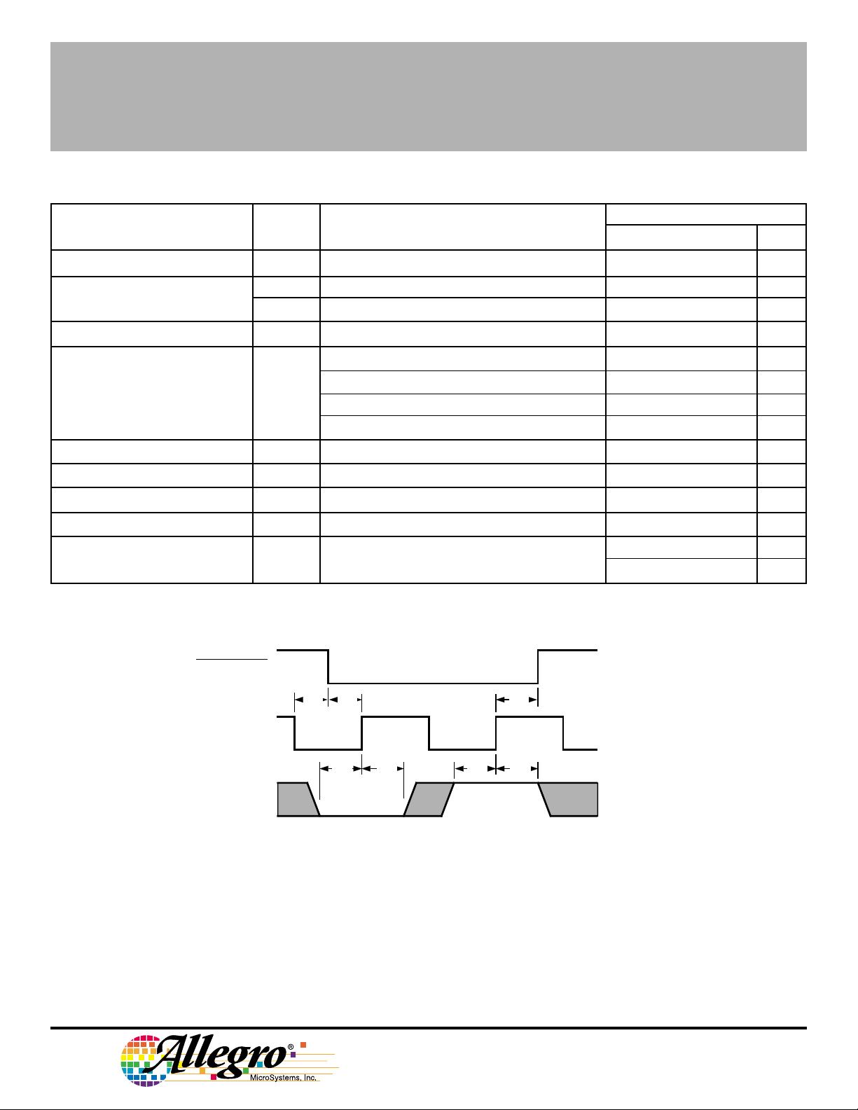
SERIAL PORT TIMING CONDITIONS
CHIP SELECT
E
CLOCK
DATA
1.5 1.75 2.0 V
V
= 750 mV — 20 — µA
BRK
0.42 0.50 0.58 A/V
5.0 10 13 kΩ
BEMF
- V
at 5.0 20 37 mV
CTAP
FCOM Transition -5.0 -20 -37 mV
A
C
D C D
B
Dwg. WP-019
A. Minimum CHIP SELECT setup time before CLOCK rising edge.......... 100 ns
B. Minimum CHIP SELECT hold time after CLOCK rising edge............... 150 ns
C. Minimum DATA setup time before CLOCK rising edge........................ 150 ns
D. Minimum DATA hold time after CLOCK rising edge............................. 150 ns
E. Minimum CLOCK low time before CHIP SELECT.................................. 50 ns
F. Maximum CLOCK frequency .............................................................. 3.3 MHz
115 Northeast Cutoff, Box 15036
Worcester, Massachusetts 01615-0036 (508) 853-5000
 Loading...