

Page 1
A8601
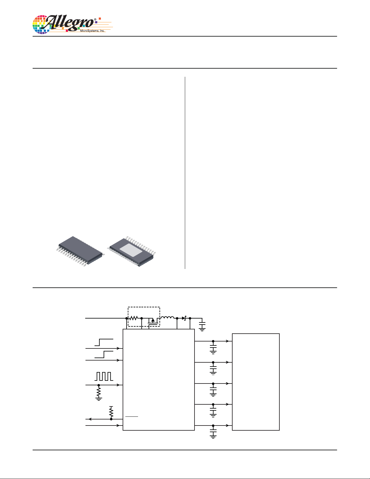
Multiple-Output Regulator for Automotive LCD Displays
Features and Benefits
• Automotive Grade AEC-Q100 qualified
• Five individual output supplies
• Independent control of each output voltage
• 350 kHz to 2.25 MHz switching frequency with external
synchronization capability
• <10 μA shutdown current
• Preprogrammed power-up and shutdown sequences
• Overcurrent, overvoltage, short circuit, and thermal
overload protection
Applications:
• GPS
• Infotainment
• Medium LCDs
Package: 28-pin TSSOP with exposed
thermal pad (suffix LP)
Description
The A8601 is a fixed frequency, multiple-output supply for
LCD bias. Its switching frequency can be either programmed
or synchronized with an external clock signal between 350 kHz
and 2.25 MHz, to minimize interference with AM and FM
radio bands.
A total of five output voltages are provided, from three linear
regulators and two charge-pump regulators. Each output
voltage can be adjusted independently. During power-up and
shutdown, the outputs are turned on and off in preprogrammed
sequences, to meet the sequencing requirements for specific
LCD panels.
Short circuit protection is provided for all outputs. The boost
switch is protected against overcurrent and overvoltage. Input
disconnect protection is achieved by driving an external
P-MOSFET.
28-pin exposed thermal pad TSSOP package allows operation
at high ambient temperatures. It is lead (Pb) free with 100%
matte-tin leadframe plating.
Not to scale
VIN
External Sync
1.5 to 3.2 V
System Block Diagram
Optional
R
SC
Q1
INS GATE SW
VIN
EN1
EN2
FSET_SYNC
V
VIN
FAULT
VINAMP
A8601
D1L1
OUT
DVDD
AVDD
VGH
VGL
VCOM
V
DVDD
V
AVDD
V
VGH
V
VGL
V
VCOM
3.3 V
5 to 14 V
LCD Panel
10 to 25 V
+
– 5 to –12 V
+
3 to 6 V
+
Output voltages shown are
for typical LCD Panel
A8601-DS, Rev. 1
Page 2
A8601
Multiple-Output Regulator for Automotive LCD Displays
Selection Guide
Part Number Packing* Programming
A8601KLPTR-T 4000 pieces per 13-in. reel
*Contact Allegro
®
for additional packing options.
Contact Allegro Sales for
VCOM regulator factory trim option
Absolute Maximum Ratings
1,2
Characteristic Symbol Notes Rating Unit
VIN and INS Pin Voltage V
SW Pin Voltage
3,4
VIN
V
OUT Pin Voltage V
AVDD and FB2 Pin Voltage V
AVDD
CP11 Pin Voltage V
CP12 Pin Voltage V
VGH Pin Voltage V
FB4 Pin Voltage V
CP21 Pin Voltage V
V
V
CP22
EN1
V
V
CP22, VGL and FB3 Pin Voltage
EN1, EN2, and ¯F¯ ¯A
¯¯¯U ¯¯L¯ ¯T¯
Pin Voltage
BIAS Pin Voltage V
VCOM Pin Voltage V
V
PGND and GNDVCOM Pin Voltage
All other pins
5
PGND
V
GNDVCOM
Operating Ambient Temperature T
, V
SW
OUT
, V
CP11
CP12
VGH
FB4
CP21
, V
FB3
, V
FAULT
BIAS
VCOM
– –0.3 to 7 V
A
All voltages measured with respect to GND –0.3 to 6.5 V
INS
Continuous –0.6 to 22 V
Voltage spikes (pulse width < 100 ns) –1 to 40 V
–0.3 to 22 V
FB2
Positive charge pump
–0.3 to
V
OUT
–0.3 to
V
CP12
Positive charge pump –0.3 to 27 V
Positive charge pump –0.3 to 27 V
Positive charge pump
–0.3 to
V
VGH
Negative charge pump –0.3 to 14 V
,
VGL
Negative charge pump –14 to 0.3 V
,
EN2
–0.3 to 5.5 V
–0.3 to lower of:
5.5 or V
–0.3 to lower of:
7 or V
AVDD
,
–0.3 to 0.3 V
K temperature range –40 to 125 ºC
+ 0.3
+ 0.3
+ 0.3
VIN
+ 0.3
+ 0.3
V
V
V
V
V
Maximum Junction Temperature TJ(max) 150 ºC
Storage Temperature T
1
Stresses beyond those listed in this table may cause permanent damage to the device. The Absolute Maximum ratings are stress ratings
stg
–55 to 150 ºC
only, and functional operation of the device at these or any other conditions beyond those indicated in the Electrical Characteristics table is
not implied. Exposure to Absolute Maximum-rated conditions for extended periods may affect device reliability.
2
All voltages referenced to AGND.
3
The SW pin has internal clamp diodes to GND. Applications that forward bias this diode should take care not to exceed the IC package
power dissipation limits. Note: Exact energy specification to be determined.
4
The switch DMOS is self-protected. If voltage spikes exceeding 40 V are applied, the device would conduct and absorb the energy safely.
5
When V
= 0 (no power), all inputs are limited by -0.3 to 5.5 V.
VIN
Thermal Characteristics may require derating at maximum conditions, see application information
Characteristic Symbol Test Conditions* Value Unit
Package Thermal Resistance
*Additional thermal information available on the Allegro website.
R
θJA
On 4-layer PCB based on JEDEC standard 28 ºC/W
Allegro MicroSystems, Inc.
115 Northeast Cutoff
Worcester, Massachusetts 01615-0036 U.S.A.
1.508.853.5000; www.allegromicro.com
2
Page 3

A8601
Multiple-Output Regulator for Automotive LCD Displays
Table of Contents
Characteristic Performance 10
Functional Description 15
Linear Regulators 15
VCOM Regulator 15
Charge Pumps 16
Boost Controller 18
Switching Frequency 19
Continuous Conduction Mode Operation 20
Input Disconnect Switch 21
FAULT Conditions 22
Pre-Output Fault Detection 23
General Fault Detection 23
Application Information 24
Output Voltage Selection 24
Output Capacitance 25
Operating with Separate VIN and
Boost Supplies 26
Thermal Analysis 26
Component Selection Recommendations 28
I/O pin Equivalent Circuit Diagrams 29
Allegro MicroSystems, Inc.
115 Northeast Cutoff
Worcester, Massachusetts 01615-0036 U.S.A.
1.508.853.5000; www.allegromicro.com
3
Page 4
A8601
Multiple-Output Regulator for Automotive LCD Displays
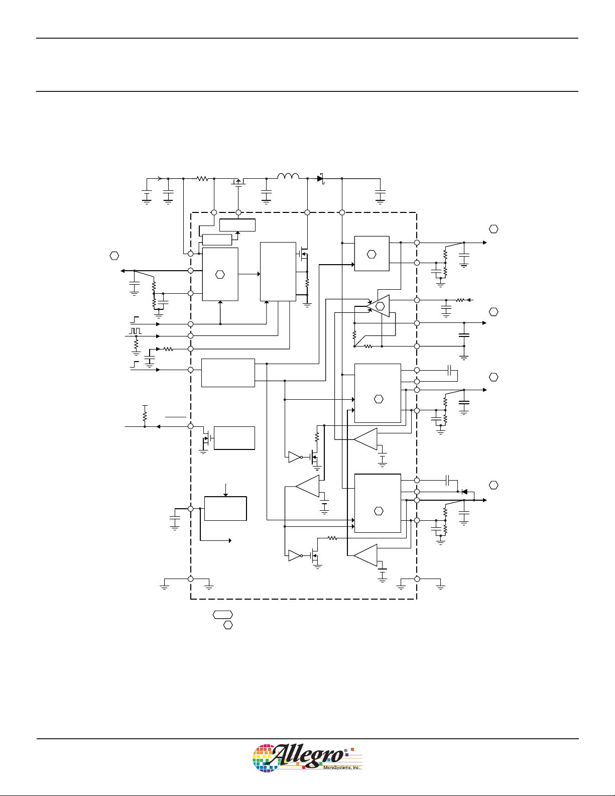
Functional Block Diagram
5 V DC to DC
Converter
(
4V )
min.
6
V
DVDD
3.3V
External
.
Sync
FSET_SYNC
C
COMP
V
VIN
FAULT
VIN
DVDD
FB1
EN1
COMP
EN2
R
INS
SC
OCP
LDO
1
Enable/
Disable
Fault
Q1
Drive
GATE
REG
Boost
Regulator
with
Soft
Start
SW
OFF
OFF
ON
OFF
D1L1
ON
OFF
ON
ON
OUT
X1.9 4
OP AMP
ON
+
LDO
2
+
5
2x
Charge
Pump
4
–
–
90%
C
OUT
6
+
C
Microprocessor
+
C
+
V
AVDD
10V
AVDD
1.5 to 3.2 V
from
6
V
VCOM
3 to6 V
VCOM
6
V
VGH
18 V
AVDD
FB2
VINAMP
VCOM
GNDVCOM
C
FLY1
CP11
CP12
VGH
FB4
BIAS
AGND
V
IN
BIAS
Regulat or
3.6 V
See Terminal List Table
1 to 5
6
Output voltages shown are for a typic
ON
OFF
OFF
C
FLY2
+
10%
-
Inverted
Charge
Pump
3
+
–
al LCD panel
90 %
CP21
CP22
VGL
FB
3
+
PGND
Allegro MicroSystems, Inc.
115 Northeast Cutoff
Worcester, Massachusetts 01615-0036 U.S.A.
1.508.853.5000; www.allegromicro.com
V
-8 V
6
VGL
4
Page 5
A8601
Multiple-Output Regulator for Automotive LCD Displays
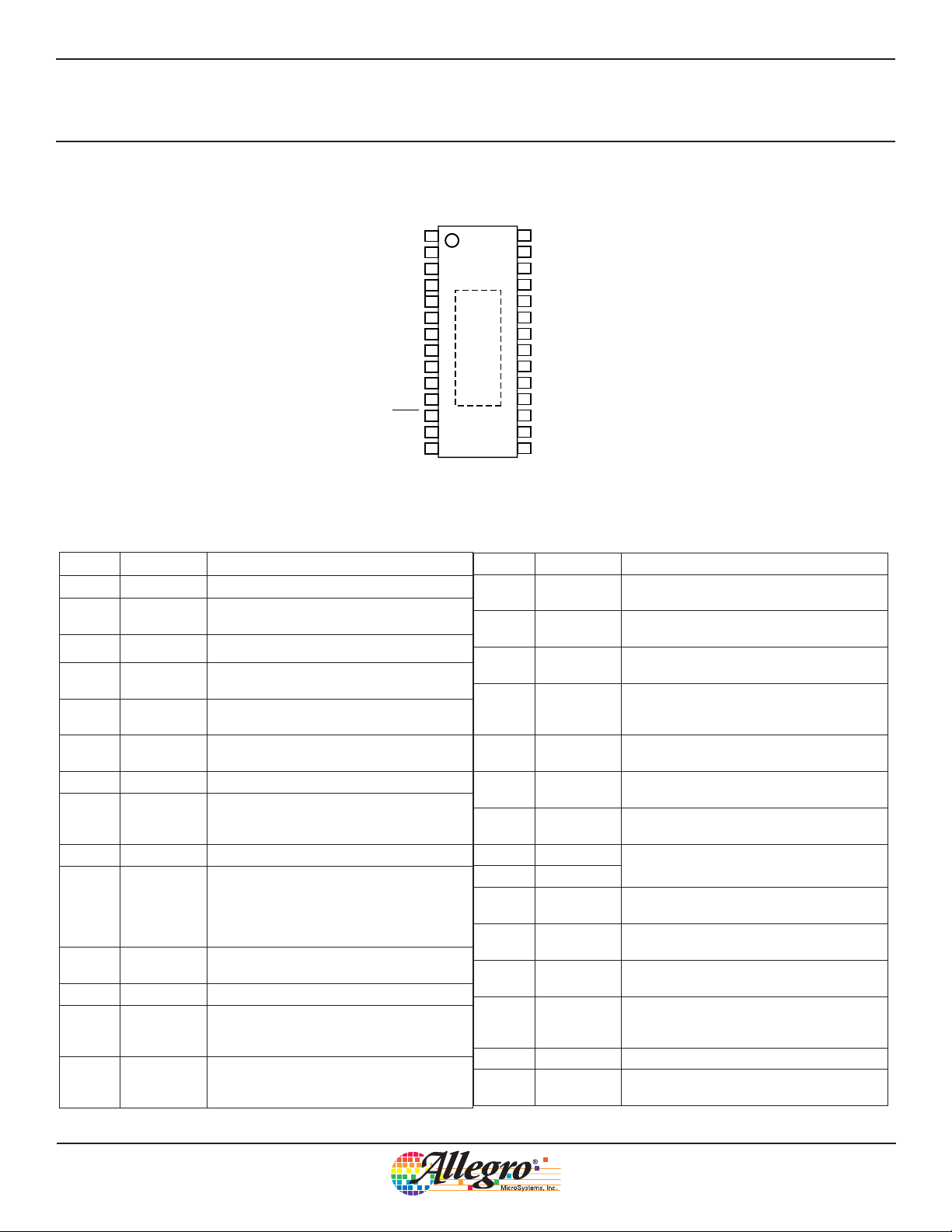
Pin-out Diagram
GATE
INS
VIN
DVDD
FB1
COMP
VINAMP
VCOM
GNDVCOM
FSET_SYNC
BIAS
FAULT
EN1
EN2
Terminal List Table
Number Name Function
1 GATE Gate driver for input disconnect P-MOSFET
2 INS
3 VIN Input supply voltage (4.0 to 5.5 V) for the IC
4 DVDD
5
FB1
(DVDD)
6 COMP
7 VINAMP Control voltage from external microprocessor
8 VCOM
9 GNDVCOM Ground reference for VCOM
10 FSET_SYNC
11 BIAS
12 ¯F¯ ¯A
¯¯¯U ¯¯L¯ ¯T¯
13 EN1
14 EN2
High-side sense for input overcurrent
detection
Output from internal LDO (item 1 in Functional
Block Diagram) powered by VIN
Connect to resistor divider network to set
DVDD
Compensation pin, connect to external COMP
capacitor
Output from operational amplifier (item 5 in
Functional Block Diagram), controlled by
VINAMP
Input for synchronizing boost and charge
pump signals switching frequency to external
clock signal; alternatively, it can be connected
to an external resistor to set the switching
frequency
Output from internal 3.6 V bias regulator;
connect to GND via 0.1 μF ceramic capacitor
Open-drain output, pulls low in error condition
Enable pin for DVDD output; system can only
be enabled after V
(refer to Startup Timing Diagram)
is above UVLO level
VIN
Enable pin for the voltage outputs other than
DVDD; it can be activated only after V
above UVLO and EN1 = high.
VIN
28
1
2
3
4
5
6
PAD
7
8
9
10
11
12
13
14
SW
27
PGND
26
OUT
25
AVD D
24
FB2
23
CP11
22
CP12
21
VGH
20
FB4
19
CP21
18
CP22
17
VGL
16
FB3
15
AGND
Number Name Function
15 AGND
16
FB3
(VGL)
17 VGL
Analog GND reference for signals; connect to
ground plane
Connect to resistor divider network to set V
VGL
Inverted charge pump output
(item 3 in Functional Block Diagram)
Capacitor terminal for inverted charge pump
18 CP22
(item 3 in Functional Block Diagram); refer to
Negative Charge Pump section for usage
19 CP21
20
FB4
(VGH)
21 VGH
22 CP12
23 CP11
24
FB2
(AVDD)
25 AVDD
26 OUT
Capacitor terminal for inverted charge pump
(item 3 in Functional Block Diagram)
Connect to resistor divider network to set V
VGH
2x charge pump (item 4 in Functional Block
Diagram) output
Capacitor terminals for charge pump
(item 4 in Functional Block Diagram)
Connect to external resistor network to set
V
AVDD
Output from internal LDO (item 2 in Functional
Block Diagram) powered by V
OUT
Connect to boost output for internal LDO and
charge pump regulators
Power ground for internal boost switch;
27 PGND
connect this pin to ground terminal of
output ceramic capacitor(s)
28 SW Boost converter switch node
is
– PAD
Exposed pad (substrate of IC); solder to GND
plane for better thermal conduction
Allegro MicroSystems, Inc.
115 Northeast Cutoff
Worcester, Massachusetts 01615-0036 U.S.A.
1.508.853.5000; www.allegromicro.com
5
Page 6
A8601
Multiple-Output Regulator for Automotive LCD Displays
ELECTRICAL CHARACTERISTICS
V
= –8 V, TJ = TA = 25°C, except indicates specifications guaranteed for TJ = TA = −40°C to 125°C; unless otherwise specified
VGL
1
Valid at V
= 5 V, EN1 = EN2 = high, fSW = 2 MHz, V
VIN
DVDD
= 3.3 V, V
AVDD
= 10 V, V
Characteristics Symbol Test Conditions Min. Typ. Max. Unit
Input Voltage and Current
Input Voltage V
VIN Pin Undervoltage Lockout
(UVLO) Threshold
VIN Pin UVLO Hysteresis V
Shutdown Bias Current I
Standby Bias Current I
Operating Bias Current I
V
UVLO(HYS)
VINBIAS(SD)
VINBIAS(STB)
VINBIAS(OP)
VIN
UVLO
V
rising 3.6 – 4.0 V
VIN
Current into VIN pin, EN1 = low –550μA
EN1 = high, EN2 = low, no load at DVDD pin – 2 – mA
EN1 = high, EN2 = high – 6.5 – mA
4.0 – 5.5 V
– 0.15 0.25 V
Boost Switch
Switch Peak Current Limit I
Switch On-Resistance R
Switch Minimum On-Time t
Switch Minimum Off-Time t
SW Pin Leakage Current I
OUT Pin Leakage Current I
SW Pin Secondary Overvoltage
Protection (OVP)
SW Pin Secondary OVP Minimum
Pulse Width
4
V
t
SW(MAX)
DS(on)ISW
ON(MIN)
OFF(MIN)
SW(LKG)VSW
OUT(LKG)VOUT
SW(OVP)
SW(OVP)VSW
Cycle-by-cycle current limit 1.3 – 2.0 A
= 0.5 A – 0.5 – Ω
50 72 95 ns
33 50 75 ns
= 5 V, EN1 = low – 0.1 – μA
= 5 V, EN1 = low – 0.1 – μA
17.4 19.2 21.2 V
≥ OVP level – 40 – ns
Switching Frequency / Synchronization
FSET_SYNC Pin Voltage V
FSET_SYNC Pin Current I
FSETSYNC
FSETSYNC
Switching Frequency f
Synchronization Frequency f
Synchronization Minimum On-Time t
Synchronization Minimum Off-Time t
SYNC(ON)
SYNC(OFF)
SW
SYNC
Without using external synchronization signal
R
FSET_SYNC
= 5.1 kΩ 1.81 2.0 2.17 MHz
External logic signal connected to
FSET_SYNC pin
– 1.0 – V
34 – 220 μA
0.35 – 2.25 MHz
150 – – ns
150 – – ns
Input Disconnect
= V
GATE Pin Sink Current I
GATE Pin Source Current I
GATE Voltage at Off Condition V
INS Trip Point V
INS Trip Blanking Time t
GATE(SNK)VGATE
GATE(SRC)VGATE
GATE(OFF)
INS(TRIP)
INS(BLANK)
EN1 = EN2 = low, or fault tripped – V
Between VIN and INS pins 85 100 115 mV
Sensed voltage = 2 × input current limit 1.5 – 3 μs
, no fault – 100 – μA
VIN
= 0 V, fault tripped – 130 – mA
VIN
= 20 V,
VGH
–V
Continued on the next page…
Allegro MicroSystems, Inc.
115 Northeast Cutoff
Worcester, Massachusetts 01615-0036 U.S.A.
1.508.853.5000; www.allegromicro.com
6
Page 7
A8601
Multiple-Output Regulator for Automotive LCD Displays
ELECTRICAL CHARACTERISTICS
V
= 20 V, V
VGH
otherwise specified
Feedback Pins
Feedback Sense Voltage V
Output Overvoltage Fault Threshold V
Output Undervoltage Fault Threshold V
Feedback Input Currents I
Feedback Load Resistance
Output Regulators
DVDD Output Voltage V
AVDD Output Voltage V
VCOM Output Voltage V
VGH Output Voltage V
VGL Output Voltage V
Dropout for DVDD Regulator V
Boost Minimum Headroom for AVDD
Regulator
Boost Minimum Headroom for VGH
Regulator
Boost Minimum Headroom for VGL
Regulator
Output Pull-Down Resistor During
Shutdown (AVDD, VCOM, VGH, VGL)
Logic Inputs
Input Logic High V
Input Logic Low V
Internal Pull-Down Resistance to AGND R
= –8 V, TJ = TA = 25°C, except indicates specifications guaranteed for TJ = TA = −40°C to 125°C; unless
VGL
Characteristics Symbol Test Conditions Min. Typ. Max. Unit
2
V
V
V
R
1
(continued) Valid at V
FB1, FB2, and FB4 pins – 2.40 – V
FBx
FB3 pin – –1.8 – V
FB1, FB2, and FB4 pins; V
FBx(OV)
V
falling – –2.16 – V
FB3
FB1, FB2, and FB4 pins; V
FBx(UV)
V
rising – –1.44 – V
FB3
FB1, FB2, and FB4 pins; V
FBx
V
= –1.8 V – 0.5 – μA
FB3
FB1 pin 9 10 11 kΩ
R
FB2 pin 24 25 26 kΩ
FBx
FB3 and FB4 pins 49 50 51 kΩ
DVDDVVIN
AVDD
VCOMVVIN
VGH
VGL
DVDD(DO)
AVDD(DO)
VGH(DO)
VGL(DO)
OUTPD
IH
IL
ENx(PD)
= 4.0 to 5.5 V 2.4 – V
V
= 4.0 to 5.5 V 4.4 – 14.8 V
VIN
= 4.0 to 5.5 V, V
V
= 4.0 to 5.5 V 2.4 – 26 V
VIN
V
= 4.0 to 5.5 V –12.9 – –5 V
VIN
Between VIN and DVDD pins;
V
= 2.33 V, I
FB1
Defined as V
I
= 100 mA
OUT
Defined as V
V
= 2.33 V, I
FB4
Defined as V
= –1.75 V, I
V
FB3
EN1 = high, EN2 = low – 250 – Ω
EN1, EN2, FSET_SYNC pins 1.8 – – V
EN1, EN2, FSET_SYNC pins – – 0.8 V
EN1, EN2 pins – 100 – kΩ
OUT
OUT
OUT
= 5 V, EN1 = EN2 = high, fSW = 2 MHz, V
VIN
rising – 2.88 – V
FBx
falling – 1.92 – V
FBx
= 2.4 V – –0.5 – μA
FBx
OUT
– V
– V
OUT
– (–V
OUT
> V
AVDD
= 50 mA
; V
AVDD
/ 2;
VGH
= 8 mA
VGL
= –8 mA
);
+ 1.5 V 2.9 – 6.8 V
VCOM
= 2.33 V,
FB2
DVDD
= 3.3 V, V
VIN
= 10 V,
AVDD
– 0.6 V
– – 0.6 V
–2–V
– 2.4 – V
– 3.6 – V
Continued on the next page…
Allegro MicroSystems, Inc.
115 Northeast Cutoff
Worcester, Massachusetts 01615-0036 U.S.A.
1.508.853.5000; www.allegromicro.com
7
Page 8
A8601
Multiple-Output Regulator for Automotive LCD Displays
ELECTRICAL CHARACTERISTICS
V
= 20 V, V
VGH
otherwise specified
Output Current Capacity
DVDD Overcurrent Protection (OCP)
Trip Level
AVDD OCP Trip Level I
VCOM OCP Trip Level i
VGH OCP Trip Level i
VGL OCP Trip Level i
Output Voltage Accuracy
DVDD Load Regulation V
AVDD, VGL and VGH Load
Regulation
DVDD Accuracy
AVDD Accuracy
VGH Accuracy
VGL Accuracy
VCOM Operational Amplifier
VCOM Gain
VCOM Load Regulation
VCOM Temperature Coefficient
Input Resistance to AGND R
Dropout for VCOM from AVDD V
¯F¯ ¯
¯¯¯U ¯¯L¯ ¯T¯
A
Pin
¯F¯ ¯
¯¯¯U ¯¯L¯ ¯T¯
A
Pull-Down Voltage V
¯F¯ ¯
¯¯¯U ¯¯L¯ ¯T¯
A
Pin Leakage Current V
= –8 V, TJ = TA = 25°C, except indicates specifications guaranteed for TJ = TA = −40°C to 125°C; unless
VGL
Characteristics Symbol Test Conditions Min. Typ. Max. Unit
I
DVDD(OCP)
AVDD(OCP)
3
3
3
3
4
4
4
err
err
V
TC
VINAMP(PD)
VCOM(DO)VAVDD
FAULT(PD)
FAULT(LKG)
1
(continued) Valid at V
Includes i
VCOM
VGH
VGL
DVDDregVDVDD
V
err
err
Current into VGL pin 14 – 32 mA
xregILOAD
DVDDVDVDD
AVDDVAVDD
VGHVVGH
V
VGL
VCOM
= 3.3 V, I
= 10% to 100% of I
= 3.30 V –2.5 – 2.5 %
= 10.0 V –2.1 – 2.1 %
= 20.0 V –2.5 – 2.5 %
= –8.0 V –2.5 – 2.5 %
VGL
Defined as V
A
VCOM
VCOMregILOAD
1.5 V < V
85°C, I
–30°C < TA < 85°C, I
VCOM
VINAMP
LOAD
= 5 to 50 mA –5 – 5 mV
VINAMP pin – 100 – kΩ
= 7 V, I
Fault condition asserted,
pull-up current = 1 mA
Fault condition cleared, pull-up to 5 V – – 1 μA
= 5 V, EN1 = EN2 = high, fSW = 2 MHz, V
VIN
DVDD
= 3.3 V, V
50 – 90 mA
200 – 350 mA
60 – 110 mA
14 – 32 mA
= 10 to 50 mA –0.1 – 0.1 V
LOAD
(min) –0.1 – 0.1 V
x(OCP)
/ V
VCOM
< 3.21 V, –30°C < TA <
VINAMP
;
1.92 1.94 1.96 V / V
= 25 mA
= 25 mA –50 – 50 μV/°C
LOAD
= 60 mA – – 1.5 V
VCOM
– – 0.4 V
AVDD
= 10 V,
Continued on the next page…
Allegro MicroSystems, Inc.
115 Northeast Cutoff
Worcester, Massachusetts 01615-0036 U.S.A.
1.508.853.5000; www.allegromicro.com
8
Page 9
A8601
Multiple-Output Regulator for Automotive LCD Displays
ELECTRICAL CHARACTERISTICS
V
VGH
= 20 V, V
= –8 V, TJ = TA = 25°C, except indicates specifications guaranteed for TJ = TA = −40°C to 125°C; unless
VGL
1
(continued) Valid at V
= 5 V, EN1 = EN2 = high, fSW = 2 MHz, V
VIN
DVDD
= 3.3 V, V
AVDD
otherwise specified
Characteristics Symbol Test Conditions Min. Typ. Max. Unit
Fault Timers
Soft Start Time-Out t
SS(TO)
Maximum time allowed for any output to
reach 90% of its target
Maximum time allowed for VGH to fall to
Shutdown Time-Out t
Overcurrent Protection (OCP)
Time-Out
Restart Delay t
t
RESTART
Fault Counter Reset Time t
SDN(TO)
OCP(TO)
fault
10% and VGL to 30% of their respective
targets; EN1 = high, EN2 = low
Maximum time allowed for any output to
stay in an overcurrent fault condition before
shutdown
Delay time after fault shutdown until the next
retry (repeats until Fault counter = 8)
Time required after setting EN1 = low until
Fault counter clears
Thermal Shutdown (TSD) Protection
TSD Threshold T
TSD Hysteresis
1
For input and output current specifications, negative current is defined as coming out of the node or pin (sourcing), positive current is defined as
going into the node or pin (sinking).
2
Net parallel resistance required at FBx pin in order to meet accuracy.
3
Output voltage is set to required nominal value using external sense resistor network. Output current at 50% of minimum OCP trip level. Accuracy
does not include mismatch error caused by external sense resistor network.
4
Ensured by design and characterization, not production tested.
4
T
TSD(HYS)
Temperature rising – 165 – °C
TSD
40 50 60 ms
40 50 60 ms
40 50 60 ms
80 100 120 ms
1––μs
–20–°C
= 10 V,
Allegro MicroSystems, Inc.
115 Northeast Cutoff
Worcester, Massachusetts 01615-0036 U.S.A.
1.508.853.5000; www.allegromicro.com
9
Page 10
A8601
Multiple-Output Regulator for Automotive LCD Displays
Characteristic Performance
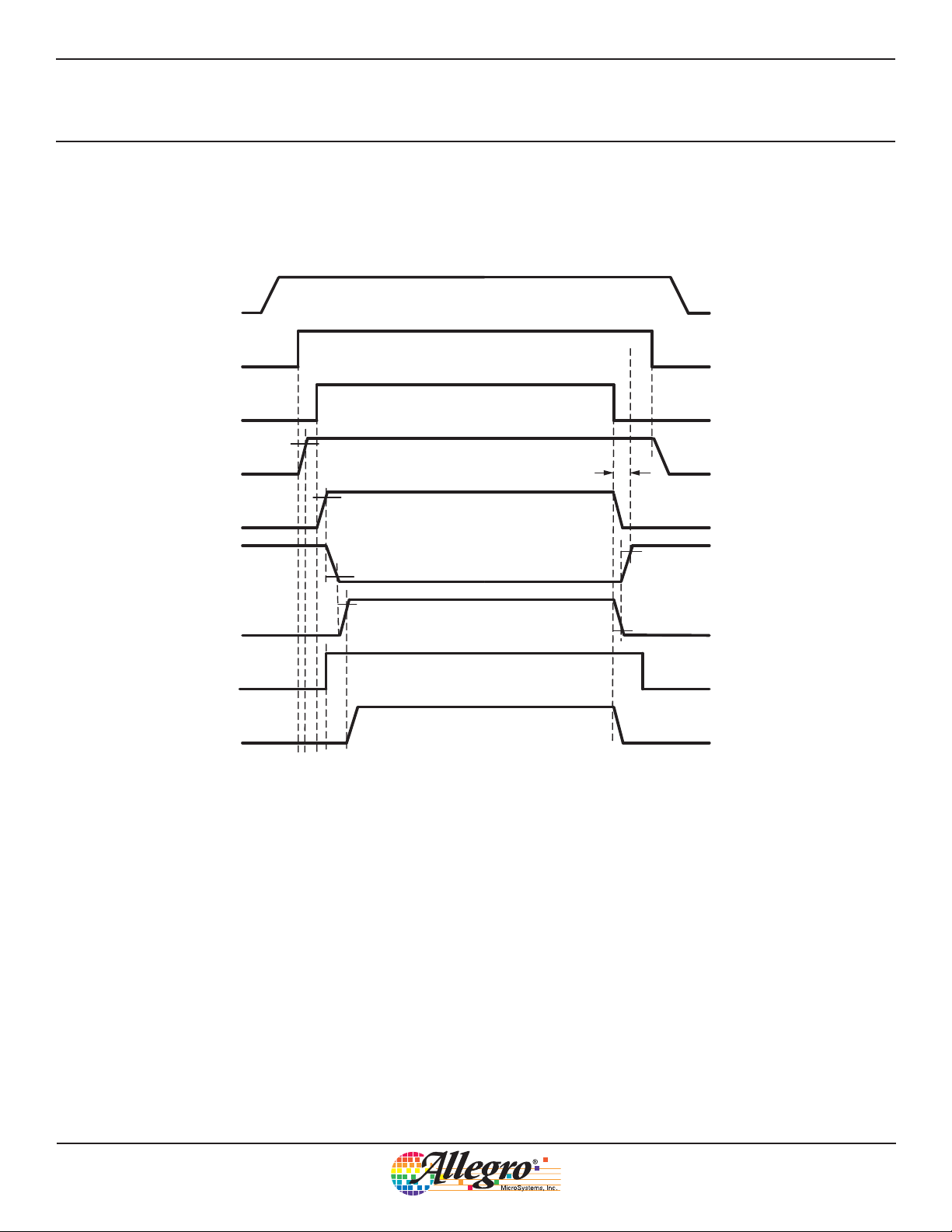
Startup and Shutdown Sequences (Normal Operation)
VIN
EN1
EN2
DVDD
AVDD
VGL
VGH
90%
t<100 ms
90%
30%
90%
90%
10%
VINAMP
VCOM
Notes:
• Normal system startup should follow the above sequence (VIN → EN1 → EN2).
• EN1 can only be asserted after VIN is above UVLO level, V
ignored until VIN rises above V
• EN2 can only be asserted when DVDD is >90% target voltage. If asserted before that, it is ignored
until the condition is met.
• VGH is enabled only after the magnitude of VGL has reached >90% of its target voltage.
• VCOM output is enabled only after VGH has reached >90% of its target voltage. (A valid VINAMP
must be asserted prior to this.)
• System shutdown should start with EN2 = low, followed by EN1 = low.
• VGL shutdown can only start after VGH has dropped to 10% its original target voltage, or the VGH
shutdown time-out interval has expired.
• EN1 = low can only be asserted when VGL has fallen below 30% of its target voltage. If asserted
before that, it is ignored until the condition is met or the VGL shutdown time-out interval has
expired.
UVLO
.
. If asserted before that, it is
UVLO
Allegro MicroSystems, Inc.
115 Northeast Cutoff
Worcester, Massachusetts 01615-0036 U.S.A.
1.508.853.5000; www.allegromicro.com
10
Page 11

A8601
VIN
Multiple-Output Regulator for Automotive LCD Displays
Startup and Shutdown Sequences (Irregular)
V
VIN
UVL O
VIN
EN1
EN2
DVDD
AVDD
VGL
VGH
VINAMP
VCOM
90%
90%
90%
90%
EN1
EN2
DVDD
AVDD
VGL
VGH
VINAMP
VCOM
90%
90%
90%
90%
EN1
EN2
DVDD
AVDD
VGL
VGH
VINAMP
VCOM
30%
10%
Case 1 (startup) Case 2 (startup) Case 3 (shutdown)
Notes:
• Case 1 (startup). During a startup sequence, if EN2 goes high before EN1 goes high, EN2 is
ignored until EN1 also goes high and DVDD has risen to 90% of its target voltage.
• Case 2 (startup). During a startup sequence, while VIN is below the UVLO level, V
in sleep mode. If either EN1 or EN2 goes high while the IC is still in sleep mode, they are ignored
until VIN exceeds V
UVLO
.
UVLO
, the IC is
• Case 3 (shutdown). During a shutdown sequence, if EN1 goes low before EN2 goes low, EN1
is ignored until EN2 also goes low and VGL has fallen to 30% of its target voltage, or the VGL
shutdown time-out interval has expired.
Allegro MicroSystems, Inc.
115 Northeast Cutoff
Worcester, Massachusetts 01615-0036 U.S.A.
1.508.853.5000; www.allegromicro.com
11
Page 12

A8601
Multiple-Output Regulator for Automotive LCD Displays
Startup Timing Diagram
>100 μs (determined by GATE pin capacitance)
IC waits until GATE pin < (V
– 3.5 V)
VIN
EN1
DVDD
EN2
AVDD
VGL
VGH
VCOM
≈ 4 ms for 48 μF
capacitor loading
12 ms for typical
≈
capacitor loading
EN2 ignored
≈
capacitor loading
90%
3 ms for 48 μF
4 ms for 24 μF
≈
capacitor loading
90%
≈
4 ms for 10 μF
capacitor loading
≈
2 ms for 10 μF
capacitor loading
EN1 ignored
90%
90%
90%
Notes:
• Startup ramps are based on internal timing and are assumed to have ± 20% variation.
• An internal pull-down resistor of 250 Ω is applied to each of the regulator outputs AVDD, VGL,
VGH, and VCOM as soon as EN1 = high. That means if any output capacitor was previously
charged, it would be discharged by this pull-down resistor. The pull-down is removed just
before each regulator is enabled.
Allegro MicroSystems, Inc.
115 Northeast Cutoff
Worcester, Massachusetts 01615-0036 U.S.A.
1.508.853.5000; www.allegromicro.com
12
Page 13

A8601
EN2
AVDD
VCOM
VGH
Multiple-Output Regulator for Automotive LCD Displays
Shutdown Timing Diagram
≈22 ms for 40 μF
capacitor discharge
10%
≈6 ms for 10 μF
capacitor discharge
10%
≈6 ms for 10 μF
capacitor discharge
10%
VGL
EN1
EN1 ignored
30%
7 ms for 24 μF
≈
capacitor discharge
Cumulative ≈
for 10 μF on VGH and 24 μF on VGL
EN1 active after AVDD, VGH, and VCOM
decay to <10%, and VGL decays to <30%,
of their target values
13 ms capacitor discharge
DVDD
Device enters
sleep mode
Notes:
• All exponential decays are based on external capacitance and internal pull-down resistance
(250 Ω each for AVDD, VCOM, VGH, and VGL). The external DC load is assumed to be off or
negligible.
• If any of the outputs AVDD, VCOM, or VGH does not decay to below 10% of target voltage
after 50 ms, starting from EN2 is low, it is by-passed and the rest of the shutdown sequence
continues without it.
• For VGL, the shutdown detection threshold is set at 30%. Only if the magnitude of VGL has
dropped below 30%, when EN1 goes low the IC will shut down completely. After shutdown, all
internal pull-down resistors are released, and output capacitor voltages will decay according to
external load resistances.
Allegro MicroSystems, Inc.
115 Northeast Cutoff
Worcester, Massachusetts 01615-0036 U.S.A.
1.508.853.5000; www.allegromicro.com
13
Page 14

A8601
Multiple-Output Regulator for Automotive LCD Displays
Typical Load Current during Normal Operation
500 mA
100 mA
30 mA
AVDD
I
AVDD(av)
= 140.25 mA
3.2 μs3.2 μs
31.8 μs
VGH
I
= 7.9 mA
VGH(av)
30 mA
4 mA
50 mA
VGL
I
= 8.9 mA
VGL(av)
6 μs6 μs
31.8 μs
VCOM
I
VCOM(av)
= 18.3 mA
4 mA
4.8 μs4.8 μs
31.8 μs
15 mA
6 μs6 μs
63.6 μs
Allegro MicroSystems, Inc.
115 Northeast Cutoff
Worcester, Massachusetts 01615-0036 U.S.A.
1.508.853.5000; www.allegromicro.com
14
Page 15

A8601
Multiple-Output Regulator for Automotive LCD Displays
Functional Description
The A8601 is a flexible multi-voltage regulator designed for
LCD panel bias applications. It utilizes a high-efficiency boost
converter, together with space-saving low-dropout regulator and
charge pump circuits to provide five independently-adjustable
voltage outputs:
• DVDD: Typically 3.3 V. Nominal output current 20 mA,
maximum 100 mA. This output is from a low-dropout regulator
(item 1 in the Functional Block Diagram) powered by VIN. It is
available while EN1 is high.
• AVDD: Typically between 5 and 13.3 V. Nominal current
100 mA. This output is from a low-dropout regulator (item 2 in
the Functional Block Diagram) powered by VOUT. It is only
available when both EN1 and EN2 are high.
• VCOM: Typically between 3 and 6 V at 50 mA. This voltage
is programmable by applying a control voltage at the VINAMP
pin (1.5 to 3.2 V from the application microprocessor). The
power supply of this regulator is internally connected to AVDD.
• VGL: Typically between –11 and –5.4 V at 4 mA. This voltage
is generated by an inverted charge pump, which is powered by
VOUT.
• VGH: Typically between 14.5 and 24.6 V at 4 mA. This voltage
is generated by a 2X charge pump, which is powered by VOUT.
Linear Regulators
The A8601 uses low-dropout linear regulators (LDO) to provide DVDD from VIN, and AVDD from boost output voltage. A
representative block diagram is shown in figure 1. Each LDO is
protected against output short or over-loading by its own internal
OCP limits. Refer to the Fault Conditions section for details.
The AVDD circuit monitors the voltage drop across its LDO
(item 2 in the Functional Block Diagram). If this voltage drop is
less than 2 V, the AVDD circuit sends a control signal to cause
the boost voltage to increase. This ensures there is always enough
headroom for regulation.
VCOM Regulator
The VCOM output voltage is determined by the input voltage of
VINAMP (see figure 2), according to the following relation:
V
VCOM
= V
× 1.94 (1)
VINAMP
FB2
A8601
AVD D Re gulator
5 kΩ
AGND
PMOS
Fr om boost out put
Rsc
250 Ω
To boost
controller
AVDD
Enable
V
VIN
Fold
back
30 kΩ
+
2.4 V
–
+
–
+
–
Discharge
OCP
VINAMP
A8601
VCOM R egulator
Trimmed
resistor
divider
100 kΩ
GNDVCOM
Enable
V
OUT
Fold
back
Figure 1. Representative linear regulator (AVDD shown) Figure 2. VCOM regulator
PMOS
From AVDD
Rsc
250 Ω
To boost
controller
OCP
+
–
+
–
Discharge
Allegro MicroSystems, Inc.
115 Northeast Cutoff
Worcester, Massachusetts 01615-0036 U.S.A.
1.508.853.5000; www.allegromicro.com
VCOM
15
Page 16

A8601
Multiple-Output Regulator for Automotive LCD Displays
The valid range for VINAMP is between 1.5 and 3.2 V, which
gives a V
least 1.5 V higher than V
range of 2.9 to 6.2 V (provided that AVDD is at
VCOM
). Beyond this range, the linearity
VCOM
of VCOM cannot be guaranteed.
The supply voltage of VCOM is taken from AVDD. In order to
ensure there is enough headroom, AVDD must be at least 1.5 V
higher than VCOM
.
During the startup sequence, VCOM is allowed to ramp up
only after VGH has reached 90% of its target voltage. A valid
VINAMP must be asserted prior to VCOM ramp up. If VINAMP
starts low (< 1.2 V), the A8601 waits as long as 50 ms for a valid
VINAMP to be asserted. If VINAMP is not asserted by that time
limit, a fault is generated.
If VCOM is not required, the VCOM pin can be left open, but a
small output capacitor (approximately 0.1 μF) must be present to
prevent oscillation. Make sure to connect VINAMP to a suitable
voltage such as DVDD at 3.3 V. The connection to DVDD can
be divided as shown in figure 3, according to the AVDD level
required.
Charge Pumps
The A8601 uses a 2X charge pump to generate VGH from boost
voltage, and an inverting charge pump to generate VGL . Representative block diagrams are shown in figure 4.
The frequency of the charge pumps is the same as the boost
switching frequency (or external SYNC frequency)
10 kΩ
40.2 kΩ
DVDD
3.3 V
VINAMP
DVDD
3.3 V
VINAMP
2.45 V
100 kΩ
100 kΩ
A8601
A8601
AVD D
>7 V
C
VCOM
0.1 μF
GNDVCOM
AVD D
5 V
C
VCOM
0.1 μF
GNDVCOM
When an external SYNC signal is used, it is internally converted
into a clock signal with the same frequency, but at 50% duty
cycle.
Recommended values of the external flying capacitor, C
FLYx
, on
Figure 3. Configuration for unused VCOM: (upper panel) V
(lower panel) V
AVDD
= 5 V.
Allegro MicroSystems, Inc.
115 Northeast Cutoff
Worcester, Massachusetts 01615-0036 U.S.A.
1.508.853.5000; www.allegromicro.com
AVDD
> 7 V, and
16
Page 17

A8601
Multiple-Output Regulator for Automotive LCD Displays
A8601
VGH R egulator
V
VIN
Enable
FB4
5 kΩ
55 kΩ
Figure 4A. 2X charge pump for VGH regulator
A8601
VGL R egulator
Enable
FB3
2.4 V
AGND
1.8 V
From boost output
+
–
Linear
Regula tor
From boost output
+
–
Linear
Regula tor
OCP
OCP
2X Charge
Pump
D1
S2
S1
Discharge
1X Charge
Pump
S1
S2
D1
Discharge
Switching Sequence:
To boost
controller
D2
250 Ω
To boost
controller
250 Ω
• S1 closed and D1 charges C
• S2 closed and D2 dumps C
C
FLY1
+
CP12
CP11
VGH
Switching Sequence:
• S1 closed and D1 charges C
• S2 closed and D2 dumps C
C
FLY2
+
CP21
D2
CP22
VGL
(Si)
FLY1
FLY1
FLY2
FLY2
to VGH
to VGL
AGND
Figure 4B. Inverting (negative) charge pump for VGL regulator, AC version
A8601
VGL Regulator
Enable
FB3
1.8 V
AGND
From boost output
+
–
Linear
Regula tor
OCP
Switching Sequence:
To boost
1X Charge
Pump
S1
S2
D1 D2
Di schar ge
controller
250 Ω
• S1 closed and D3 charges C
• S2 closed and D2 dumps C
CP21
CP22
VGL
FLY2
to VGL
FLY2
C
FLY2
+
D3
(Si)
(Si)
Figure 4C. Inverting (negative) charge pump for VGL regulator, AC version full output current (14 mA)
Allegro MicroSystems, Inc.
115 Northeast Cutoff
Worcester, Massachusetts 01615-0036 U.S.A.
1.508.853.5000; www.allegromicro.com
17
Page 18

A8601
Multiple-Output Regulator for Automotive LCD Displays
the CPxx pins depends on the switching frequency as shown in
the following table; a voltage rating of 25 V is sufficient:
Switching Frequency
(MHz)
2 ≈ 0.1
1 0.22
0.350 0.47
C
(μF)
FLYx
For the inverted (negative) charge pump, an external silicon diode
is used between the VGL and CP22 pins. However, at high temperatures and switching frequencies (such as 125°C and 2 MHz),
the maximum VGL output current is limited to about 8 mA. To
achieve the full output current, 14 mA, it is necessary to use two
external diodes, as shown in figure 4C.
The value of the flying capacitor can be calculates as follows:
1. The equivalent series resistance of the flying capacitor is:
ESR
= 1 / ( fSW × C
FLY2
) (2)
FLY2
2. Assuming a flying capacitor ripple voltage of 100 mV, and a
maximum output current of 20 mA, the series resistance is:
R
= 0.1 (V) / 0.02 (A) ≤ 5 Ω
FLY2
3. Therefore at an fSW of 2 MHz, the required capacitance,
C
, is 0.1 μF.
FLY2
Boost Controller
The A8601 contains an integrated DMOS switch and PWM
controller to drive a boost converter. The input voltage, V
(5 V nominal) is boosted to an intermediate voltage, V
OUT
,
VIN
, which
is the lowest voltage required to keep all outputs within regulation. That is, the effective boost voltage is the highest of the boost
requirement of the individual regulators, as illustrated in figure 5.
For example: assume the output requirements for a certain LCD
panel are: V
• AVDD (LDO 2): V
• VGH (2X Charge Pump): V
AVDD
= 10 V, V
≥ V
OUT
= 18.5 V and V
VGH
+ 2 (V) = 12 V
AVDD
≥ 0.5 × V
OUT
VGL
+ 2.4 (V) =
VGH
= –7 V, then:
11.65 V
• VGL (Inverted Charge Pump): V
OUT
≥ –V
+ 3.6 (V) =
VGL
10.6 V
In this example, AVDD has the highest requirement, so the
intermediate voltage will be regulated at a V
mately. However, if V
were increased to 23 V, it would be the
VGH
of 12 V approxi-
OUT
highest, and then the boost converter would increase the intermediate voltage to 13.9 V to satisfy the charge pump circuit.
16
14
(V)
12
10
BOOST
8
V
BOOST(VGL)
( –V
6
4
Boost Voltage, V
2
0
-12-10-8 -6 -4-2 0 2 4 6 8 101214161820222426
Figure 5. Boost voltage requirement with respect to VGL, AVDD, and VGH
VGL
+ 3.6 V)
V
BOOST(AVDD)
+ 2 V)
(V
AVDD
Regulated Output (V)
V
BOOST(VGH)
(V
VGH
/ 2 + 2.4 V)
Allegro MicroSystems, Inc.
115 Northeast Cutoff
Worcester, Massachusetts 01615-0036 U.S.A.
1.508.853.5000; www.allegromicro.com
18
Page 19

A8601
Multiple-Output Regulator for Automotive LCD Displays
A block diagram of the A8601 boost controller circuit is shown
in figure 6. The external COMP capacitor, C
, is typically a
COMP
0.1 to 1 μF MLCC.
The controller is protected against overvoltage and overcurrent
fault conditions.
• The OVP threshold, V
, is internally set at approximately
SW(OVP)
19 V typical. Under normal operating conditions, the boost voltage should always be lower than 16 V (as shown in figure 5), so
only in the event of a fault will OVP be tripped (for example:
output diode open, or wrong sense resistor values).
• The switching current limit,
I
, is protected by a pulse-
SW(MAX)
by-pulse OCP threshold (1.5 A typical). In the event of a heavy
load or during a transient, the SW peak current may reach OCP
level momentarily. In this case, the present on-time period
is terminated immediately, but no signal is generated on the
¯F¯ ¯A¯ ¯U¯ ¯L¯ ¯T¯
pin.
• In the event of a catastrophic failure (such as shorted inductor),
the SW current may exceed 150% of the OCP threshold. In this
case, the IC is shut down immediately.
Switching Frequency
The boost stage switching frequency, fSW , of the A8601 can
be programmed by using an external resistor between the
FSET_SYNC pin to GND, or it can be synchronized to an external clock frequency between 350 kHz and 2.25 MHz.
During startup, the A8601 senses the FSET_SYNC pin for any
external SYNC signal. If periodic logic transitions are detected
(Low < 0.8 V or High > 1.8 V), this is evaluated as an external
clock signal, and the boost switching frequency is synchronized
to it. If no periodic signal is detected, the bias current flowing
through FSET_SYNC pin is used to determine the switching frequency. The bias current is set by an external resistor, R
the FSET_SYNC pin. The relation between R
and switching
FSET
FSET
, on
frequency is given as:
R
where R
is in kΩ and fSW is in MHz.
FSET
= 10.21 / (f
FSET
– 0.0025) (3)
SW
This relationship is charted in figure 7. For example, to get a
switching frequency of 2 MHz requires an R
2.4
2.2
2.0
1.8
1.6
1.4
1.2
(MHz)
1.0
sw
f
0.8
0.6
0.4
0.2
0
0 5 10 15 20 25 30
Figure 7. Switching frequency versus FSET resistance
R
FSET
(kΩ)
of 5.11 kΩ.
FSET
C
A8601
AVDD
VGH
VGL
COMP
COMP
Figure 6. Boost controller circuit
Slope
Compensation
Oscillator
Transconductance
Multi-Input
Amplifier
G
m
Enable
PWM
Control
–
+
SW
DMOS
R
SC
PGND
OVP
OCP
Allegro MicroSystems, Inc.
115 Northeast Cutoff
Worcester, Massachusetts 01615-0036 U.S.A.
1.508.853.5000; www.allegromicro.com
19
Page 20

A8601
Multiple-Output Regulator for Automotive LCD Displays
Suppose the A8601 is started up with a valid external SYNC signal, but the SYNC signal is lost during normal operation. In that
case, one of the following happens:
• If the external SYNC signal is high impedance (open), the
A8601 continues normal operation, at the switching frequency
set by R
. No ¯F¯ ¯A¯ ¯U¯ ¯L¯ ¯T¯ flag is generated.
FSET
• If the external SYNC signal is low (shorted to ground), the
A8601 begins a shutdown sequence, at the switching frequency
set by the internal 1 MHz oscillator. The ¯F¯ ¯A¯ ¯U¯ ¯L¯ ¯T¯ pin is pulled
low and the internal error counter is increased by 1.
Note: If the outcome of the second scenario is not acceptable,
the circuit shown in figure 8 can be used to prevent generating a
fault when the external SYNC signal goes low. When the circuit
is used, after the external SYNC signal goes low, the A8601 will
continue to operate normally at the switching frequency set by
R
. No ¯F¯ ¯A¯ ¯U¯ ¯L¯ ¯T¯ flag is generated.
FSET
Continuous Conduction Mode Operation
It is often preferable for a boost converter to operate in continuous conduction mode (CCM) in order to reduce switching noise
and input ripple. However, whether the converter can operate in
CCM or discontinuous conduction mode (DCM) is determined by
many parameters, including input/output voltages, output current,
switching frequency, and inductor value. This is explained as follows, using simplified basic equations for a boost converter (refer
to figure 9):
During SW on-time, t
i
ON
:
ripple
= V
= V
/ L × t
VIN
/ L × T × D (5)
VIN
(4)
ON
where T is the switching period of the boost converter and D is
the duty cycle, t
ON
/ T.
During SW off-time, t
i
ripple
= (V
= (V
OFF
OUT
OUT
:
+ V
D1
+ VD1 – V
– V
) / L × t
VIN
) / L × T × (1 – D) (7)
VIN
(5)
OFF
therefore:
V
OUT
+ V
D1
= V
× 1 / (1 – D) (8)
VIN
In order to operate in CCM, the minimum inductor current must
be greater than zero amperes. This means:
i
i
(min) = iSW(av) – i
SW
≤ 2 × i
ripple
SW
(av)
/ 2 ≥ 0, or (9)
ripple
Average input current is directly related to the input power and
voltage, as given by:
iSW(av) = P
VIN
/ V
VIN
= (P
OUT
/ η ) / V
(10)
VIN
where η is the efficiency of the boost converter (typically around
80%). Ripple current is determined by inductance, period, and
duty cycle, as given by:
i
where D is 1 – V
V
OUT+VD
VIN
C
VIN
A8601
V
SW
ripple
/(V
= V
OUT
VIN
/ L × T × D (11)
VIN
+ VD1) from equation 8.
LD1
SW OUT
DMOS
PGND
V
OUT
C
OUT
i
SW
iSW(max)
(av)
i
SW
i
(min)
SW
0
i
ripple
t
t
Switching Period, T
t
ON
Allegro MicroSystems, Inc.
115 Northeast Cutoff
Worcester, Massachusetts 01615-0036 U.S.A.
1.508.853.5000; www.allegromicro.com
t
OFF
External
synchronization
signal
220 pF
Schottky
barrier
diode
Figure 8. Low FSET_SYNC signal fault counteraction circuit Figure 9. Continuous and discontinuous conduction mode factors
FSET_SYNC
R
10.2 kΩ
A8601
FSET
20
Page 21

A8601
Multiple-Output Regulator for Automotive LCD Displays
For a given V
VIN
and V
, the duty cycle is fixed. Furthermore,
OUT
for a given output power, the average input current also is fixed.
Therefore the only way to reduce ripple current is either to switch
at a higher frequency (a shorter period) or to use a larger inductance.
Figure 10 shows that the minimum inductance required to ensure
CCM operation increases with higher output voltage (hence also
with higher duty cycle), for a boost regulator with fixed input
voltage and output power. Note that the chart is calculated at an
of 1 MHz. If the frequency is reduced by half, to 500 kHz,
f
SW
the inductance requirement is doubled.
When selecting the boost inductor, pay attention to the following
parameters:
• Inductance. This usually determines whether the boost converter
operates in DCM or CCM. Refer to figure 10, or calculate minimum required inductance using the equations provided.
• DCR. Lower resistance is preferred to reduce conduction loss.
• Saturation current. I
should be greater than 1.5 A, and prefer-
SAT
ably 2 A.
• Heating current. I
HEATING
• Physical size. Smaller size typically means lower I
should be greater than 1.5 A
SAT
RMS
and
higher DCR.
The minimum SW on-time and off-time determine the range of
duty cycle, and hence the range of boost output voltage. They do
not affect whether the converter operates in CCM or DCM.
For example, assume fSW is 2 MHz (T = 500 ns), t
95 ns, and t
OFF(MIN)
D(min) = t
D(max) = 1 – t
Further, assume V
possible V
OUT
is 75 ns. Then:
/ T = 95 (ns)/ 500 (ns) = 19%
ON(MIN)
OFF(MIN)
VIN
/ T = 1 – 75 (ns)/ 500 (ns) = 85%
is 4.0 to 5.5 V and VD1 is 0.4 V. Then the
is between 6.4 and 20.7 V. This is wider than the
ON(MIN)
is
range required by individual regulators under all possible output
combinations. Therefore the minimum on-time and off-time are
not limiting factors in output regulation.
V
V
(min) = V
OUT
(max) = V
OUT
(max) × 1/(1 – D(min)) –VD1 = 6.4 V
VIN
(min) × 1/(1 – D(max)) –VD1 = 26.7 V
VIN
Input Disconnect Switch
The A8601 has a gate driver for an external PMOS, in order to
provide input disconnect protection function (figure11). During
normal startup, the PMOS is turned on gradually to avoid a large
inrush current. In the event there is a direct short at the boost
stage (either SW or OUT shorted to GND), a high input current
would cause the PMOS to turn off. See the Fault Conditions section for details.
The input disconnect current threshold is calculated by:
I
where V
= 100 mV typical.
INS(TH)
VIN(MAX)
= V
INS(TH)
/ R
(12)
INS
9
8
7
6
5
4
3
Inductance (μH)
2
1
0
10 11 12 13 14 15 16
(at V
= 5.5 V and fSW = 1 MHz)
VIN
P
= 1 W
OUT
P
= 1.33 W
OUT
= 2 W
P
OUT
Output Voltage (V)
R
100 mV
INS
VIN
+
–
+
–
Overcurrent
C
GS
(optional)
INS GATE SW OUT
Fault
Allegro MicroSystems, Inc.
115 Northeast Cutoff
Worcester, Massachusetts 01615-0036 U.S.A.
1.508.853.5000; www.allegromicro.com
V
S
A8601
Figure 11. Input disconnect switch circuitFigure 10. Minimum inductance for CCM as a function of output voltage
LD
V
IN
+
3.5 V
–
100 μA
+
–
Gate_OK
V
OUT
C
OUT
21
Page 22

A8601
Multiple-Output Regulator for Automotive LCD Displays
Under normal operation, the input current is protected by the
cycle-by-cycle boost switch current limit, I
SW(MAX)
,1.5 A (typ).
Only in the event of a direct short at the boost output (SW pin)
will the input disconnect switch be activated. Therefore the input
disconnect current threshold should be set slightly higher than the
switch current limit; for example, choose an R
set an I
VIN(MAX)
of 2 A approximately.
of 0.047 Ω to
INS
During a normal power-up sequence, as soon as EN1 reaches
high, the A8601 begins pulling the GATE pin low by a 100 μA
current. How quickly the external PMOS turns on depends on
the gate capacitance C
. If the gate capacitance is very low, the
GS
inrush current may momentarily exceed 2 A and trip the input disconnect protection. In this case, an external C
capacitor may be
GS
added to slow down the PMOS turn-on. A typical value of 4.7 nF
should be sufficient in most cases.
When selecting the external PMOS, check the following parameters:
• Drain-source breakdown voltage, V
(BR)VDSS
, should exceed
–20 V
• Gate threshold voltage should be fully conducting at VGS =
–4 V, and cut-off at –1 V
• R
is rated at VGS = –4.5 V or similar, not at –10 V; derate
DS(on)
for higher temperatures
FAULT Conditions
The A8601 has extensive fault detection mechanisms, to protect
against all perceivable faults at the IC level (pin open, pin short
to GND, pin short to neighboring pins, and so forth) and at the
system level (external component open/short, component value
changes from –50% to +100%, and so forth).
All feedback pins (FB1, FB2, FB3, and FB4) are monitored for
overvoltage and undervoltage faults during normal operation.
In case of an output short, or an open/short in the sense resistor
network, the magnitude of the sensed voltage may make a sudden
change that is either +20% over, or –20% under the target voltage. This will trigger the OVP/UVP fault and force the A8601 to
shut down.
OVP/UVP detections are disabled during the startup sequence. If
any output fails to reach 90% of its target voltage within a time-
t
out period,
(50 ms typical), a fault is generated and then the
SS(TO)
A8601 shuts down.
Each regulator output (DVDD, AVDD, VGH, VGL and VCOM)
is protected by its own independent overcurrent limit. When an
output current exceeds its limit, the corresponding regulator goes
into overcurrent protection mode to protect itself from damage.
See figure 11 for illustrations of the protection characteristics.
If the overcurrent condition persists for 50 ms, all regulators are
turned off following the normal shutdown sequence. The same
applies when there is an overvoltage fault detected at any of the
feedback pins, except that the offending regulator is turned off
immediately. The other outputs then shut down following normal
sequence.
In general, if a fault is detected, the A8601 halts operation and
pulls the ¯F¯ ¯A¯ ¯U¯ ¯L¯ ¯T¯
after a delay, t
pin low. It then attempts to restart operation
RESTART
, of 100 ms typical. Internally there is a
Fault counter that keeps track of how many times any fault has
occurred. If the Fault counter reaches eight, the A8601 is completely shut down. The Fault counter is cleared by a completed
shutdown sequence with EN1 = EN2 = low, or by a power reset
(V
drops below UVLO). During startup, all regulators go
VIN
through a soft-start process, to prevent excessive inrush current
from tripping OCP. The same applies to the turn-on of the external input disconnect PMOS.
V
,
DVDD
V
AVD D
Target
0
033 100
Output Current, I
Figure 11. Overcurrent protection characteristics for DVDD, AVDD, VCOM, VGH, and VGL
DVDD
, I
AVD D
(%)
V
VCOM
Ta rg e t
3 V
00
0 33 100
Output Current, I
VCOM
(%)
V
VGH,
V
VGL
Ta rg e t
0 100
Output Current, I
Allegro MicroSystems, Inc.
115 Northeast Cutoff
Worcester, Massachusetts 01615-0036 U.S.A.
1.508.853.5000; www.allegromicro.com
VGH
, I
(%)
VGL
22
Page 23

A8601
Multiple-Output Regulator for Automotive LCD Displays
Pre-Output Fault Detection
When EN1 turns on the A8601, a startup sequence is followed
before the regulators are powered up. The sequence checks for
General Fault Detection
The faults described in table 2 are continuously monitored,
whether during startup, normal operation, or shutdown.
extreme conditions and proceeds as described in table 1.
Table 1. Pre-Output Fault Detection Sequence
Step
Number
1 Check VIN UVLO A8601 remains powered-down until V
2 Power-up internal rail A8601 initializes. No
3 Check internal rail UVLO BIAS charges internal rail indefinitely, until V
Check all FBx pins for
4
short to GND
5 Turn on input disconnect Pull-down on GATE pin does not reach < V
6 Turn on DVDD FB1 pin does not reach >90% of target (2.4 V) after t
7 Turn on AVDD FB2 pin does not reach >90% of target (2.4 V) after t
8 Turn on VGL FB3 pin does not reach >90% of target (–1.8 V) after t
9 Turn on VGH FB4 pin does not reach >90% of target (2.4 V) after t
10 Turn on VCOM VCOM pin does not reach >90% of target (V
Step
Description
Fault Description
VIN
Any FBx pin is detected as shorted after t
is above V
BIAS
.Yes
SS(TO)
– 3.5 V after t
VIN
VINAMP
. No
UVLO
is above UVLO. No
.Yes
SS(TO)
.Yes
SS(TO)
.Yes
SS(TO)
.Yes
SS(TO)
.Yes
SS(TO)
× A
VCOM
) after t
.Yes
SS(TO)
Table 2. General Fault Detection
Fault Description A8601 Response to Fault Fault Tripped?
T
exceeded
TSD
V
, V
, V
, V
FB3
FB3
, or V
, or V
FB1
FB2
20% under target
V
, V
FB1
FB2
20% over target
V
reached
UVLO
BIAS UVLO
Overcurrent limit for i
i
, i
, i
AVDD
VCOM
exceeded
V
INS(TRIP)
V
SW(OVP)
I
SW(MAX) ×
exceeded
, or i
VGH
exceeded
exceeded
150% of OCP limit
FB4
FB4
DVDD
VGL
Shutdown using shutdown sequence.
Fault counter increased by one, retry after t
Shutdown using shutdown sequence.
Fault counter increased by one, retry after t
Over-target regulator rail shut down without shutdown sequence.
Other regulator rails shut down using shutdown sequence.
Fault counter increased by one, retry after t
RESET
RESET
RESET
.
.
.
Shutdown without using shutdown sequence.
Fault counter reset to 0, retry after t
RESET
.
Shutdown without using shutdown sequence.
Fault counter reset to 0, retry after t
,
Over-limit regulator rail goes into current fold-back or current limit.
Shutdown using shutdown sequence after t
Fault counter increased by one, retry after t
RESET
.
OCP(TO)
RESET
.
Shutdown without using shutdown sequence.
Fault counter increased by one, retry after t
RESET
.
Shutdown without using shutdown sequence.
Fault counter increased by one, retry after t
RESET
.
Shutdown without using shutdown sequence.
Fault counter increased by one, retry after t
RESET
.
Yes; ¯F¯ ¯A ¯U ¯¯L¯ ¯T¯ set during t
Yes; ¯F¯ ¯A ¯U ¯¯L¯ ¯T¯ set during t
Yes; ¯F¯ ¯A ¯U ¯¯L¯ ¯T¯ set during t
No
No
.
Yes; ¯F¯ ¯A ¯U ¯¯L¯ ¯T¯ set during t
Yes; ¯F¯ ¯A ¯U ¯¯L¯ ¯T¯ set during t
Yes; ¯F¯ ¯A ¯U ¯¯L¯ ¯T¯ set during t
Yes; ¯F¯ ¯A ¯U ¯¯L¯ ¯T¯ set during t
Fault
Tripped?
RESET
RESET
RESET
RESET
RESET
RESET
RESET
Allegro MicroSystems, Inc.
115 Northeast Cutoff
Worcester, Massachusetts 01615-0036 U.S.A.
1.508.853.5000; www.allegromicro.com
23
Page 24

A8601
Multiple-Output Regulator for Automotive LCD Displays
Application Information
Output Voltage Selection
Each output voltage of DVDD, AVDD, VGH, or VGL is selected
using a simple voltage-sensing (resistor divider) network, as
shown in figure 12.
In actual implementation there is a small bias current that is
flowing out from each positive FBx pin, and the direction is
reversed for any negative FBx pin. This is necessary to detect any
pin-open fault at an FBx pin. As shown in figure 13, a common
bias current is injected into both the (+) and the (–) terminals of
the operational-amplifier. Due to the principal of superposition,
the same set of equations as in figure 1 can be used to determine
values for R1 and R2 in figure 13.
VFB is the regulation voltage for the feedback pins, and it is specified as 2.40 V for FB1 (DVDD), FB2 (AVDD), and FB4 (VGH).
For FB3 it is specified as –1.80 V. The following considerations
affect voltage selection:
• To cancel the offset error introduced by input bias currents, and
to assure regulation loop stability, it is necessary to keep the
external equivalent resistance, that is, the parallel resistance of
R1 and R2, as follows:
Pin
FB1 (DVDD) 10 ± 1
FB2 (AVDD) 25 ± 1
FB3 (VGL) 50 ± 2.5
FB4 (VGH) 50 ± 2.5
Parallel Resistance
(kΩ)
• To reduce the mismatch error of the sensing network, consider
using 0.5% or 0.2% resistors for the resistor divider.
• To reduce effects of switching noises coupled into the FBx
pins, add an external filter capacitor (typically a 47 pF MLCC)
between the FBx pin and GND. The capacitor should be placed
as close as possible to the respective FBx pin.
Table 3 provides some examples of voltage sensing network
component values, using E96 1% resistors.
V
OUT
R2
V
R1
REF
R
Z
25 kΩ
FBx
FBx
A8601
A8601
5 kΩ
30 kΩ
V
AGND
5 kΩ
30 kΩ
V
AGND
REF
REF
Output voltage sensing network
V
= VFB × (R1 + R2) / R
+
–
+
–
OUT
where: VFB = V
Equivalent Circuit
R
= R1 × R2 / (R1 + R2)
Z
Combining the two equations:
= RZ × V
R
1
R
= R1 × V
2
where: RZ is 25 kΩ and
V
REF
/ V
OUT
/ (V
REF
is 2.4 V for AVDD
REF
REF
OUT
– V
2
REF
)
V
OUT
R1
R2
V
FBx
REF
FBx
R
Z
25 kΩ
A8601
A8601
i
BIAS
5 kΩ
30 kΩ
V
AGND
i
BIAS
5 kΩ
30 kΩ
V
AGND
REF
REF
V
V
BIAS
BIAS
i
BIAS
+
–
i
BIAS
+
–
Output voltage sensing network
V
= VFB × (R1 + R2) / R
OUT
where: i
Equivalent Circuit
R
Z
Based on the principle of
superposition, the same equations
can be used where i
R1 = RZ × V
R
2
where: RZ is 25 kΩ and
V
= 0 A
BIAS
= R1 × R2 / (R1 + R2)
/ V
OUT
= R1 × V
/ (V
REF
is 2.4 V for AVDD
REF
BIAS
REF
OUT
2
> 0 A:
– V
REF
)
Figure 12. The output voltage sensing network and the equivalent circuit Figure 13. The figure 12 circuits with the same bias current injected into
both inputs of the operational amplifier
Allegro MicroSystems, Inc.
115 Northeast Cutoff
Worcester, Massachusetts 01615-0036 U.S.A.
1.508.853.5000; www.allegromicro.com
24
Page 25

A8601
Multiple-Output Regulator for Automotive LCD Displays
Output Capacitance
The boost stage requires an output capacitor, C
OUT
. Use an
MLCC with a capacitance of approximately 4.7 to 10 μF and a
voltage rating of 25 V. The temperature rating should be either
X5R or X7R. Do not use Y5V, which has a very large variation
with temperature. Another point to note is the capacitance of
MLCC is specified at a 0 V bias. To account for the degradation
when the rated DC voltage is applied to an MLCC, the capacitance should be derated by as much as 50%. The derating factor
is typically less if the capacitor is physically larger (for example,
choose a 1206 package instead of an 0805) and has a higher voltage rating (for example, 50 V instead of 25 V).
To ensure system stability, each output (DVDD, AVDD, VGL,
VGH, and VCOM) is required to have an external MLCC with
a minimum output capacitance of 2 ±0.1 μF. However, greater
capacitance may be required to satisfy transient current requirements. This is illustrated in figure 14. The AVDD load current
makes a step from 100 mA (steady state current) to 500 mA, for
a duration of 3.2 μs only. Because the linear regulator for AVDD
takes a finite time to respond to this load change, the voltage dip
is determined primarily by the output capacitance, C
AVDD
.
The corresponding voltage step, dV1, is determined by the
ESR of the output capacitor. When using an MLCC with very
low ESR (several mΩ), this drop is only several mV and can
be omitted.
AVDD
Current,
I
(mA)
AVDD
500
di = 400 mA
100
0
μs
dt = 3.2
AVDD
Voltage
Targ et
Figure 14. AVDD output voltage transient caused by a step change
in load current
dV1
dV2
Period = 31.8 μs
dV1 = di × × ESR
dV2 = di dt / C
AVDD
t
t
Table 3. Examples of Sensing Network Component Values
Goal Output Values
Output
[Pin]
DVDD
[FB1]
AVDD
[FB2]
VGH
[FB4]
VGL
[FB3]
Note: Use of series E96 1% resistors assumed.
V
FBx
(V)
2.4 10 3.3 13.75 36.67 13.7 36.5 9.96 3.3 0.02
2.4 25
2.4 50
–1.8 50
RZ
(kΩ)
V
12.8 133.33 30.77 133 30.9 25.07 12.73 –0.55
14.5 302.08 59.92 300 59 49.3 14.6 0.71
24.6 512.5 55.41 511 54.9 49.57 24.74 0.56
–5.4 150 75 150 75 50 –5.4 0.00
–11 305.56 59.78 309 60.4 50.52 –11.01 0.08
OUT
(V)
7 72.92 38.04 73.2 38.3 25.14 6.99 –0.19
Calculated Resistor
Divider Values
R
(kΩ)
1
R
(kΩ)
Actual Resistor
Divider Values
2
R
1
(kΩ)
R
2
(kΩ)
Allegro MicroSystems, Inc.
115 Northeast Cutoff
Worcester, Massachusetts 01615-0036 U.S.A.
1.508.853.5000; www.allegromicro.com
Calculated Output Values
RZ
(kΩ)
V
OUT
(V)
V
OUT
Resistor
Divider
Error
(%)
25
Page 26

A8601
Multiple-Output Regulator for Automotive LCD Displays
The second voltage step, dV2, is determined by the output
capacitance. For example, assume C
= 20 μF, then:
AVDD
dV2 = 0.4 (A) × 3.2 (μs) / 20 (μF) = 64 mV
Operating with Separate VIN and Boost Supplies
If necessary, the A8601 can be powered by a 5 V LDO for VIN,
while the boost stage can be powered by a different supply such
as 3.3 V. This is illustrated in figure 15.
The LDO for VIN should have an output voltage of 5 V ±10%.
The LDO supply current is the sum of the A8601 bias current
(approximately 6 mA at 2 MHz) and the DVDD output current.
The boost supply voltage is independent from the VIN voltage.
A reasonable range for the boost supply is between 3.3 and 10 V.
The boost supply current is determined by the output power of
boost stage, as outlined in the Thermal Analysis section.
The boost output voltage, V
V
. Therefore it is necessary to keep the boost supply
BOOSTS
, is always higher than its input,
OUT
voltage below a certain level. This can be determined for a boost
converter as follows:
V
OUT
= V
/ (1 – D) (13)
BOOSTS
where D is the duty cycle.
Assume a boost PWM frequency of 2 MHz (period = 500 ns).
The A8601 minimum on-time, t
, is 95 ns worst-case. That
ON(MIN)
results in a minimum PWM duty cycle of 19%.
For a V
of 12 V, and a D of 0.19, the calculated V
BOOSTS
OUT
would be 14.8 V. This is higher than the 14 V required by the
A8601 output regulators in figure 15. Higher V
levels result
OUT
in excessive power loss and may trigger OVP at the SW pin.
Thermal Analysis
The thermal resistance, R
, of the TSSOP-28 thermally
θJA
enhanced package is 28°C/W. For long term reliability, the
package junction temperature should be kept at 150°C or below.
Assuming a maximum ambient temperature of 85°C, the power
dissipation budget, PD(max), is:
PD(max) = (TJ(max) – TA(max)) / R
(14)
θJA
= (150 (°C) – 85 (°C)) / 28 (°C/W) = 2.3 W
The power losses of the IC come from two main contributors, the
boost stage and the linear regulators. These losses are calculated
separately, then summed, as follows.
To estimate the dissipation of the boost stage, calculate and sum
the losses due to switching losses, P
the switch, P
P
COND
:
D(BOOST)
= P
, and conduction losses in
SW
+ P
COND
(15)
SW
1. Estimate the maximum output power for boost stage:
P
I
OUT
OUT
(max) = V
= I
AVDD
+ I
OUT
VCOM
(max) × I
+ I
VGL
(max) (16)
OUT
+ 2 × I
(17)
VGH
Based on the average load current waveforms during normal
operation (see Characteristic Performance section), the average output current for the boost stage is estimated to be:
I
= 140 (mA) +18.3 (mA) + 8.9 (mA) + (2 × 7.9 (mA))
OUT
≈ 183 mA
V
INS
8 to 16 V
LDO
Enable
Figure 15. Typical dual supply application
EN1
EN2
DVDD
FB1
5 V
VIN
A8601
V
BOOSTS
3.3 to 10 V
INS SW OUT
LD1
V
OUT
≈ 14 V
C
OUT
AVDD
12 V
VGH
23 V
VGL
–7 V
VCOM
≈4.2 V
Allegro MicroSystems, Inc.
115 Northeast Cutoff
Worcester, Massachusetts 01615-0036 U.S.A.
1.508.853.5000; www.allegromicro.com
26
Page 27

A8601
Multiple-Output Regulator for Automotive LCD Displays
So at a maximum V
P
(max) = 16(V) × 0.183 (A) = 3 W
OUT
of 16 V, the maximum P
OUT
OUT
is:
2. Estimate the maximum input current:
I
P
VIN
VIN
= P
= P
/ V
VIN
OUT
(18)
VIN
/ η (19)
where η is efficiency (%). Substituting into equation 10:
I
= (3 (W) / 0.85) / 4 (V) = 0.88 A.
VIN
3. Estimate conduction loss for the internal switch:
P
COND
D = 1 – V
= I
2
VIN
× R
VIN
× D (20)
DS(on)
/ (V
OUT
+ V
) (21)
D1
where VD1 is the forward voltage drop of the external boost
diode. Subsituting into equation 20:
P
= (0.88 (A))2 × 0.7 (Ω) × [1 – 4 (V) / (16(V) + 0.4 (V))]
COND
= 0.78 × 0.7 × 0.756 = 0.41 W
where R
is 0.5 Ω typical, plus 40% of typical for tem-
DS(on)
perature compensation at 125°C.
4. Estimate switching loss for the internal switch:
PSW = ISW × VSW × ( tr + tf ) × f
where tr is the rise time, and tf the fall time, of V
/ 2 (22)
SW
. Subtitut-
SW
ing into equation 14:
PSW = 0.88 (A) × 16.4 (V) × (10 (ns) + 10 (ns)) × 2 (MHz) / 2
= 0.29 W
Assuming I
V
equals I
SW
SW
VIN
= V
and
OUT
+ V
(23)
D1
Substituting into equation 7:
P
D(BOOST)
= P
COND
+ P
SW
= 0.41 (W) + 0.29 (W) = 0.70 W
Therefore a total of 0.70W is dissipated on the boost stage.
Note that this analysis is done under the worst-case combination
(maximum V
, minimum V
OUT
, maximum f
VIN
, and so forth).
SW
Under typical operating conditions, the power loss is lower.
The linear regulator power dissipations are the sum of the individual linear regulators:
P
D(LINREG)
= P
LDO1
+ P
LDO2
+ P
LDO3
+ P
LDO4
+ P
LDO5
(24)
Referring to the Functional Block Diagram notes, LDO1 is the
regulator for DVDD, LDO2 is the regulator for AVDD, LDO3
is the regulator for VGL, LDO4 is the regulator for VGH, and
LDO5 is the regulator for VCOM.
Estimate the maximum output power for each regulator as follows, using the same worst-case values as for the boost stage
calculations:
1. For DVDD:
P
LDO1
= (V
VIN
– V
DVDD
) × I
(25)
DVDD
Substituting into equation 17:
P
= (4 (V) – 3.3 (V)) × 20 (mA) = 0.03 W
LDO1
2. For AVDD (which is usually the largest contributor of power
loss):
P
I
LDO2
LDO2
= (V
= I
OUT
AVDD
– V
+ I
) × I
AVDD
(27)
VCOM
(26)
LDO2
Substituting into equation 18:
P
= (16 (V) – 10 (V)) × (140 (mA) + 18.3 (mA))
LDO2
= 0.95 W
3. For VGL (magnitude of VGL):
P
LDO3
= (V
OUT
– |V
VGL
|) × |I
| (28)
VGL
Substituting into equation 20:
P
= (16 (V) – 12 (V)) × 8.9 (mA) = 0.036 W
LDO3
4. For VGH:
P
LDO4
= (2 × V
OUT
– V
VGH
) × I
(29)
VGH
Substituting into equation 29:
P
= (2 × 16 (V) – (18.5 (V)) × 7.9 (mA) = 0.107 W
LDO4
5. For VCOM:
P
LDO5
= (V
AVDD
– V
VCOM
) × I
(30)
VCOM
Substituting into equation 30:
P
= (10 (V) – (4.5 (V)) × 18.3 (mA) = 0.101 W
LDO5
6. Finally, the IC consumes a bias current of approximately
6 mA from VIN when EN1 and EN2 are both high. This adds
power consumption of approximately 0.024 W at minimum V
VIN
.
Substituting into equation 16, including the bias currrent factor:
P
D(LINREG)
= 0.03 (W) + 0.95 (W) + 0.036 (W) +
0.107 (W)+ 0.101 (W)+ 0.024 (W)
= 1.25 W
Allegro MicroSystems, Inc.
115 Northeast Cutoff
Worcester, Massachusetts 01615-0036 U.S.A.
1.508.853.5000; www.allegromicro.com
27
Page 28

A8601
Multiple-Output Regulator for Automotive LCD Displays
Therefore the sum of the power dissipations for all of the linear
Component Selection Recommendations
regulators is 1.25 W.
The total power dissipation if the IC is then the sum of the boost
stage and the linear regulators: 1.95 W (0.70 W plus 1.25 W).
This corresponds to a temperature rise of 60°C. At an ambient
temperature of 85°C, the junction temperature could reach 140°C
Final component selection is dependent on many system parameters, such as switching frequency, output power, and PCB area.
The following recommendations should be used as a starting
point only.
under the above worst-case conditions.
Table 4. External Component Recommendations
Component Manufacturer Description
Renesas uPA1830
External PMOS
Boost Inductor
Output Diode ON-Semi MBR130 30 V, 1 A, V
Boost Output
Capacitor
Negative
Charge Pump
External Diode
Toshiba TPC8125
Fairchild FDS6675
Vishay IHLP2020BZER3R3M01 L = 3.3 μH, DCR = 79 mΩ (typ), I
TOKO D63CB #A916CY-6R2M L = 6.2 μH, DCR = 29 mΩ (typ), I
TDK SLF6045T-100M1R6-3PF L = 10 μH, DCR = 39 mΩ (typ), I
Sumida CDR7D28MNNP-15Ø N L = 15 μH, DCR = 65 mΩ (typ), I
Murata GRM31CR61E106KA12L 10 μF, 25 V, X5R, 1206
1N4148W Switching diode, 100 V, 0.15 A, CT = 2 pF, SOD-123
Rohm DAN217 Dual Switching diode, 80 V, 0.1 A, CT = 3.5 pF, SOT-346
V
(BR)VDSS
V
(BR)VDSS
V
(BR)VDSS
= –30 V (min), V
= –30 V (min), V
= –30 V (min), V
= 0.47 V (typ) at If = 1 A, SOD-123
f
= –2.0 V (typ), R
GS(off)
= –2.0 V (max), R
th
= –3 V (max), R
GS(th)
= 3.3 A, 5.2 × 5.5 × 2 mm
HEATING
= 1.84 A, 6.2 × 6.3 × 3.5 mm
SAT
= 1.6 A, 6 × 6 × 4.5 mm
SAT
= 2.1 A at 20°C, 7.3 × 7.3 × 3 mm
SAT
= 28 mΩ (max) at V
DS(on)
= 17 mΩ (max) at Vgs = –4.5 V, SOP-8
DS(on)
= 20 mV (max) at VGS = –4.5 V, SOP-8
DS(on)
= –4 V, SOP-8
gs
Allegro MicroSystems, Inc.
115 Northeast Cutoff
Worcester, Massachusetts 01615-0036 U.S.A.
1.508.853.5000; www.allegromicro.com
28
Page 29

A8601
Multiple-Output Regulator for Automotive LCD Displays
I/O pin Equivalent Circuit Diagrams
132
GATE
100 kΩ
≈9.5 V
AGND
V
VIN
465
V
BIAS
V
VIN
GATE
2 Ω
≈9.5 V
AGND
798
VINAMP
≈9.5 V
AGND
10 kΩ
INS
FB1
VCOM
≈9.5 V
≈9.5 V
≈9.5 V
300 kΩ
AGND
AGND
AGND
2 kΩ
2 kΩ
V
BIAS
V
AVD D
VIN
V
VIN
≈9.5 V
AGND
COMP
≈12 V
GNDVCOM
1.5 kΩ
AGND
AGND
V
BIAS
V
VIN
V
10 1211
FSET
_SYNC
≈9.5 V
12 kΩ
AGND
BIAS
13 1514
EN1
≈9.5 V
10 kΩ
AGND
≈6.5 V
90 kΩ
BIAS
EN2
≈9.5 V
≈9.5 V
AGND
10 kΩ
AGND
40 kΩ
≈6.5 V
90 kΩ
V
VIN
FAULT
≈9.5 V
AGND
AGND
Allegro MicroSystems, Inc.
115 Northeast Cutoff
Worcester, Massachusetts 01615-0036 U.S.A.
1.508.853.5000; www.allegromicro.com
Main ESD ring
substrate tie
29
Page 30

A8601
Multiple-Output Regulator for Automotive LCD Displays
16 191817
FB3
≈20 V
20 21 22 23
V
VGH
FB4
50 kΩ
AGND
AGND
V
BIAS
2 kΩ
80 kΩ
V
BIAS
VGL CP22
V
OUT
20 kΩ
200 kΩ
V
OUT
≈20 V
V
VGL
AGND
VGH
≈30 V 240 kΩ
AGND
≈20 V
AGND
≈30 V
AGND
CP21
CP12 CP11
24 2625
V
OUT
AGND
FB2
V
OUT
2 kΩ
AGND
V
BIAS
AVD D
OUT
≈20 V
≈26 V
AGND
AGND
AGND
V
OUT
V
OUT
27 28
V
BIAS
PGND
AGND
SW
1 pF
125 kΩ
PGND
≈50 V
Allegro MicroSystems, Inc.
115 Northeast Cutoff
Worcester, Massachusetts 01615-0036 U.S.A.
1.508.853.5000; www.allegromicro.com
30
Page 31

A8601
Multiple-Output Regulator for Automotive LCD Displays
Package LP, 28-Pin TSSOP
with Exposed Thermal Pad
28X
9.70±0.10
28
B
4.40±0.10 6.40±0.20
3 NOM
A
21
C0.10
0.30
0.19
5.08 NOM
0.65 BSC
Branded Face
0.15
0.00
SEATING
PLANE
1.20 MAX
C
Terminal #1 mark area
A
B
C
8º
0º
0.20
0.09
0.60 ±0.15
1.00 REF
0.25 BSC
SEATING PLANE
GAUGE PLANE
For Reference Only; not for tooling use (reference MO-153 AET)
Dimensions in millimeters
Dimensions exclusive of mold flash, gate burrs, and dambar protrusions
Exact case and lead configuration at supplier discretion within limits shown
Exposed thermal pad (bottom surface); dimensions may vary with device
Reference land pattern layout (reference IPC7351
SOP65P640X120-29CM);
All pads a minimum of 0.20 mm from all adjacent pads; adjust as
necessary to meet application process requirements and PCB layout
tolerances; when mounting on a multilayer PCB, thermal vias at the
exposed thermal pad land can improve thermal dissipation (reference
EIA/JEDEC Standard JESD51-5)
1.65
0.45
28
21
5.00
C
PCB Layout Reference View
0.65
3.00
6.10
Allegro MicroSystems, Inc.
115 Northeast Cutoff
Worcester, Massachusetts 01615-0036 U.S.A.
1.508.853.5000; www.allegromicro.com
31
Page 32

A8601
Multiple-Output Regulator for Automotive LCD Displays
Revision History
Revision Revision Date Description of Revision
Rev. 1 September 27, 2012 Change in I
SW(MAX)
and t
OFF(MIN)
Copyright ©2012, Allegro MicroSystems, Inc.
Allegro MicroSystems, Inc. reserves the right to make, from time to time, such de par tures from the detail spec i fi ca tions as may be required to permit improvements in the per for mance, reliability, or manufacturability of its products. Before placing an order, the user is cautioned to verify that the
information being relied upon is current.
Allegro’s products are not to be used in life support devices or systems, if a failure of an Allegro product can reasonably be expected to cause the
failure of that life support device or system, or to affect the safety or effectiveness of that device or system.
The in for ma tion in clud ed herein is believed to be ac cu rate and reliable. How ev er, Allegro MicroSystems, Inc. assumes no re spon si bil i ty for its use;
nor for any in fringe ment of patents or other rights of third parties which may result from its use.
Allegro MicroSystems, Inc.
115 Northeast Cutoff
Worcester, Massachusetts 01615-0036 U.S.A.
1.508.853.5000; www.allegromicro.com
32
 Loading...