


A8434
6-Channel High Efficiency Charge Pump White LED Driver
Features and Benefits
▪ Proprietary adaptive control scheme (1×, 1.5×, 2×)
▪ 0.5% typical WLED current matching
▪ Drives up to 6 white LEDs
▫ Main display backlight (up to 6 WLEDs)
▫ Main display and sub display backlight
▫ Main display and low-current flash/torch
▪ 30 mA per WLED
▪ 2× serial dimming interfaces
▪ 320 mA charge pump capability
▪ Low EMI design and soft start function
▪ Short circuit, overvoltage, thermal shutdown protection
▪ 0.75 mm nominal height (very thin profile),
3 × 3 mm footprint packages
Package: 16 pin QFN/MLP (suffix ES)
Description
The A8434 high efficiency charge pump ICs offer a simple,
low-cost WLED (white LED) driver solution for driving up to
six WLEDs in various application configurations, either all six
backlighting a single display, or for multiple displays, such as
four WLEDs as the main display backlight, with the other two
WLEDs used for backlighting a sub display or a low-current
flash/torch. Using a proprietary control scheme (1×, 1.5×, and
2×
), the A8434 can deliver well-matched WLED current while
maintaining the highest efficiency and low EMI.
The WLED current is regulated over the entire range of Li+
battery voltage to provide uniform intensity. WLED brightness
and on/off can be controlled for the main display and sub
display/torch through 2 single-wire serial interface pins.
The A8434 is available in an QFN/MLP-16 space-conserving
(3 × 3 mm footprint) ES package.
Applications include:
▪ White LED backlights for cellular phones, PDAs
▪ Digital cameras, camcorders
▪ Portable audio devices and MP3s
▪ Other portable device white LED backlighting
Approximate scale 1:1
T ypical Applications
V
BATT
2.7 to 5.5 V
CIN
1 µF
RSET
On/Off and
Dimming
Control
C1
1 µF
C2
1 µF
VIN
C1+
C1–
C2+
C2–
ISET
ENM
ENS
A8434
GND
VOUT
LED1
LED2
LED3
LED4
LED5
LED6
Figure 1.6 × 30 mA WLED display Figure 3. High efficiency current sink
COUT
1 µF
D1
D2
D3
D4
D5
D6
V
2.7 to 5.5 V
CIN
1 µF
RSET
On/Off and
Dimming
Control
BATT
C1
1 µF
C2
1 µF
VIN
C1+
C1–
C2+
C2–
ISET
ENM
ENS
VOUT
LED1
LED2
A8434
LED3
LED4
LED5
LED6
GND
D1-D4 Main Display; D5-D6 Sub Display
COUT
1 µF
D1
D2
D3
D4
D5
D6
CIN
1 μF
RSET
On/Off and
V
IN
Dimming
Control
VIN
C1+
C1–
C2+
C2–
ISET
ENM
ENS
A8434
GND
VOUT
LED1
LED2
LED3
LED4
LED5
LED6
V
IN>Vf
D1
D2
D3
D4
D5
D6
(max)+0.2 V, Vf = LED forward drop
Figure 2. 4 × 30 mA main with 2 × 30 mA sub display
8434-DS, Rev. 1
A8434
6-Channel High Efficiency Charge Pump
White LED Driver
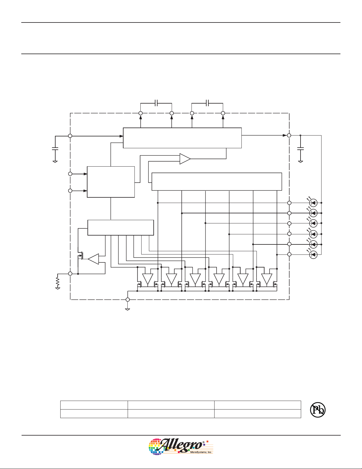
Functional Block Diagram
CIN
1 μF
RSET
VIN
ENM
ENS
ISET
Control, Clock,
and Reference
Current Mirror
+
−
C1+
C1
1 μF
−
C1
Fractional Charge Pump
(1×, 1.5×, and 2×)
−
+
−
+
C2+
+
−
Minimum Select
−
+
C2
1 μF
C2−
VOUT
COUT
1 μF
LED1
LED2
LED3
LED4
LED5
LED6
−
+
−
+
−
+
GND
Ab so lute Max i mum Rat ings
Input or Output Voltage
VIN, VOUT, C1+, C1– , C2+, C2– to GND ..................... –0.3 to 6 V
All other pins ..................................................... –0.3 to V
+ 0.3 V
IN
VOUT Short Circuit to GND ....................................................Continuous
Operating Ambient Temperature, T
Junction Temperature, T
Storage Temperature, T
J(max)
................................................... –55°C to 150°C
S
..................................... –40°C to 85°C
A
.............................................................. 150°C
Use the following complete part number when ordering:
Part Number Packaging* Package Type
A8434EESTR-T 7-in. reel, 1500 pieces/reel ES, 3 × 3 mm MLP-16
*Contact Allegro for additional packing options.
Package Thermal Characteristics
ES Package R
= 68 °C/W
θJA
(vendor data, on 4-layer PCB; unverified)
Additional information is available on the Allegro website.
The device package is lead (Pb) free, with 100% matte tin
leadframe plating.
Allegro MicroSystems, Inc.
115 Northeast Cutoff, Box 15036
Worcester, Massachusetts 01615-0036 (508) 853-5000
www.allegromicro.com
2
A8434
6-Channel High Efficiency Charge Pump
White LED Driver
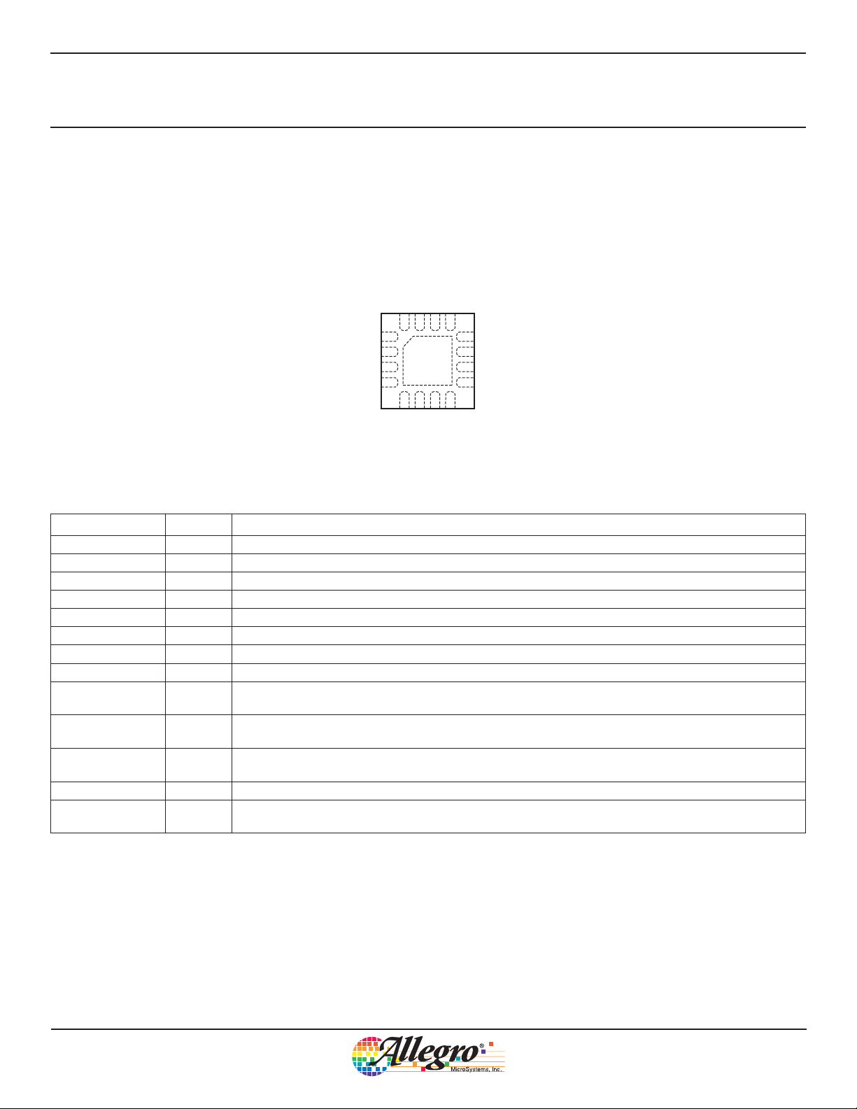
Pin-out Diagram
ES Package
C1+
C2–
VIN
C1–
C2+
VOUT
ISET
ENS
161514
1
2
3
4
567
ENM
(Top View)
EP
LED6
LED5
13
12
11
10
8
LED4
GND
LED1
LED2
9
LED3
Terminal List Table
Name Number Function
C1– 13 Negative terminal of capacitor C1. Connect capacitor C1 between C1+ and C1–.
C1+ 16 Positive terminal of capacitor C1.
C2– 15 Negative terminal of capacitor C2
C2+ 1 Positive terminal of capacitor C2. Connect capacitor C2 between C2+ and C2–.
ENS 4 Enable and dimming control input for sub display WLED group.
ENM 5 Enable and dimming control input for main display WLED group.
EP – Exposed metal pad on bottom side. Connect this to ground plane for better thermal performance.
GND 12 Ground.
ISET 3
LED1, LED2,
LED3, and LED4
8, 9, 10,
and 11
LED5 and LED6 6 and 7
VIN 14 Power supply voltage input.
VOUT 2
Connect RSET resistor to ground to set desired constant current through main and sub WLEDs.
I
LED(max)
= 220 x 0.6 V / R
SET
Current sink for main display WLEDs. If not used, connect to VOUT, but do not leave open. If left
open, the IC works in 2 × mode.
Current sink for sub display WLEDs. If not used, connect to VOUT, but do not leave open. If left open,
the IC works in 2 × mode.
Charge pump output voltage for display backlight and flash/torch LED anodes.
Connect a 1 F capacitor, COUT, between VOUT and GND (see figure 2).
Allegro MicroSystems, Inc.
115 Northeast Cutoff, Box 15036
Worcester, Massachusetts 01615-0036 (508) 853-5000
www.allegromicro.com
3

A8434
6-Channel High Efficiency Charge Pump
White LED Driver
ELECTRICAL CHARACTERISTICS
a
VIN = ENM = ENS = 3.6 V, C1 = C2 = 1 F, CIN = COUT = 1 F, RSET = 6.49 k,
TA = –40°C to +85°C; typical values are at TA = 25°C; unless otherwise noted
Characteristics Symbol Test Conditions Min. Typ. Max. Units
Input Voltage Range V
Undervoltage Lockout Threshold V
UVLO Hysteresis Window V
Quiescent Current I
Soft-start Completion Time t
ISET Bias Voltage V
ISET Leakage in Shutdown V
ISET Current Range I
ISET to LEDx Current Ratio for LED1 through LED6 I
I
Accuracy for LED1 through LED6
LED
LED Current Matching for LED1 through LED4
LED Current Matching for LED5 and LED6
b
c
c
Regulation Voltage at LEDx (1.5× and 2× modes) V
1× mode to 1.5× or 1.5× to 2× mode transition voltage at LEDx V
Transition–Dropout Delta
d
IN
UVLO
UVLOHYS
Q
ss
ISETBIAS
ISETLKG
SET
LEDx/IISET
E
ILEDERR
I
LED14
I
LED56
REG
trans
V
dr
VIN falling 2.25 2.45 2.60 V
Switching in 1.5× or 2.0× mode; TA = 25°C – 6 – mA
ENS = ENM = GND; T
100% setting, I
ENS = ENM = VIN – ±1.6 – %
ENS = GND, ENM = VIN – ±0.5 – %
ENS = VIN, ENM = GND – ±0.5 – %
ENS = ENM = VIN – 250 – mV
V
LEDx
Measured as V
1× mode (VIN – V
Open Loop Output Resistance
e
R
1.5× mode (1.5 × V
OUT
2× mode (2 × V
LED Leakage in Shutdown V
LEDLKG
Oscillator Frequency f
Output Overvoltage Protection (guaranteed by design) V
ENS and ENM Input High Threshold V
ENS and ENM Input Low Threshold V
Input High Current I
Input Low Current I
ENM and ENS Pulse Low Time (figure 5) t
ENM and ENS Pulse High Time (figure 5) t
ENM and ENS Initial Pulse High Time (figure 5) t
Shutdown or Dimming Reset Delay t
INIHI
SHDN
Thermal Shutdown Threshold T
a
Specifications for the range TA = –40°C to 85°C are guaranteed by design.
b
I
accuracy is defined as ( I
LED
c
LED current matching is defined as (I
d
Dropout voltage V
e
The open loop output resistance, R
is defined as LEDx-to-GND voltage at which I
dropout
SET
× 220 – I
LEDx
, for 1.5 × mode is measured when one of the LEDx pins is tied to ground or open (thus its
OUT
LEDAVG
– I
LEDAVG
) / (I
SET
) / I
× 220).
LEDAVG
.
ENS = ENM = GND, VIN = 5.5 V – 0.01 1 A
osc
Open circuit at any LED that is programmed
ovp
to be in the ON state
Input high logic threshold 1.4 – – V
IH
Input low logic threshold – – 0.4 V
IL
VIH=VIN – – 1 A
IH
VIL= GND – – 1 A
IL
LO
HI
First ENM or ENS pulse after shutdown 50 – – s
Falling edge of ENS and/or ENM – 0.5 – ms
20oC hysteresis – 165 –
TSD
LEDx
voltage is always less than 80 mV).
2.7 – 5.5 V
–60–mV
= 25°C – 0.1 2 A
A
– 0.4 – ms
– 0.6 – V
– 0.01 1 A
40 – 140 A
= 60 A – 220 – A/A
SET
falling – 150 – mV
trans
IN
– V
OUT
– V
IN
) / I
– V
OUT
dropout
OUT
OUT
) / I
) / I
OUT
OUT
–40–mV
–1–
– 2.5 –
–5–
– 1 – MHz
– – 6.0 V
0.5 – 250 s
0.5 – – s
o
drops 10% below the value of I
LEDx
when V
= 300 mV.
LEDx
C
Allegro MicroSystems, Inc.
115 Northeast Cutoff, Box 15036
Worcester, Massachusetts 01615-0036 (508) 853-5000
www.allegromicro.com
4

A8434
6-Channel High Efficiency Charge Pump
Performance Characteristics
Tests performed using application circuit shown in figure 2
T
= 25°C, V
A
= 3.6 V (unless otherwise noted)
IN
White LED Driver
Efficiency versus Supply Voltage
VIN falling, Vf = 3.4 V at 20 mA
100.0
95.0
90.0
85.0
80.0
75.0
Eff (%)
70.0
65.0
60.0
55.0
2.7 3.1 3.5 3.9 4.3 4.7 5.1 5.5
Sub
Main
Main + Sub
V
(V)
IN
Logic Level
1.2
1.1
1.0
0.9
(V)
ENx
0.8
V
0.7
0.6
0.5
2.7 3.1 3.5 3.9 4.3 4.7 5.1 5.5
V
HI
VIN(V)
V
LO
Efficiency versus Supply Voltage
VIN falling, Vf = 3.1 V at 10 mA
100.0
95.0
90.0
85.0
Sub
80.0
75.0
Eff (%)
70.0
65.0
60.0
55.0
50.0
2.7 3.1 3.5 3.9 4.3 4.7 5.1 5.5
30
25
20
15
10
per Channel (mA)
LED
I
5
4 6 8 1012141618
R
Main
Main + Sub
V
IN
R
versus LED Current
SET
= 6.65 kΩ
SET
R
=8.87 kΩ
SET
R
SET
(V)
(kΩ)
Dimming on ENM and ENS
Enable Pulses versus Total Current, LED1 through LED6
V
and V
ENM
ENS
C1
I
LED1-6
C2
Symbol Parameter Units/Division
C1 V
C2 I
t time 50 ms
t
LED16
ENM
0.5 V
50 mA
Allegro MicroSystems, Inc.
115 Northeast Cutoff, Box 15036
Worcester, Massachusetts 01615-0036 (508) 853-5000
www.allegromicro.com
5

A8434
6-Channel High Efficiency Charge Pump
Performance Characteristics
Tests performed using application circuit shown in figure 2
T
= 25°C, V
A
Turn ON LED1 through LED6 to 1X Mode
VIN = 4.0 V, I
C2
C1
C4
= 3.6 V (unless otherwise noted)
IN
= 120 mA, VF = 3.4 V
OUT
V
ENM
White LED Driver
and V
ENS
V
OUT
I
OUT
t
Symbol Parameter Units/Division
C2 V
C1 V
C4 I
t time 1 ms
ENM
and V
OUT
OUT
ENS
5.00 V
2.00 V
100 mA
Turn ON LED1 through LED6 to 1.5X Mode
VIN = 3.0 V, I
C2
C1
C4
= 120 mA, VF = 3.4 V
OUT
V
and V
ENM
ENS
V
OUT
I
OUT
t
Symbol Parameter Units/Division
C2 V
C1 V
C4 I
t time 1 ms
ENM
and V
OUT
OUT
ENS
5.00 V
2.00 V
100 mA
Allegro MicroSystems, Inc.
115 Northeast Cutoff, Box 15036
Worcester, Massachusetts 01615-0036 (508) 853-5000
www.allegromicro.com
6

A8434
6-Channel High Efficiency Charge Pump
Performance Characteristics
Tests performed using application circuit shown in figure 2
T
= 25°C, V
A
LED1 through LED6 ON, 2X Mode
VIN = 2.7 V, I
C3
C4
= 3.6 V (unless otherwise noted)
IN
= 120 mA, VF = 3.6 V
OUT
V
OUT(RIPPLE)
I
IN(RIPPLE)
White LED Driver
t
Symbol Parameter Units/Division
C3 V
C4 I
t time 500 ns
OUT(RIPPLE)
IN(RIPPLE)
LED1 through LED6 ON, 1.5X Mode
VIN = 3.6 V, I
C3
C4
Symbol Parameter Units/Division
C3 V
C4 I
t time 500 ns
= 120 mA, VF = 3.6 V
OUT
t
OUT(RIPPLE)
IN(RIPPLE)
20 mV
50 mA
V
OUT(RIPPLE)
I
IN(RIPPLE)
C3
C4
50 mV
50 mA
LED1 through LED4 on, 1.5X Mode
VIN = 3.6 V, I
Symbol Parameter Units/Division
C3 V
C4 I
t time 500 ns
= 80 mA, VF = 3.6 V
OUT
t
OUT(RIPPLE)
IN(RIPPLE)
20 mV
50 mA
V
OUT(RIPPLE)
I
IN(RIPPLE)
Allegro MicroSystems, Inc.
115 Northeast Cutoff, Box 15036
Worcester, Massachusetts 01615-0036 (508) 853-5000
www.allegromicro.com
7

A8434
6-Channel High Efficiency Charge Pump
White LED Driver
Application Information
Setting LED Current
Use the following formula to set the display backlight LED full
current (100%) using RSET on LED1 through LED6. The maxi-
mum current through one LED should not exceed 30 mA:
R
= 0.6 V × 220 / I
where R
is in Ω and I
SET
SET
LEDx
in amperes.
LEDx
Transitions Between 1× and 1.5× or 2× Modes
The A8434 adaptively selects operating mode. When VIN is suf-
ficiently high to maintain V
in 1 × mode unless, as V
IN
the 150 mV threshold. When V
> 150 mV, the A8434 operates
LEDx
drops, the LEDx nodes fall below
falls below 150 mV, the IC
LEDx
enters 1.5× mode.
When the A8434 switches from 1× to 2× mode, it first switches
to 1.5× mode for a typical duration of 1 ms before entering
2× mode.
When operating in 1.5× mode, if V
< VIN, then the IC
OUT
switches back to 1× mode every 130 ms, and then reenters 1.5×
mode again if necessary.
Transitions Between 1.5× and 2× Modes
The transition from 1.5× to 2× mode depends upon dropout
conditions.
When operating in 2× mode, the IC switches back to 1.5× mode
every 130 ms, and then reenters 2× mode again if necessary.
Furthermore, when in 2× mode, whenever a channel disabling
is sensed (that is, whenever ENM is held low for > 0.5 ms with
ENF high, or vice versa), the IC automatically reverts to 1.5×
mode, and then reenters 2× mode again if necessary.
Dimming
Main Display LED1 through LED4 Dimming. The main
display WLEDs (LED1 through LED4) brightness and on/off can
be controlled using digital input at the ENM pin. The ENM pin
accepts one-wire serial pulse input to enable the A8434 and to set
up to 11 dimming levels, from 100% down to 5%.
When ENM is initially pulled up from shutdown, after a softstart, the current for the WLEDs is programmed to 100% of the
setting current, which is determined by the current through the
ISET pin. Each subsequent pulse reduces the backlight LEDs cur-
th
rent by 10%, and the 10
pulse reduces the current by 5%. The
next pulse restores 100% (full) brightness. Figure 5 shows the
timing diagram for ENM control.
95.0
90.0
85.0
80.0
75.0
Eff (%)
70.0
65.0
60.0
55.0
50.0
3.33.43.53.63.73.83.94.04.14.2
Falling
IN
V
VIN (V)
Figure 4. Mode change transition
t
ENM or
ENS
I
ILED
x
SHDN
HI(Init)
0
t
SS
100%
12345 67891011
t
LO
90%
80%
70%
60%
50%
Figure 5. Single-Wire Serial Dimming Control; at pins ENM and ENS.
Rising
IN
V
40%
t
HI
30%
20%
10%
5%
100%
90%
t
SHDN
SHDN or
Dimming
Reset
Allegro MicroSystems, Inc.
115 Northeast Cutoff, Box 15036
Worcester, Massachusetts 01615-0036 (508) 853-5000
www.allegromicro.com
8

A8434
6-Channel High Efficiency Charge Pump
White LED Driver
Sub Display LED5 and LED6 Operation. The sub display
backlight LEDs (LED5 and LED6) brightness and on/off can
be controlled using digital input at the ENS pin. The ENS pin
accepts one-wire serial pulse input to enable the A8434 and to set
up to 11 dimming levels, from 100% down to 5%.
When ENS is initially pulled up from shutdown, after a soft-start,
the current for the backlight LEDs is programmed to 100% of
the setting current, which is determined by the current through
the ISET pin. Each subsequent pulse reduces the LED current
by 10%, and the 10th pulse reduces the current by 5%. The next
pulse restores 100% (full) brightness. Figure 5 shows the timing
diagram for ENS control.
Simultaneous Dimming of All 6 LEDs
For larger displays 6 LEDs can be grouped together. The LEDs
LED1 through LED6 can be dimmed simultaneously by connecting ENM and ENS together and applying serial pulses for
dimming, as shown in figure 1.
Absolute Level Operation Some applications require dimming
to a specific level, regardless of the present level of dimming.
For example, if the IC should dim to 30%, this can be done with
7 steps, as shown in figure 5, irrespective of the dimming level
in effect. This can be achieved by pulling corresponding ENx
pin low for time greater than t
and then applying pulses as
SHDN
shown in figure 5 (7 for 30% dimming). If the pulses are applied
within 2-3 ms, the display flicker is not visible. The procedure is
shown in figure 6.
Shutdown
When the ENM or ENS pin is pulled low for 0.5 ms or longer, the
corresponding display channels are shut off and dimming is reset
to 100% upon the next ENM or ENS going high edge. When both
ENM and ENS are pulled low for 0.5 ms or longer, the A8434
enters the shutdown mode.
Short Circuit Protection
The A8434 is protected against short circuits on the output. When
V
is externally pulled below 1.2 V, the IC enters short circuit
OUT
mode. The A8434 resumes normal operation when the short
circuit is removed.
t > t
SHDN
I
counter resets
SET
t
Symbol Parameter Units/Division
C1 V
C2 V
C3 I
t time 0.5 ms
ENM
OUT
OUT
2.00 V
2.00 V
50 mA
C1
C2
C3
ENx pulled low
100%
Figure 6. Absolute Dimming Level Setting. With ENM pulled low longer the t
pulsing the corresponding ENx pin sets an absolute target level.
Rapid pulse pattern
V
ENM
V
OUT
I
30%
,
SHDN
Allegro MicroSystems, Inc.
115 Northeast Cutoff, Box 15036
Worcester, Massachusetts 01615-0036 (508) 853-5000
www.allegromicro.com
OUT
9

A8434
6-Channel High Efficiency Charge Pump
White LED Driver
Overvoltage Protection
The A8434 is protected up to 4.9 V supply voltage, against
accidental overvoltage caused by an open LED. When any LED
opens, V
will increase till 6 V. Remaining LEDs will continue
OUT
to function normally. Normal operation will be resumed when the
fault is removed.
LED Disconnection
Every LEDx pin has a disable subcircuit, as shown in figure 7.
The A8434 compares the voltage on each LED pin, and if
the voltage on the pin is greater than either V
– 0.4 V or
OUT
VIN – 0.4 V, then the corresponding LED pin is disabled.
If any WLED is not used, connect the corresponding pin to
VOUT. Never leave open any unused WLED pin. LED pins will
sink 20 μA typical when connected to VOUT and the corresponding LED group (main or sub) is enabled.
A8434
V
BATT
CIN
VIN
1×, 1.5×, 2×
Charge Pump
Note: In shutdown mode (ENM = ENS = 0 V for > 0.5 ms), the
total leakage current is < 1μA.
Thermal Shutdown
The IC is internally protected against overtemperature. The
overtemperature limit is set to 165°C nominal. The IC shuts down
when the junction temperature exceeds 165°C and automatically
turns on again when the IC cools.
Component Selection
Ceramic capacitors with X5R or X7R dielectric are recom-
mended for the input capacitor, CIN, the output capacitor, COUT,
and the charge pump capacitors, C1 and C2.
VOUT
COUT
LED Disable Block
One of six blocks
–
V
– 0.4
IN
+
–
V
– 0.4
OUT
+
Current
Sink
LED1
D1
D2
D3
D4
D5
D6
Figure 7. LED disable subcircuit. Subcircuit for one LEDx pin shown. A similar block is
connected to each LEDx pin.
Allegro MicroSystems, Inc.
115 Northeast Cutoff, Box 15036
Worcester, Massachusetts 01615-0036 (508) 853-5000
www.allegromicro.com
10

A8434
6-Channel High Efficiency Charge Pump
White LED Driver
Package ES, 3 × 3 mm16-Pin QFN/MLP
3.15
.124
2.85
.112
16
A
B
C0.08 [.003]
M C A B
.020
.012
1
2
0.50 .020
2
1
0.23 x 0.23
REF
A
16
1.70
.067
NOM
B
.009 x .009
3.15
2.85
1.70
NOM
.124
.112
0.05
0.00
.067
0.20
REF
.002
.000
SEATING
PLANE
0.80
0.70
.008
.031
.028
C
All dimensions reference only, not for tooling use
(reference JEDEC MO-220WEED-4)
Dimensions in millimeters
U.S. Customary dimensions (in.) in brackets, for reference only
Dimensions exclusive of mold flash, gate burrs, and dambar protrusions
Exact case and lead configuration at supplier discretion within limits shown
A
Terminal #1 mark area
Exposed thermal pad (reference only, terminal #1
B
identifier appearance at supplier discretion)
C
Reference land pattern layout (reference IPC7351
QFN50P300X300X80-17W4M); adjust as necessary to
meet application process requirements and PCB layout
tolerances; when mounting on a multilayer PCB, thermal
vias at the exposed thermal pad land can improve thermal
dissipation (reference EIA/JEDEC Standard JESD51-5)
0.30
.012
NOM
0.90
.035
NOM
C
0.20
.008
12X
MIN
4X
0.20
.008
MIN
16
1
1.70
.067
NOM
3.10
.122
NOM
0.50
NOM
1.70
NOM
.020
.067
16X
0.30
.012
16X
0.18
.007
0.10 [.004]
0.05 [.002] M C
0.50
0.30
3.10
.122
NOM
0.20
.008
4X
MIN
Copyright ©2006, Allegro MicroSystems, Inc.
The products described here are manufactured under one or more U.S. patents or U.S. patents pending.
Allegro MicroSystems, Inc. reserves the right to make, from time to time, such de par tures from the detail spec i fi ca tions as may be required to permit improvements in the per for mance, reliability, or manufacturability of its products. Before placing an order, the user is cautioned to verify that the
information being relied upon is current.
Allegro’s products are not to be used in life support devices or systems, if a failure of an Allegro product can reasonably be expected to cause the
failure of that life support device or system, or to affect the safety or effectiveness of that device or system.
The in for ma tion in clud ed herein is believed to be ac cu rate and reliable. How ev er, Allegro MicroSystems, Inc. assumes no re spon si bil i ty for its use;
nor for any in fringe ment of patents or other rights of third parties which may result from its use.
For the latest version of this document, visit our website:
www.allegromicro.com
Allegro MicroSystems, Inc.
115 Northeast Cutoff, Box 15036
Worcester, Massachusetts 01615-0036 (508) 853-5000
www.allegromicro.com
11
 Loading...