

Allegro A8283SLB, A8283SB Datasheet

Data Sheet
PRELIMINARY INFORMATION
(Subject to change without notice)
November 21, 2000
A8283SLB
OSEL
1
OLF
2
VBULK
MIOUT
SENSE
3
4
MI
5
GND
6
GND
7
8
9
LNB
9
LX
VIN
TCAP
Note that the A8283SB (dual in-line package)
and A8283SLB (small-outline IC package) are
electrically identical and share a common
terminal number assignment.
BUCK
10
11
12
REG.
CHARGE
VOLTAGE
ABSOLUTE MAXIMUM RATINGS
Supply Voltage, VIN.......................... 47 V
Output Current, IO.... Internally Limited
Logic Input Voltage Range,
VI................................... -0.5 V to +7 V
Bypass Switch Current,
ISW........................ Internally Limited
Flag Output Voltage, V
Operating Temperature Range,
TA............................... -20°C to +85°C
Storage Temperature Range,
TS............................. -40°C to +150°C
.................. 7 V
OLF
EXTM
24
VINT
23
PUMPX
22
VPUMP
21
PUMP
CPUMP
20
GND
19
18
GND
ENT
17
EN
16
VSEL0
15
VSEL1
14
CONTROL
LLC
13
Dwg. PP-072A
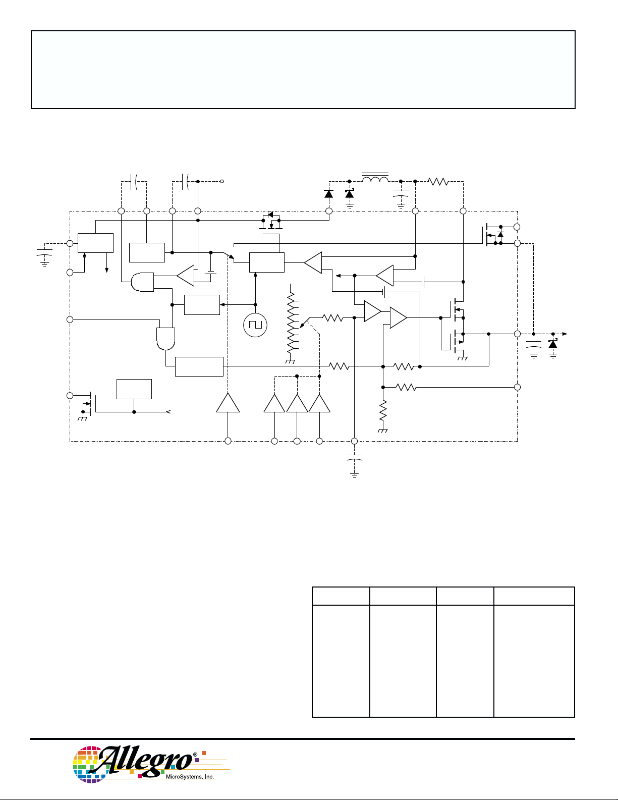
8283
LNB SUPPLY AND
CONTROL-VOLTAGE REGULATOR
Intended for analog and digital satellite receivers, the low-noise block
converter regulator (LNBR) is a monolithic linear and switching voltage
regulator designed to provide power and interface signals to the LNB down
converter via the coaxial cable. If the device is in stand-by mode (EN terminal
LOW), the regulator output is disabled, allowing the antenna downconverters to
be supplied or controlled by other satellite receivers sharing the same coaxial
cable. Similar two-output LNB supply and control voltage regulators are the
A8284SB/SLB.
For slave operation in single-dish dual-receiver systems, the bypass
function is implemented by an electronic switch between the master input
terminal (MI) and the LNB terminal, leaving all LNB power and control
functions to the master receiver. This electronic switch is closed if the device
is powered, EN is HIGH, and OSEL is LOW.
The regulator outputs are set to 12, 13, 18, or 20 V by the VSEL terminals.
Additionally, it is possible to increase the selected voltage by 1 V to compensate for the voltage drop in the coaxial cable (LLC terminal HIGH). The
LNBR combines a tracking switching regulator and low-noise linear regulator.
Logic inputs (VSEL0, VSEL1, and LLC) select the desired output voltage. A
tracking current-mode buck converter provides the linear regulator with an
input voltage that is set to the output voltage plus typically 0.8 V. This maintains constant voltage drop across the linear regulator while permitting adequate voltage range for tone injection.
The device is supplied in a 24-pin plastic DIP with batwing tabs
(A8283SB), or a 24-lead SOIC power-tab package (A8283SLB). In both cases,
the power tab is at ground potential and needs no electrical isolation.
FEATURES
■ Short-Circuit Protected Bypass Function for Slave Operation
■ LNB Selection and Stand-By Function
■ Built-In Tone Oscillator Factory Trimmed to 22 kHz, Facilitates
DiSEqC™ (a trademark of EUTELSAT) Encoding
■ Full Modulation With No Load
■ Tracking Switch-Mode Power Converter for Lowest Dissipation
■ Externally Adjustable Short-Circuit Protection
■ LNB Short-Circuit Protection and Diagnostics
■ Auxiliary Modulation Input
■ Cable Length Compensation
■ Internal Over-Temperature Protection
This device incorporates features that have patents pending.
Always order by complete part number, e.g., A8283SLB .
27448
8283
LNB SUPPLY AND
CONTROL-VOLTAGE REGULATOR
FUNCTIONAL BLOCK DIAGRAM
VINT
ENT
OLF
VBULK
150 mV
RS
SENSE
MI
MIOUT
LNB
EXTM
Dwg. FP-051-1
47 V
MAX
VPUMP
CHARGE
TSD
PUMP
CPUMP
176 kHz
OVERCURRENT
PUMPX
VOLTAGE
REG.
EN
5 V
VIN
BOOST
VOLTAGE
–
+
÷2
÷8
&
WAVESHAPING
7 V
0
1
352 kHz
22 kHz TONE
OSEL
BUCK
CONV.
VREF
VSEL0
VSEL1
LX
–
OVER-
+
CURRENT
800 mV
TCAP
–
+
25 kΩ
LLC
–
+
1 kΩ
+
+
–
5 kΩ
5 kΩ
Output Voltage Select Table
VSEL0 VSEL1 LLC V
LLL13 V
L L H 14 V
LHL18 V
L H H 19 V
H L L 12 V
H L H 13 V
H H L 20 V
HHH21 V
2
115 Northeast Cutoff, Box 15036
Worcester, Massachusetts 01615-0036 (508) 853-5000
Copyright © 2000, Allegro MicroSystems, Inc.
LNB(typ)

8283
LNB SUPPLY AND
CONTROL-VOLTAGE REGULATOR
ELECTRICAL CHARACTERISTICS at TA = 25°C, ENT = L, EN = H, OSEL = H, LLC = L, V
I
= 50 mA (unless otherwise noted).
O
= 24 V,
IN
Limits
Characteristic Symbol Test Conditions Min. Typ. Max. Units
Supply Voltage V
Output Voltage V
Line Regulation ∆V
IN
O
O
IO = 600 mA, VSEL0 = L, VSEL1 = L, LLC = L
IO = 600 mA, VSEL0 = L, VSEL1 = L, LLC = L
IO = 600 mA, VSEL0 = L, VSEL1 = L, LLC = H
IO = 600 mA, VSEL0 = L, VSEL1 = H, LLC = L
IO = 600 mA, VSEL0 = L, VSEL1 = H, LLC = H
IO = 600 mA, VSEL0 = H, VSEL1 = L, LLC = L
IO = 600 mA, VSEL0 = H, VSEL1 = L, LLC = H
IO = 600 mA, VSEL0 = H, VSEL1 = H, LLC = L
IO = 600 mA, VSEL0 = H, VSEL1 = H, LLC = H
—
3.3 + ∆V
BUCK
47 V
12.5 13 13.5 V
13.4 14 14.6 V
17.3 18 18.7 V
18.2 19 19.8 V
11.5 12 12.5 V
12.5 13 13.5 V
19.2 20 20.8 V
20.2 21 21.8 V
VO = 13 V, VI = 16 to 40 V — 4.0 40 mV
VO = 18 V, VI = 21 to 40 V — 4.0 40 mV
Load Regulation ∆V
Current-Limiting Threshold V
Tone Frequency f
Tone Amplitude V
OM(th)
tone
tone(PP)
Tone Duty Cycle dc
Tone Rise or Fall Time tr, t
External Modulation Gain G
External Modulation V
mod
mod(PP)
O
tone
f
VO = 13 or 18 V, IO = 50 to 600 mA — 80 180 mV
125 135 145 mV
ENT = H 20 22 24 kHz
ENT = H 550 680 800 mV
ENT = H 40 50 60 %
ENT = H 5.0 10 15 µs
∆VO/∆V
, f = 10 Hz to 40 kHz — 5.0 — V/V
mod
AC coupling — — 160 mV
Input Voltage
External Modulation Z
Impedance
www.allegromicro.com
mod
f = 10 Hz to 40 kHz — 5.0 — kΩ
continued next page ...
3
 Loading...