

Allegro A8188SLT-33, A8188SLT-32, A8188SLT-31, A8188SLT-30, A8188SLT-29 Datasheet
...
DISCONTINUED PRODUCT
— FOR REFERENCE ONLY
8188
Designed specifically to meet the requirement for extended operation of battery-powered equipment such as cordless and cellular telephones, the A8188S— voltage regulators offer the reduced dropout
voltage and quiescent current essential for maximum battery life.
Applicable also to palmtop computers and personal data assistants,
these devices deliver a regulated output at up to 250 mA (transient),
which is limited only by package power dissipation. Regulated output
voltages between 2.5 V and 3.3 V are trimmed at wafer probe.
A PMOS pass element provides a typical dropout voltage of only
90 mV at 60 mA of load current. The low dropout voltage permits
deeper battery discharge before output regulation is lost. Quiescent
current does not increase significantly as the dropout voltage is approached, an ideal feature in standby/resume power systems where data
integrity is crucial. Regulator accuracy and excellent temperature
characteristics are provided by a bandgap reference. The A8188SL-xx
includes ENABLE inputs to give the designer complete control over
power up, standby, or power down.
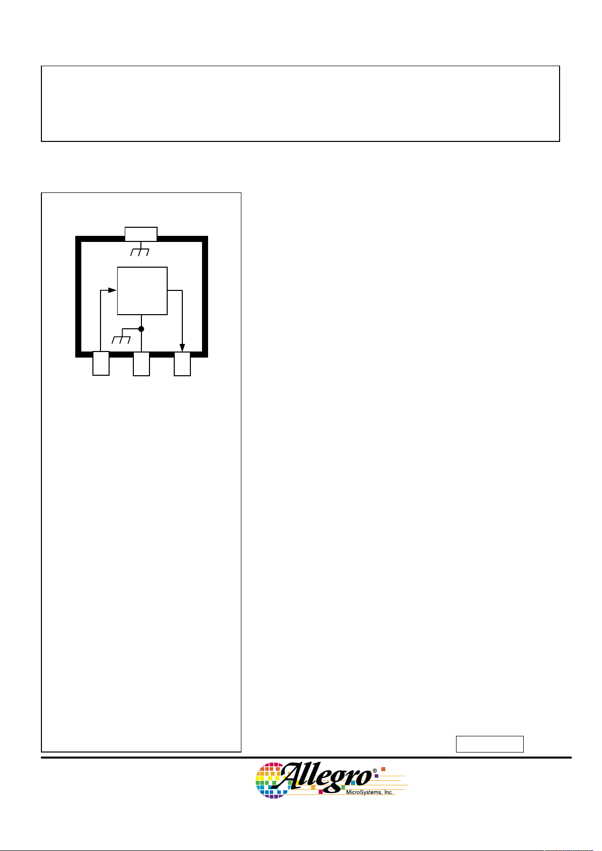
These devices are supplied, without the ENABLE function, in a
standard 3-lead SOT-89/TO-243AA small-outline plastic transistor
package (suffix ‘LT’). Dual regulators (A8188SL-xx) are provided in
an 8-lead SOIC package. All devices are rated for operation over a
temperature range of -20°C to +85°C.
FEATURES AND BENEFITS
■ High Efficiency Provides Extended Battery Life
■ 90 mV Typical Dropout Voltage at I
O
= 60 mA
■ 55 µA Typical Quiescent Current
Less Than 1 µA “Sleep” Current
■ 250 mA Peak Output Current
■ Improved PSRR and Transient Performance
■ Internal Thermal Protection
APPLICATIONS
■ Cordless and Cellular Telephones
■ Personal Data Assistants
■ Personal Communicators
■ Palmtop Computers
LOW-DROPOUT REGULATORS
— HIGH EFFICIENCY
Always order by complete part number, e.g., A8188SLT-30 .
A8188SLT-xx
PRELIMINARY INFORMATION
(subject to change without notice)
July 13, 1999
Dwg. PS-022-2
VR
2
31
GND
OUT
IN
where “-xx” is the required output voltage in tenths
Data Sheet
27468.8
ABSOLUTE MAXIMUM RATINGS
Input Voltage, V
I
. . . . . . . . . . . . . . 10 V
Peak Output Current,
IOM. . . . . . . . . . . . . . . . . . 250 mA*
Enable Input Voltage, VE. . . . . . . . . V
I
Operating Temperature Range,
T
A
. . . . . . . . . . . . . -20°C to +85°C
Junction Temperature, T
J
. . . . +150°C
†
Storage Temperature Range,
T
S
. . . . . . . . . . . . -40°C to +150°C
* Output current rating is limited by input
voltage, duty cycle, and ambient temperature. Under any set of conditions, do not
exceed a junction temperature of +150°C.
See following pages.
† Fault conditions that produce excessive
junction temperature will activate device
thermal shutdown circuitry. These conditions can be tolerated but should be
avoided.
8188
LOW-DROPOUT
REGULATORS
115 Northeast Cutoff, Box 15036
Worcester, Massachusetts 01615-0036 (508) 853-5000
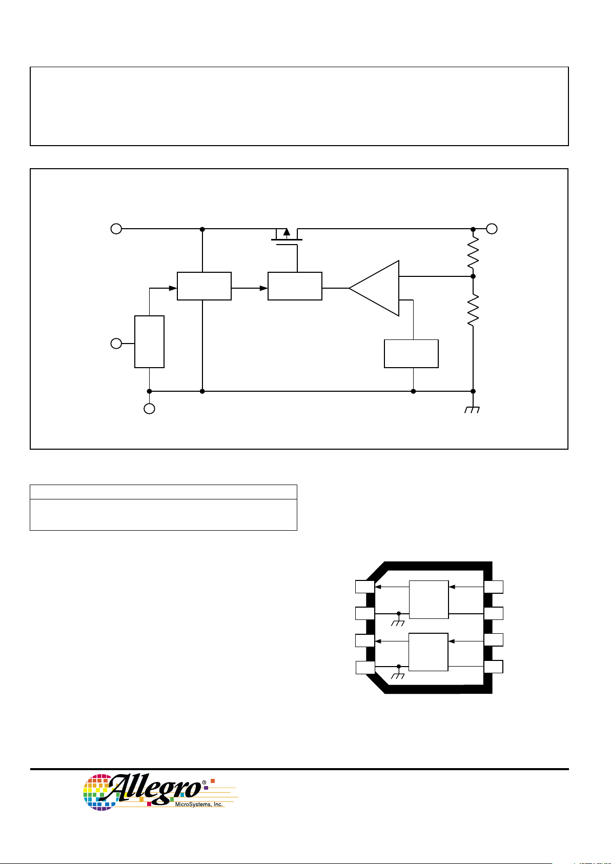
FUNCTIONAL BLOCK DIAGRAM
(1/2 of A8188SL-xx shown)
Dwg. FS-012-8
BIAS
DRIVE
ENABLE
BANDGAP
REF.
ERROR
AMP
IN
ENABLE
OUT
8 1
7
2
GND
A8188SL-xx
1
2
3
Dwg. PS-023
6
7
8
GND
GND
OUT
OUT
ENABLE
IN
IN
ENABLE
1
1
2
2
VR
4
5
VR
1
1
2
2
Always order by complete part number:
Part Number Package R
θJA
A8188SL-xx 8-Lead SOIC 108°C/W
A8188SLT-xx 3-Lead SOT-89/TO-243AA 258°C/W
where “-xx” is the required output voltage (V
O(nom)
) in tenths
(25 through 33), e.g., -30 = 3.0 volts.
Copyright © 1999, 2000 Allegro MicroSystems, Inc.
NOTE — There is an indeterminate resistance between terminals
2 and 4. For proper operation, terminals 2 and 4 must be
externally connected together.
8188
LOW-DROPOUT
REGULATORS
www.allegromicro.com
A8188SL-xx Maximum Allowable Total Average Output Current* with device mounted on 2.24" x
2.24" (56.9 mm x 56.9 mm) solder-coated copper-clad board in still air.
Allowable Total Average (10 ms) Output Current in Milliamperes with TJ = 150°C, Duty Cycle = 100%†
VI - V
O
T
A
1.0 1.5 2.0 2.5 3.0 4.0 5 .0 6.0 7.0*
25°C 500 500 500 460 385 285 230 190 165
50°C 500 500 460 370 305 230 185 150 130
70°C 500 490 370 295 245 185 145 120 105
85°C 500 400 300 240 200 150 120 100 85
* Absolute maximum peak output current rating for either output is 250 mA; absolute maximum input voltage is 10 V.
†I
O
= (TJ – TA)/([VI – VO] R
θJA
x dc) = (150 – TA)/([VI – VO] x 108 x 1.00)
Output current rating can be increased (to 250 mA maximum per output) by additional heat sinking or reducing the duty
cycle. Conditions that produce excessive junction temperature will activate device thermal shutdown circuitry. These
conditions can be tolerated but should be avoided.
A8188SLT-xx Maximum Allowable Output Current with device mounted on 2.24" x 2.24" (56.9 mm
x 56.9 mm) solder-coated copper-clad board in still air.
Allowable Average (10 ms) Output Current in Milliamperes with TJ = 150°C, Duty Cycle = 100%†
VI - V
O
T
A
1.0 1.5 2.0 2.5 3.0 4.0 5.0 6.0 7.0*
25°C 250 250 240 190 160 120 95 80 65
50°C 250 250 190 155 125 95 75 65 55
70°C 250 205 155 120 100 75 60 50 40
85°C 250 165 125 100 80 60 50 40 35
* Absolute maximum input voltage is 10 V.
†I
O
= (TJ – TA)/([VI – VO] R
θJA
x dc) = (150 – TA)/([VI – VO] x 258 x 1.00)
Output current rating can be increased (to 250 mA maximum) by additional heat sinking or reducing the duty cycle.
Conditions that produce excessive junction temperature will activate device thermal shutdown circuitry. These conditions
can be tolerated but should be avoided.
8188
LOW-DROPOUT
REGULATORS
115 Northeast Cutoff, Box 15036
Worcester, Massachusetts 01615-0036 (508) 853-5000
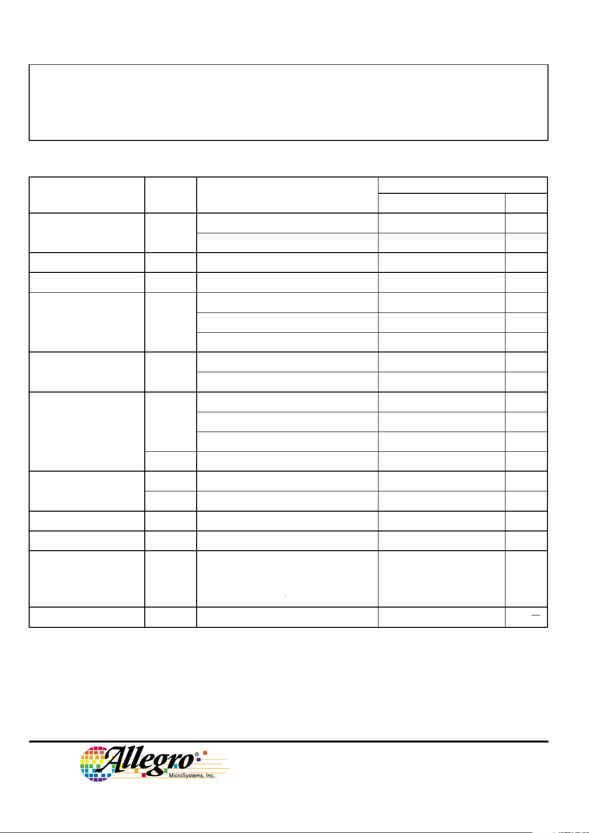
ELECTRICAL CHARACTERISTICS at T
A
= +25°C (unless otherwise noted).
Limits
Characteristic Symbol Test Conditions Min. Typ. Max. Units
Output Voltage V
O
4 V ≤ VI ≤ 8 V, 10 µA ≤ IO ≤ 100 mA* -0.05 0.00 +0.05 V
(reference specified V
O(nom)
)
V
I
= V
O(nom)
, IO = 60 mA -0.30 — — V
Output Volt. Temp. Coeff. a
VO
VI = 6 V, IO = 10 mA, TJ ≤ 125°C — -0.30 — mV/°C
Line Regulation ∆V
O(∆VI)
4 V ≤ VI ≤ 8 V, IO = 1 mA — — 10 mV
Load Regulation ∆V
O(∆IO)
1 mA ≤ IO ≤ 100 mA*, VI = 8 V — — 40 mV
1 mA ≤ IO ≤ 100 mA*, VI = 6 V — — 40 mV
1 mA ≤ IO ≤ 100 mA*, VI = 4 V — — 40 mV
Dropout Voltage VImin – VOIO = 60 mA — 90 150 mV
IO = 125 mA* — 190 300 mV
Quiescent Current I
Q
VI = 8 V, IO ≤ 1 mA, VE ≥ 2.0 V — 55 70 µA
(GND terminal current)
V
I
= 8 V, IO ≤ 100 mA*, VE ≥ 2.0 V — 70 85 µA
VI = V
O(nom)
, IO = 60 mA — 200 — µA
I
Q(off)
4 V ≤ VI ≤ 8 V, VE ≤ 0.8 V — — 1.0 µA
ENABLE Input Voltage V
EH
4 V ≤ VI ≤ 8 V, Output ON 2.0 — — V
V
EL
4 V ≤ VI ≤ 8 V, Output OFF — — 0.8 V
ENABLE Input Current I
E
VE = VI = 8 V — — ±1.0 µA
Thermal Shutdown Temp. T
J
150 — — °C
Rejection Ratio PSRR
VI = V
O(nom)
+ 1.5 V, Vi = 100 mV, IO = 10 mA:
f = 1 kHz — 60 — dB
f = 10 kHz – 50 — dB
Noise e
n
10 Hz ≤ f ≤ 100 kHz, IO = 10 mA, CO = 10 µF — 2.0 — µV/√Hz
Typical values are at TA = +25°C and are given for circuit design information only.
* Pulse test (≤20 ms). See previous page for duty cycle limitations.
 Loading...