

Allegro A6B595KLW, A6B595KA Datasheet
6B595
Data Sheet
26185.122
ADVANCE INFORMATION
(Subject to change without notice)
January 24, 2000
NO
CONNECTION
LOGIC
SUPPLY
SERIAL
DATA IN
OUT
OUT
OUT
OUT
REGISTER
CLEAR
OUTPUT
ENABLE
GROUND
1
2
V
DD
3
4
0
5
1
6
2
7
3
8
9
10
CLR
OE
LATCHES
REGISTER
NCNC
LATCHES
REGISTER
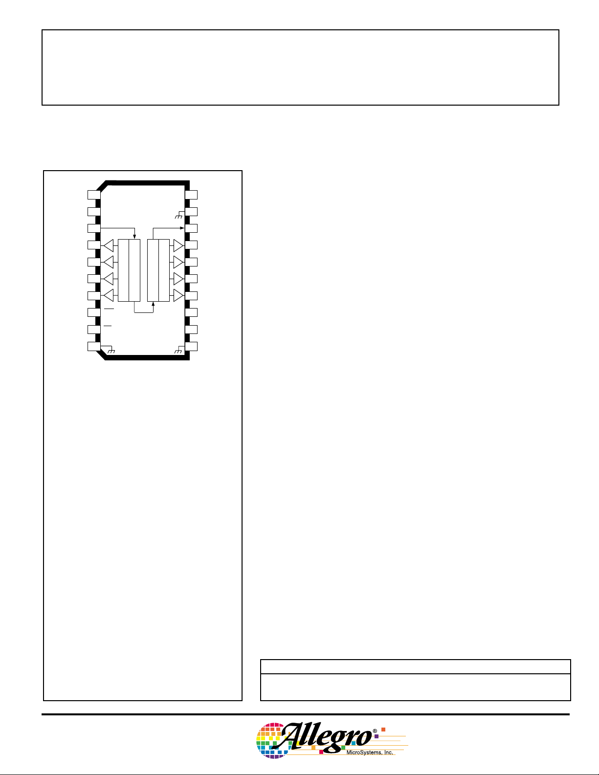
Note that the A6B595KA (DIP) and the
A6B595KLW (SOIC) are electrically identical and
share a common terminal number assignment.
ABSOLUTE MAXIMUM RATINGS
at T
= 25°C
A
Output Voltage, VO............................... 50 V
Output Drain Current,
Continuous, IO.......................... 150 mA*
Peak, IOM................................... 500 mA†
Single-Pulse Avalanche Energy,
EAS................................................. 30 mJ
Logic Supply Voltage, VDD.................. 7.0 V
Input Voltage Range,
VI................................... -0.3 V to +7.0 V
Package Power Dissipation,
PD........................................... See Graph
Operating Temperature Range,
TA................................. -40°C to +125°C
Storage Temperature Range,
TS................................. -55°C to +150°C
* Each output, all outputs on.
† Pulse duration ≤ 100 µs, duty cycle ≤ 2%.
Caution: These CMOS devices have input static
protection (Class 3) but are still susceptible to
damage if exposed to extremely high static
electrical charges.
ST
20
19
18
17
16
15
14
13
12
11
NO
CONNECTION
GROUND
SERIAL
DATA OUT
OUT
7
OUT
6
OUT
5
OUT
4
CLOCKCLK
STROBE
GROUND
Dwg. PP-029-12
8-BIT SERIAL-INPUT,
DMOS POWER DRIVER
The A6B595KA and A6B595KLW combine an 8-bit CMOS shift
register and accompanying data latches, control circuitry, and DMOS
power driver outputs. Power driver applications include relays, solenoids, and other medium-current or high-voltage peripheral power
loads.
The serial-data input, CMOS shift register and latches allow direct
interfacing with microprocessor-based systems. Serial-data input rates
are over 5 MHz. Use with TTL may require appropriate pull-up
resistors to ensure an input logic high.
A CMOS serial-data output enables cascade connections in applications requiring additional drive lines. Similar devices with reduced
r
are available as the A6595KA and A6595KLW.
DS(on)
The A6B595 DMOS open-drain outputs are capable of sinking up
to 500 mA. All of the output drivers are disabled (the DMOS sink
drivers turned off) by the OUTPUT ENABLE input high.
The A6B595KA is furnished in a 20-pin dual in-line plastic
package. The A6B595KLW is furnished in a wide-body, small-outline
plastic package (SOIC) with gull-wing leads. Copper lead frames,
reduced supply current requirements, and low on-state resistance allow
both devices to sink 150 mA from all outputs continuously, to ambient
temperatures over 85°C.
FEATURES
■ 50 V Minimum Output Clamp Voltage
■ 150 mA Output Current (all outputs simultaneously)
■ 5 Ω Typical
■ Low Power Consumption
■ Replacements for TPIC6B595N and TPIC6B595DW
Always order by complete part number:
Part Number Package R
A6B595KA 20-pin DIP 55°C/W 25°C/W
A6B595KLW 20-lead SOIC 70°C/W 17°C/W
r
DS(on)
θJA
R
θJC
6B595
g
8-BIT SERIAL-INPUT,
DMOS POWER DRIVER
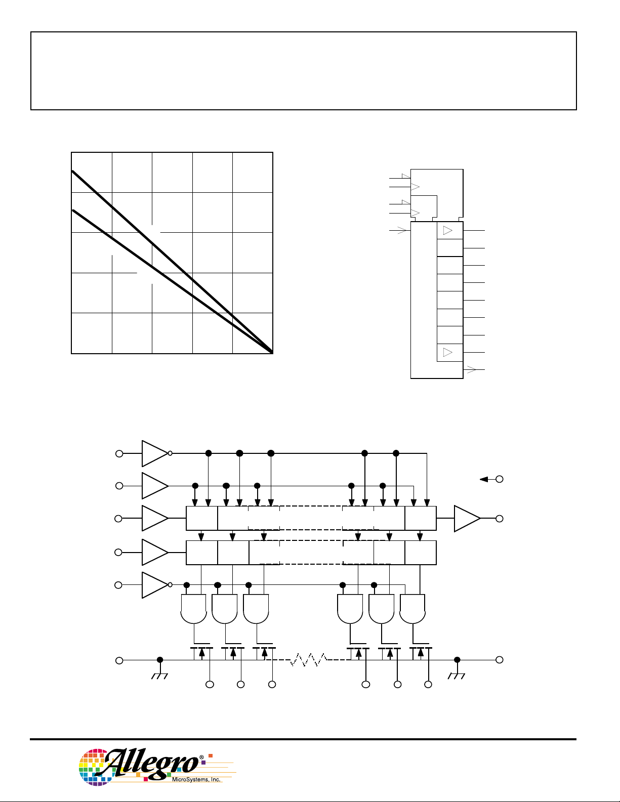
2.5
2.0
SUFFIX 'A', R = 55
1.5
1.0
SUFFIX 'LW
θ
J
A
', R = 70
θ
J
A
°C/W
°C/W
0.5
0
25
ALLOWABLE PACKAGE POWER DISSIPATION IN WATTS
50 75 100 125 150
AMBIENT TEMPERATURE IN °C
Dwg. GS-004A
FUNCTIONAL BLOCK DIAGRAM
LOGIC SYMBOL
9
12
8
13
3
G3
R
1D
C2
SRG8
C1
2
2
Dw
4
5
6
7
14
15
16
17
18
. FP-043
REGISTER
CLEAR
(ACTIVE LOW)
CLOCK
SERIAL
DATA IN
STROBE
OUTPUT
ENABLE
(ACTIVE LOW)
GROUND
V
SERIAL-PARALLEL SHIFT REGISTER
D-TYPE LATCHES
OUT
0
OUT
N
Grounds (terminals 10, 11, and 19) must be connected together externally.
DD
LOGIC
SUPPLY
SERIAL
DATA OUT
GROUND
Dwg. FP-013-4
115 Northeast Cutoff, Box 15036
Worcester, Massachusetts 01615-0036 (508) 853-5000
Copyright © 1999, Allegro MicroSystems, Inc.
IN
Dwg. EP-010-16
6B595
8-BIT SERIAL-INPUT,
DMOS POWER DRIVER
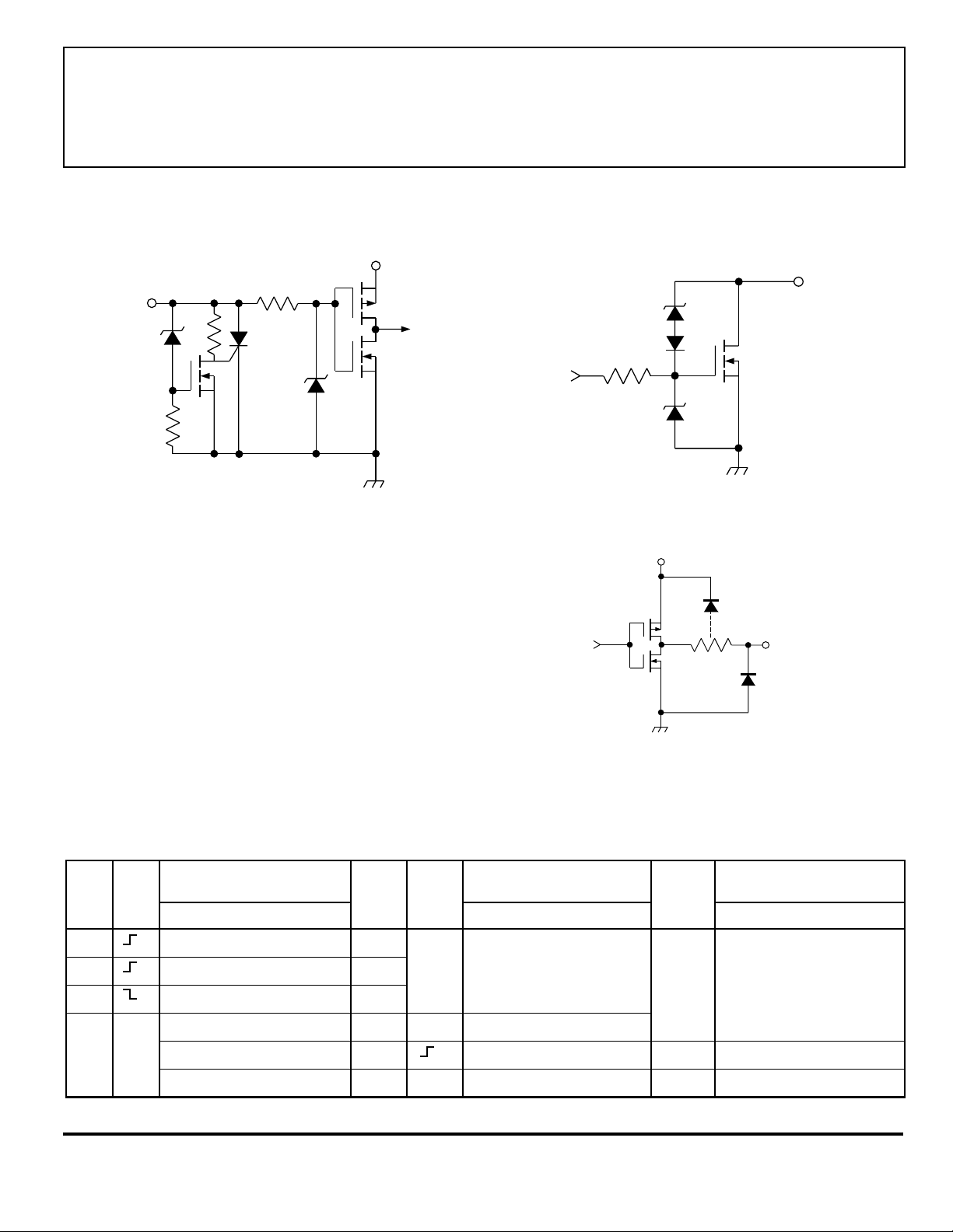
V
DD
OUT
Dwg. EP-063
LOGIC INPUTS
DMOS POWER DRIVER OUTPUT
V
DD
RECOMMENDED OPERATING CONDITIONS
over operating temperature range
Logic Supply Voltage Range, VDD............... 4.5 V to 5.5 V
High-Level Input Voltage, V
Low-level input voltage, V
............................ ≥ 0.85V
IH
................................. ≤0.15V
IL
DD
DD
SERIAL DATA OUT
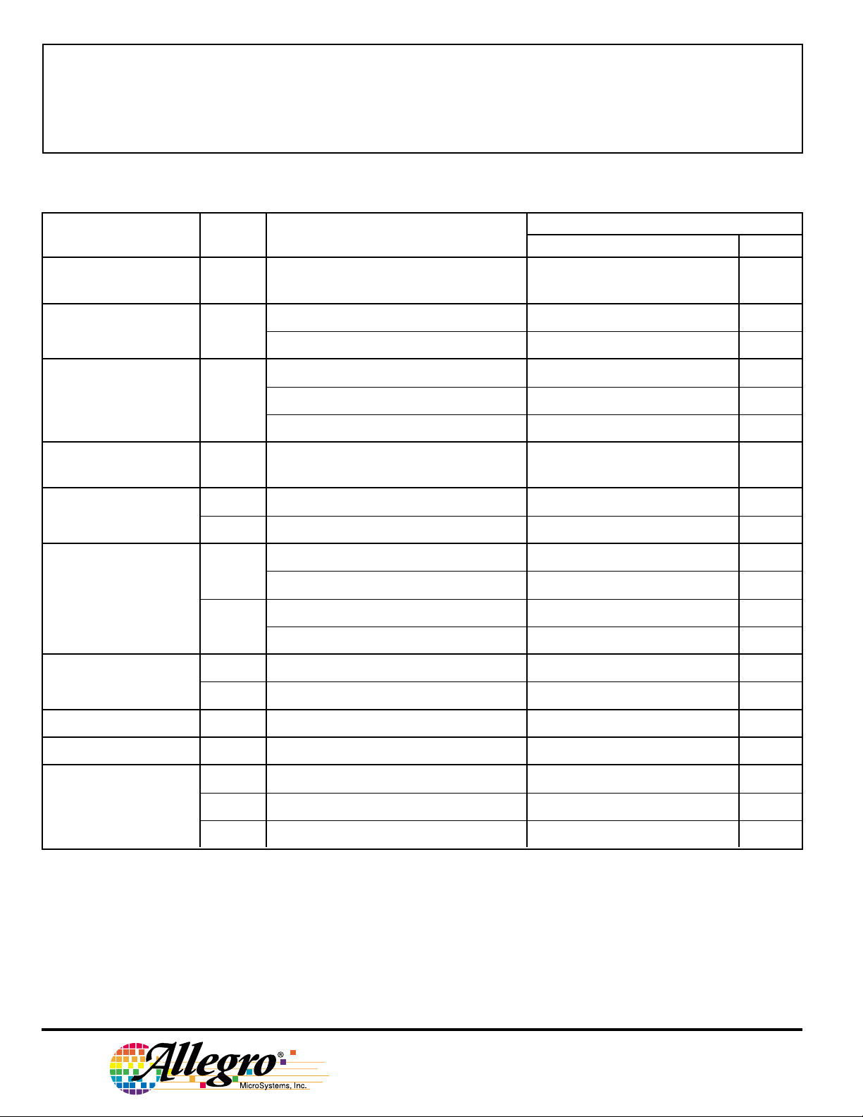
TRUTH TABLE
Shift Register Contents Serial Latch Contents Output Contents
Data Clock Data Output
Input Input I0I1I
HHR
LLR
XR
0R1
0R1
0R1R2
XXX … XX X — R0R1R2…R6R
P0P1P2…P6P
... I6I7Output Strobe I0I1I2... I6I7Enable I0I1I2…I6I
2
…R5R
…R5R
…R6R
R
6
6
R
6
6
R
7
7
7
P
7
7
P0P1P2…P6P
LP0P1P2…P6P
7
XXX … XX H HHH… HH
OUT
Dwg. EP-063-1
7
7
L = Low Logic Level H = High Logic Level X = Irrelevant P = Present State R = Previous State
www.allegromicro.com
6B595
8-BIT SERIAL-INPUT,
DMOS POWER DRIVER
ELECTRICAL CHARACTERISTICS at T
= +25°C, V
A
= 5 V, tir = t
DD
≤ 10 ns (unless otherwise
if
specified).
Limits
Characteristic Symbol Test Conditions Min. Typ. Max. Units
Output Breakdown V
(BR)DSXIO
Voltage
Off-State Output I
Current
Static Drain-Source r
DS(on)
On-State Resistance
Nominal Output I
Current
Logic Input Current I
SERIAL-DATA V
Output Voltage
DSX
ON
IH
I
IL
OH
= 1 mA 50 — — V
VO = 40 V, V
VO = 40 V, VDD = 5.5 V, T
IO = 100 mA, V
IO = 100 mA, VDD = 4.5 V, T
IO = 350 mA, V
V
= 0.5 V, T
DS(on)
VI = V
DD
VI = 0, V
I
= -20 µA, V
OH
= 5.5 V — 0.1 5.0 µA
DD
= 125°C — 0.15 8.0 µA
A
= 4.5 V — 4.2 5.7 Ω
DD
= 125°C— 6.8 9.5 Ω
A
= 4.5 V (see note) — 5.5 8.0 Ω
DD
= 85°C—90—mA
A
= 5.5 V — — 1.0 µA
= 5.5 V — — -1.0 µA
DD
= 4.5 V 4.4 4.49 — V
DD
IOH = -4 mA, VDD = 4.5 V 4.0 4.2 — V
V
OL
I
= 20 µA, V
OL
= 4.5 V — 0.005 0.1 V
DD
IOL = 4 mA, VDD = 4.5 V — 0.3 0.5 V
Prop. Delay Time t
t
Output Rise Time t
Output Fall Time t
Supply Current I
DD(OFF)
I
DD(ON)
I
DD(fclk)
PLH
PHL
r
f
IO = 100 mA, CL = 30 pF — 150 — ns
IO = 100 mA, CL = 30 pF — 90 — ns
IO = 100 mA, CL = 30 pF — 200 — ns
IO = 100 mA, CL = 30 pF — 200 — ns
V
= 5.5 V, Outputs OFF — 20 100 µA
DD
V
= 5.5 V, Outputs ON — 150 300 µA
DD
f
= 5 MHz, CL = 30 pF, Outputs OFF — 0.4 5.0 mA
clk
Typical Data is at VDD = 5 V and is for design information only.
NOTE — Pulse test, duration ≤100 µs, duty cycle ≤2%.
115 Northeast Cutoff, Box 15036
Worcester, Massachusetts 01615-0036 (508) 853-5000
 Loading...