

Allegro A6B259KLW, A6B259KA Datasheet
6B259
Data Sheet
26186.122
ADVANCE INFORMATION
(Subject to change without notice)
January 24, 2000
NO (INTERNAL)
CONNECTION
S (LSB)
GROUND
GROUND
Note that the A6B259KA (DIP) and the A6B259KLW
(SOIC) are electrically identical and share a common
terminal number assignment.
LOGIC
SUPPLY
0
OUT
OUT
OUT
OUT
LOGIC
POWER
1
NC
2
V
DD
3
4
0
5
1
6
2
7
3
8
S
1
9
10
LATCHES
DECODER LOGIC
LATCHES
ABSOLUTE MAXIMUM RATINGS
at T
= 25°C
Output Voltage, VO............................... 50 V
Output Drain Current,
Continuous, IO.......................... 150 mA*
Peak, IOM................................... 500 mA†
Single-Pulse Avalanche Energy,
EAS................................................. 30 mJ
Logic Supply Voltage, VDD.................. 7.0 V
Input Voltage Range,
VI................................... -0.3 V to +7.0 V
Package Power Dissipation,
PD........................................... See Graph
Operating Temperature Range,
TA................................. -40°C to +125°C
Storage Temperature Range,
TS................................. -55°C to +150°C
* Each output, all outputs on.
† Pulse duration ≤ 100 µs, duty cycle ≤ 2%.
Caution: These CMOS devices have input static
protection (Class 3) but are still susceptible to damage if
exposed to extremely high static electrical charges.
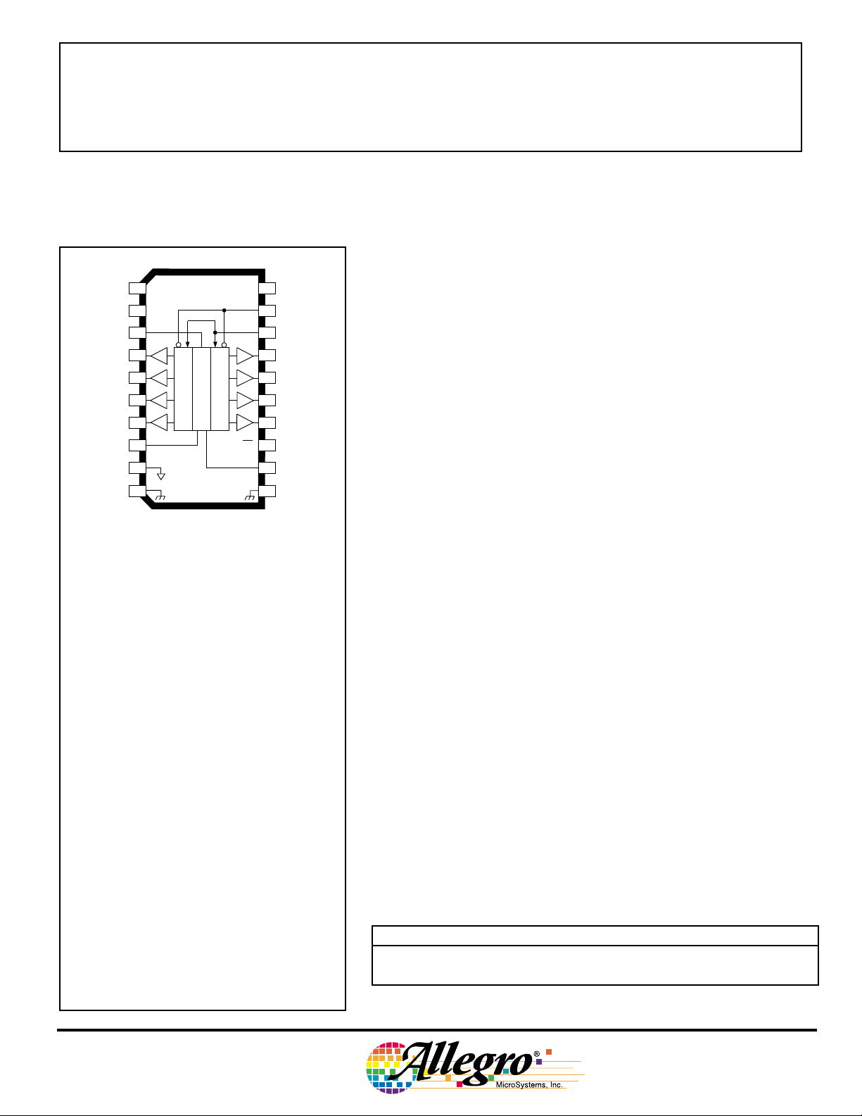
A
NC
EN
NO (INTERNAL)
CONNECTION
19
CLEAR
1820DATA
OUT
17
OUT
16
OUT
15
14
OUT
ENABLE
13
12
S (MSB)
2
POWER
11
GROUND
Dwg. PP-050-1
7
6
5
4
8-BIT ADDRESSABLE
DMOS POWER DRIVER
The A6B259KA and A6B259KLW combine a 3-to-8 line CMOS
decoder and accompanying data latches, control circuitry, and DMOS
outputs in a multi-functional power driver capable of storing single-line
data in the addressable latches or use as a decoder or demuliplexer.
Driver applications include relays, solenoids, and other mediumcurrent or high-voltage peripheral power loads.
The CMOS inputs and latches allow direct interfacing with microprocessor-based systems. Use with TTL may require appropriate pullup resistors to ensure an input logic high. Four modes of operation are
selectable with the CLEAR and ENABLE inputs.
The A6B259KA/KLW DMOS open-drain outputs are capable of
sinking up to 500 mA. Similar devices with reduced r
able as the A6259KA/KLW.
The A6B259KA is furnished in a 20-pin dual in-line plastic
package. The A6B259KLW is furnished in a 20-lead wide-body,
small-outline plastic package (SOIC) with gull-wing leads for surfacemount applications. Copper lead frames, reduced supply current
requirements, and low on-state resistance allow either device to sink
150 mA from all outputs continuously, to ambient temperatures greater
than 85°C.
FEATURES
■ 50 V Minimum Output Clamp Voltage
■ 150 mA Output Current (all outputs simultaneously)
■ 5 Ω Typical
■ Low Power Consumption
■ Replacements for TPIC6B259N and TPIC6B259DW
Always order by complete part number:
Part Number Package R
A6B259KA 20-pin DIP 55°C/W 25°C/W
A6B259KLW 20-lead SOIC 70°C/W 17°C/W
r
DS(on)
θJA
DS(on)
are avail-
R
θJC
6B259
g
8-BIT ADDRESSABLE
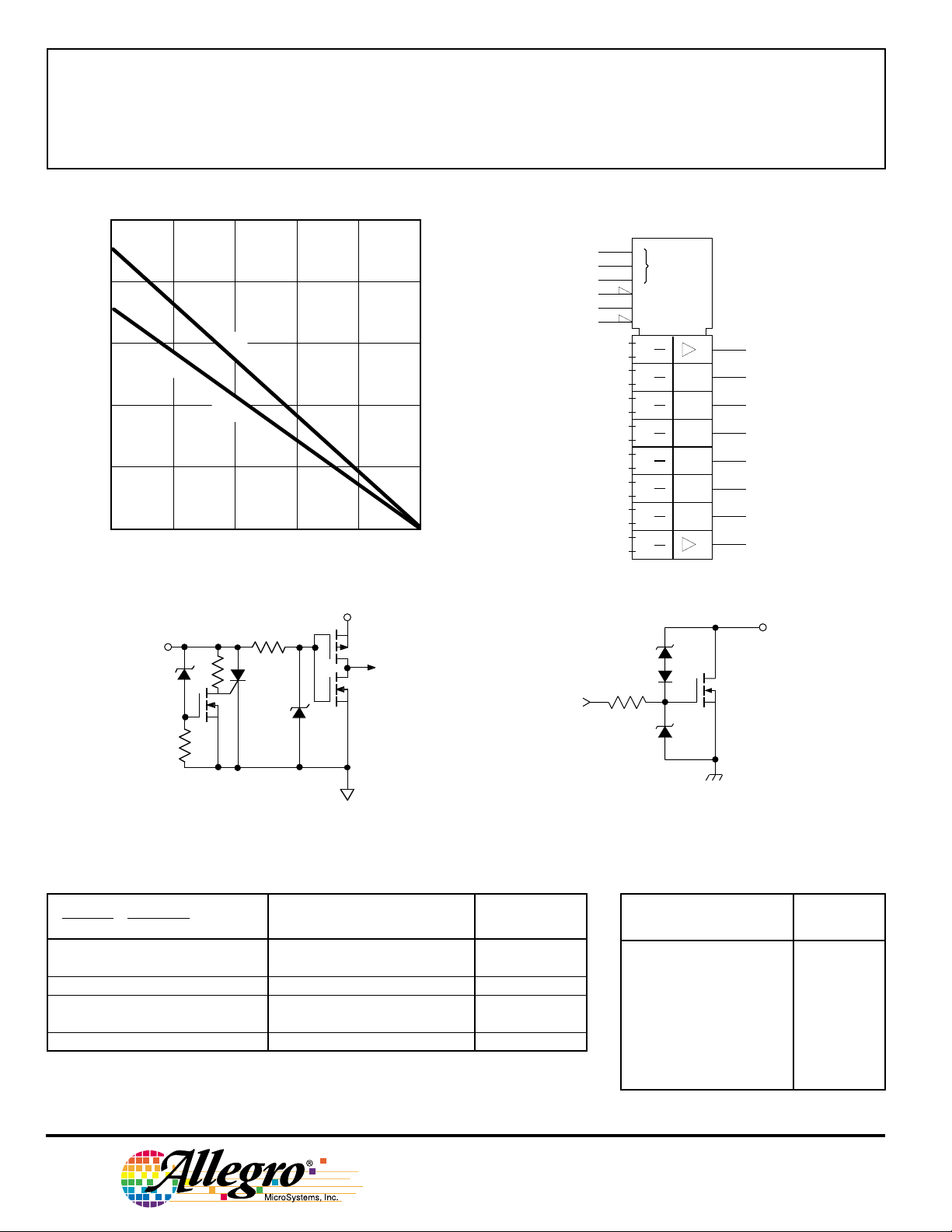
DMOS POWER DRIVER
2.5
2.0
SUFFIX 'A', R = 55
1.5
1.0
SUFFIX 'LW
θ
J
A
', R = 70
θ
J
A
°C/W
°C/W
0.5
0
25
ALLOWABLE PACKAGE POWER DISSIPATION IN WATTS
50 75 100 125 150
AMBIENT TEMPERATURE IN °C
Dwg. GS-004A
V
DD
IN
LOGIC SYMBOL
3
8
12
13
18
19
0
2
G8
Z9
Z10
9,0D
10,0R
9,1D
10,1R
9,2D
10,2R
9,3D
10,3R
9,4D
10,4R
9,5D
10,5R
9,6D
10,6R
9,7D
10,7R
8M 0/7
Dw
4
5
6
7
14
15
16
17
. FP-046
OUT
Dwg. EP-010-15
FUNCTION TABLE
Inputs
CLEAR ENABLE DATA OUTPUT OUTPUTs Function
HLH L R
HLL H R
H H X R R Memory
LLH L H
LLL H H
L H X H H Clear
L = Low Logic Level H = High Logic Level X = Irrelevant R = Previous State
Addressed Other
115 Northeast Cutoff, Box 15036
Worcester, Massachusetts 01615-0036 (508) 853-5000
W
Copyright © 2000, Allegro MicroSystems, Inc.
DMOS POWER DRIVER OUTPUTLOGIC INPUTS
Addressable
Latch
8-Line
Demultiplexer
Dwg. EP-063
LATCH SELECTION TABLE
Select Inputs
S2 (MSB)S1S0 (LSB) OUTPUT
LLL 0
LLH 1
LHL 2
LHH 3
HLL 4
HLH 5
HHL 6
HHH 7
Addressed
8-BIT ADDRESSABLE
DMOS POWER DRIVER
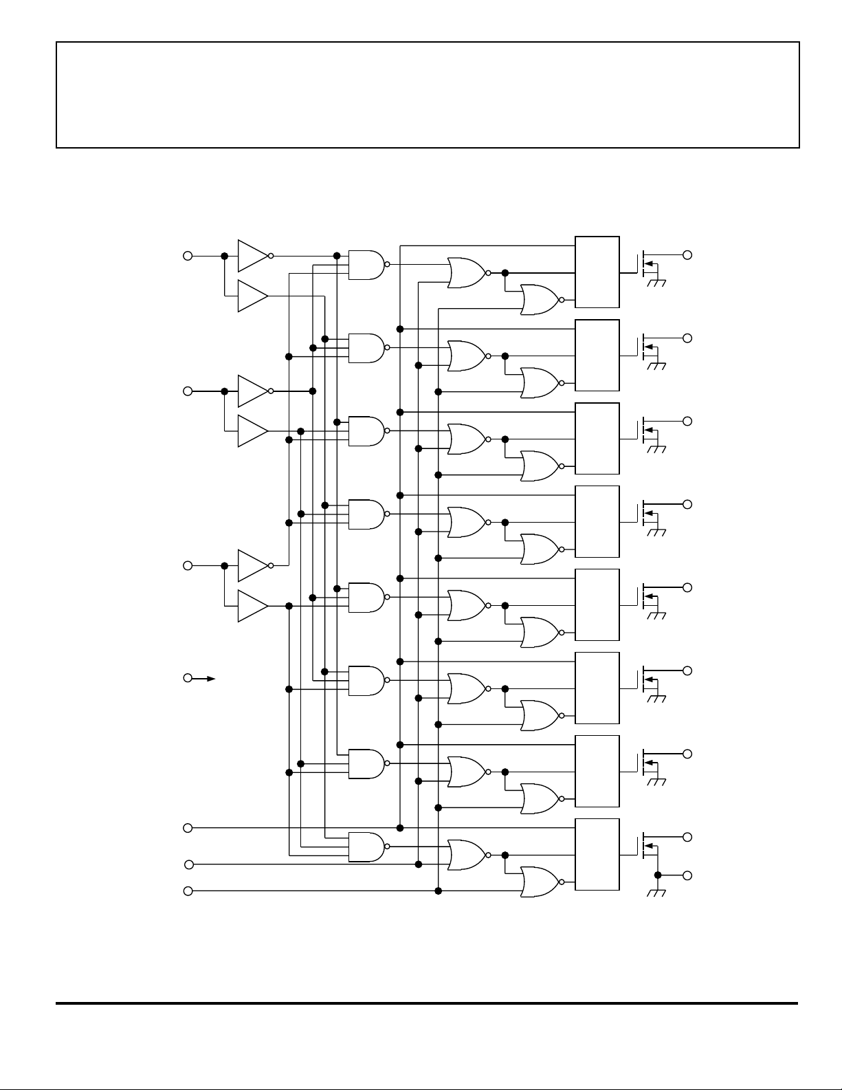
FUNCTIONAL BLOCK DIAGRAM
6B259
(LSB)
(MSB)
S
0
S
1
S
2
D
C1
CLR
D
C1
CLR
D
C1
CLR
D
C1
CLR
D
C1
CLR
OUT
OUT
OUT
OUT
OUT
0
1
2
3
4
LOGIC
SUPPLY
DATA
ENABLE
(ACTIVE LOW)
CLEAR
(ACTIVE LOW)
www.allegromicro.com
D
V
DD
C1
CLR
D
C1
CLR
D
C1
CLR
Grounds (terminals 9, 10, and 11) must be connected externally to a single point.
OUT
5
OUT
6
OUT
7
GROUND
Dwg. FP-047
6B259
8-BIT ADDRESSABLE
DMOS POWER DRIVER
RECOMMENDED OPERATING CONDITIONS
over operating temperature range
Logic Supply Voltage Range, VDD............... 4.5 V to 5.5 V
High-Level Input Voltage, V
Low-level input voltage, V
............................ ≥ 0.85V
IH
................................. ≤0.15V
IL
DD
DD
ELECTRICAL CHARACTERISTICS at T
= +25°C, V
A
= 5 V, tir = t
DD
≤ 10 ns (unless otherwise
if
specified).
Limits
Characteristic Symbol Test Conditions Min. Typ. Max. Units
Logic Supply Voltage V
Output Breakdown V
(BR)DSXIO
Voltage
Off-State Output I
Current
Static Drain-Source r
On-State Resistance
Nominal Output I
Current
Logic Input Current I
Prop. Delay Time t
DD
DSX
DS(on)
ON
IH
I
IL
PLH
Operating 4.5 5.0 5.5 V
= 1 mA 50 — — V
VO = 40 V, V
VO = 40 V, VDD = 5.5 V, T
IO = 100 mA, V
IO = 100 mA, VDD = 4.5 V, T
IO = 350 mA, V
V
= 0.5 V, T
DS(on)
VI = V
DD
VI = 0, V
= 5.5 V — 0.1 5.0 µA
DD
= 125°C — 0.15 8.0 µA
A
= 4.5 V — 4.2 5.7 Ω
DD
= 125°C— 6.8 9.5 Ω
A
= 4.5 V (see note) — 5.5 8.0 Ω
DD
= 85°C—90—mA
A
= 5.5 V — — 1.0 µA
= 5.5 V — — -1.0 µA
DD
IO = 100 mA, CL = 30 pF — 150 — ns
Output Rise Time t
Output Fall Time t
Supply Current I
DD(OFF)
I
DD(ON)
t
PHL
r
f
IO = 100 mA, CL = 30 pF — 90 — ns
IO = 100 mA, CL = 30 pF — 200 — ns
IO = 100 mA, CL = 30 pF — 200 — ns
V
= 5.5 V, Outputs off — 20 100 µA
DD
V
= 5.5 V, Outputs on — 150 300 µA
DD
Typical Data is at VDD = 5 V and is for design information only.
NOTE — Pulse test, duration ≤100 µs, duty cycle ≤2%.
115 Northeast Cutoff, Box 15036
Worcester, Massachusetts 01615-0036 (508) 853-5000
 Loading...