

ALLEGRO A6841 User Manual

A6841
DABiC-5 8-Bit Serial Input Latched Sink Drivers
The merging of low-power CMOS logic and bipolar output power
drivers permit the A6841 integrated circuits to be used in a wide variety
of peripheral power driver applications. Each device has an eight-bit
Package A
18-pin DIP
CMOS shift register and CMOS control circuitry, eight CMOS data
latches, and eight bipolar current-sinking Darlington output drivers. The
500 mA NPN Darlington outputs, with integral transient-suppression
diodes, are suitable for use with relays, solenoids, and other inductive
loads.
All package variations of the A6841 offer premium performance with
a minimum output-breakdown voltage rating of 50 V (35 V sustaining).
All drivers can be operated with a split supply where the negative supply is up to –20 V.
26185.114B
Data Sheet
Package LW
18-pin Wide Body SOIC
Package LW-20
20-pin Wide Body SOIC
AB SO LUTE MAX I MUM RAT INGS
Output Voltage
VCE..............................................................50 V
V
Logic Supply Voltage, V
Emitter Supply Voltage, V
Input Voltage Range, V
Continuous Output Current (each output), I
Package Power Dissipation, P
Operating Temperature Range
Ambient Temperature, T
Storage Temperature, TS..........–55°C to +150°C
Caution: CMOS devices have input-static protection,
but are susceptible to damage when exposed to
extremely high static-electrical charges.
(for inductiove load applications) .......35 V
CE(SUS)
...................................7 V
DD
.............................–20 V
EE
..............–0.3 V to VDD +0.3 V
IN
, see chart, page 6
D
............–20°C to +85°C
A
OUT
...500 mA
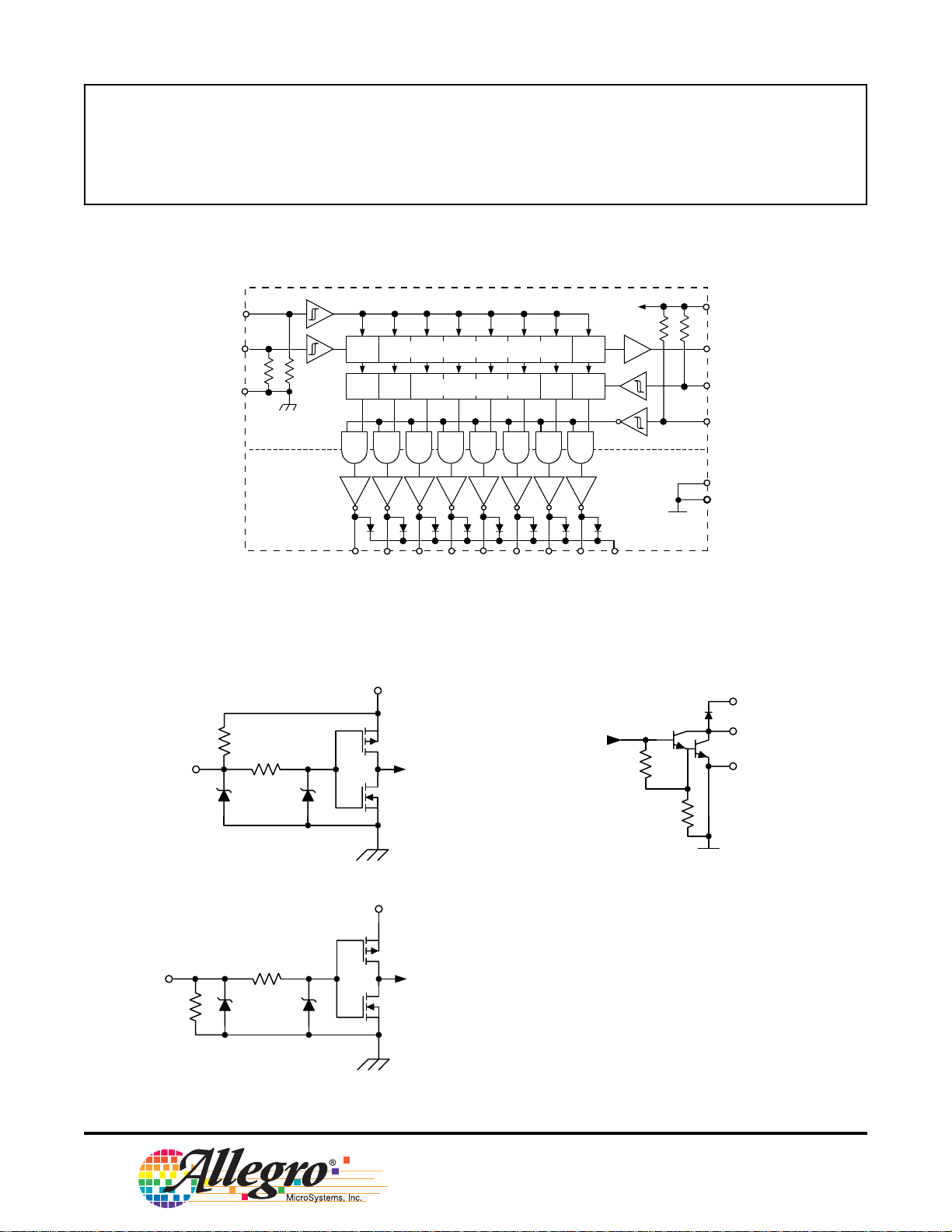
The CMOS inputs are compatible with standard CMOS logic levels.
TTL circuits may require the use of appropriate pull-up resistors. By
using the serial data output, drivers can be cascaded for interface applications requiring additional drive lines.
The A6841SA devices are furnished in a standard 18-pin plastic DIP. The
A6841SL W device is available in an 18-lead SOIC package. A 20-pin
SOIC version, A6841SLW-20 has improved thermal characteristics. The
SOIC drivers are also available for operation to a temperature of –40°C
(part number suffi x EL W). These devices are lead (Pb) free, with 100%
matte tin plated leadframes.
FEATURES
3.3 V to 5 V logic supply range
Power on reset (POR)
To 10 MHz data input rate
CMOS, TTL compatible inputs
–40°C operation available
Low-power CMOS logic and latches
Schmitt trigger inputs for
improved noise immunity
High-voltage current-sink outputs
Internal pull-up/pull down resistors
Output transient-protection diodes
Single or split supply operation
APPLICATIONS
Relays
Solenoids
Inductive loads
Use the following complete part numbers when ordering:
Part Number Package Ambient
A6841SA-T 18-pin DIP –20ºC to +85ºC
A6841SLW-T 18-pin wide body SOIC –20ºC to +85ºC
A6841SLW-20-T
A6841ELW-T 18-pin wide body SOIC –40ºC to +85ºC
A6841ELW-20-T
20-pin wide body SOIC
(enhanced thermals)
20-pin wide body SOIC
(enhanced thermals)
–20ºC to +85ºC
–40ºC to +85ºC
A6841
OUT
SUB
K
V
EE
DABiC-5 8-Bit Serial Input Latched Sink Drivers
Functional Block Diagram
26185.114B
Data Sheet
CLOCK
SERIAL
DATA IN
LOGIC
GROUND
Typical Input Circuits
STROBE
OUTPUT
ENABLE
S E R IAL-P AR AL L E L S HIF T RE G IS T E R
OUT1OUT2OUT
V
DD
LATCHE S
OUT4OUT
3
OUT6OUT7OUT
5
LOGIC
V
DD
BIPOLAR
K
8
SUPPLY
SERIAL
DATA OUT
STROBE
OUTPUT E NABLE
(ACT IVE LOW )
MOS
VEE or POWER GROUND
VEE or POWER GROUND
SUB
Typical Output Driver
CLOCK
SERIAL
DATA IN
V
DD
www.allegromicro.com
115 Northeast Cutoff, Box 15036
Worcester, Massachusetts 01615-0036 (508) 853-5000
2
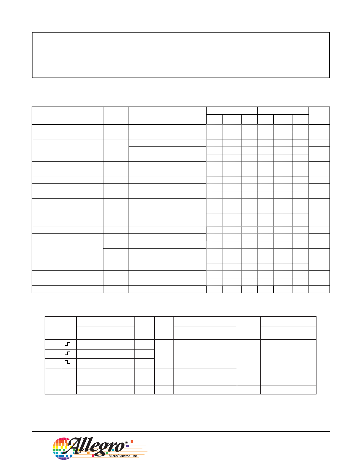
A6841
Serial Shift Register Contents Serial Latch Contents Output Output Contents
Data Clock Data Strobe Enable
Input Input I
1I2I3
... I
8
Output Input I1I2I3... I
8
Input I1I2I3... I
8
R
7
R
7
R
1R2R3
... R
8
R
8
XXX...X XXL
R
1R2
... R
7
L
L
R
1R2R3
... R
8
P1P2P3... P
8
P
8
P1P2P3... P
81
P2P3... P
8
XXX...X
L
P
HH
H
H
H
R
1R2
... R
7
H
H
H...
DABiC-5 8-Bit Serial Input Latched Sink Drivers
26185.114B
Data Sheet
ELECTRICAL CHARACTERISTICS1 Unless otherwise noted: T
= 25°C, V
A
= 0 V, logic supply operating
ee
voltage Vdd = 3.0 V to 5.5 V
V
= 3.3 V Vdd = 5 V
dd
Characteristic Symbol Test Conditions
Output Leakage Current I
Output Sustaining Voltage V
Collector–Emitter Saturation
Voltage
Input Voltage
CE(SUS)IOUT
V
CE(SAT)
V
V
Input Resistance R
V
Serial Data Output Voltage
Maximum Clock Frequency
Logic Supply Current
2
OUT(1)IOUT
V
OUT(0)IOUT
I
DD(1)
I
DD(0)
Clamp Diode Leakage Current I
Clamp Diode Forward Voltage V
t
Output Enable-to-Output Delay
Strobe-to-Output Delay
dis(BQ)VCC
t
en(BQ)VCC
t
p(STH-QL)VCC
t
p(STH-QH)VCC
Output Fall Time t
Output Rise Time t
Clock-to-Serial Data Out Delay t
1
Positive (negative) current is defi ned as conventional current going into (coming out of) the specifi ed device pin.
2
Operation at a clock frequency greater than the specifi ed minimum value is possible but not warranteed.
p(CH-SQX)IOUT
V
CEX
= 50 V – – 10 – – 10 μA
OUT
= 350 mA, L = 3 mH 35 – – 35 – – V
I
= 100 mA – – 1.1 – – 1.1 V
OUT
= 200 mA – – 1.3 – – 1.3 V
I
OUT
I
= 350 mA – – 1.6 – – 1.6 V
OUT
IN(1)
IN(0)
IN
= –200 μA 2.8 3.05 – 4.5 4.75 – V
= 200 μA – 0.15 0.3 – 0.15 0.3 V
f
c
One output on, OE = L, ST = H – – 2.0 – – 2.0 mA
All outputs off, OE = H, ST = H,
P1 through P8 = L
Vr = 50 V – – 50 – – 50 μA
r
If = 350 mA – – 2 – – 2 V
f
= 50 V, R1 = 500 Ω, C1 ≤ 30 pF – – 1.0 – – 1.0 μs
= 50 V, R1 = 500 Ω, C1 ≤ 30 pF – – 1.0 – – 1.0 μs
= 50 V, R1 = 500 Ω, C1 ≤ 30 pF – – 1.0 – – 1.0 μs
= 50 V, R1 = 500 Ω, C1 ≤ 30 pF – – 1.0 – – 1.0 μs
VCC = 50 V, R1 = 500 Ω, C1 ≤ 30 pF – – 1.0 – – 1.0 μs
f
VCC = 50 V, R1 = 500 Ω, C1 ≤ 30 pF – – 1.0 – – 1.0 μs
r
= ±200 μA – 50 – – 50 – ns
Min. Typ. Max. Min. Typ. Max.
2.2 – – 3.3 – – V
– – 1.1 – – 1.7 V
50 – – 50 – – kΩ
10 – – 10 – – MHz
– – 100 – – 100 μA
Units
Truth Table
L = Low Logic Level
H = High Logic Level
X = Irrelevant
P = Present State
R = Previous State
OE = Output Enable
ST = Strobe
www.allegromicro.com
115 Northeast Cutoff, Box 15036
Worcester, Massachusetts 01615-0036 (508) 853-5000
3
 Loading...