

A6821
DABiC-5 8-Bit Serial Input Latched Sink Drivers
A merged combination of bipolar and MOS technology gives these
devices an interface fl exibility beyond the reach of standard logic
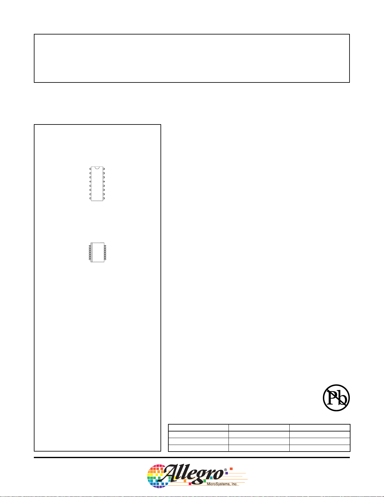
Package A
16-pin DIP
buffers and power driver arrays. Typical applications include driving
multiplexed LED displays or incandescent lamps.
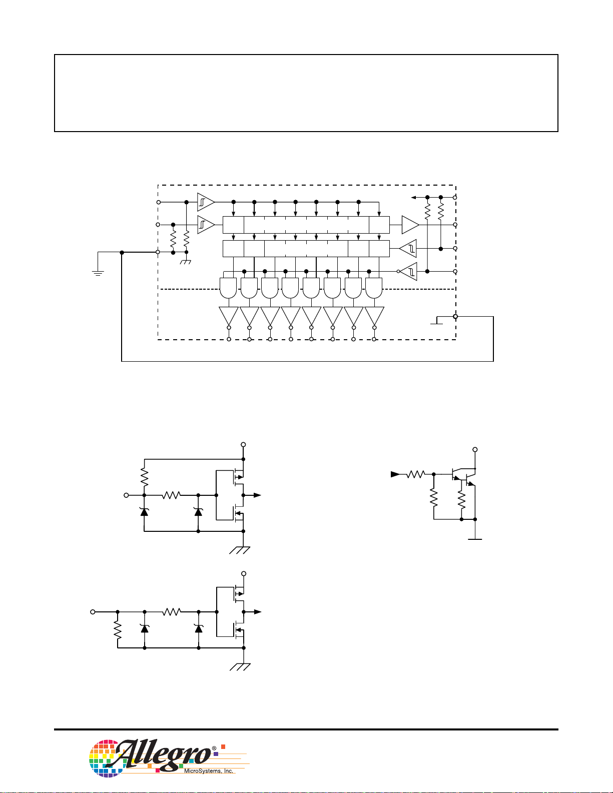
The A6821 has an eight-bit CMOS shift register and CMOS control
circuitry, eight CMOS data latches, and eight bipolar current-sinking
Darlington output drivers.
The CMOS inputs are compatible with standard CMOS logic levels.
TTL circuits may require the use of appropriate pull-up resistors. By
using the serial data output, the drivers can be cascaded for interface
applications requiring additional drive lines.
26185.112B
Data Sheet
Package LW
16-pin Wide Body SOIC
AB SO LUTE MAX I MUM RAT INGS
Output Voltage, V
Logic Supply Voltage, V
Input Voltage Range, V
Continuous Output Current (each output), I
Package Power Dissipation, P
A6821SA/A6821EA..................................2.1 W
A6821SLW............................................... 1.5 W
Operating Temperature Range
Ambient Temperature, T
Storage Temperature, TS..........–55°C to +150°C
Caution: CMOS devices have input-static protection,
but are susceptible to damage when exposed to
extremely high static-electrical charges.
.........................................50 V
OUT
...................................7 V
DD
..............–0.3 V to VDD +0.3 V
IN
OUT
D
............–20°C to +85°C
A
...500 mA
The A6821SA is furnished in a standard 16-pin plastic DIP. The
A6821EA is a 16-pin plastic DIP, capable of operation from -40°C to
+85°C. The A6821SLW is a 16-lead wide-body SOIC, for surfacemount applications. These devices are lead (Pb) free, with 100% matte
tin plated leadframes.
FEATURES
3.3 V to 5 V logic supply range
Power on reset (POR)
To 10 MHz data input rate
CMOS, TTL compatible
–40°C operation available
Schmitt trigger inputs for improved
noise immunity
Low-power CMOS logic and latches
High-voltage current-sink outputs
Internal pull-up/pull down resistors
APPLICATIONS
Multiplexed LED displays
Incandescent lamps
Use the following complete part numbers when ordering:
Part Number Package Ambient
A6821SA-T 16-pin DIP –20ºC to +85ºC
A6821EA-T 16-pin DIP –40ºC to +85ºC
A6821SLW-T 16-pin wide body SOIC –20ºC to +85ºC
A6821
OUT
7.2 k 3 k
SUB
DABiC-5 8-Bit Serial Input Latched Sink Drivers
Functional Block Diagram
26185.112B
Data Sheet
CLOCK
SERIAL
DATA IN
LOGIC
GROUND
Typical Input Circuits
STROBE
OUTPUT
ENABLE
OUT1OUT
V
S E R IAL-P AR ALLE L SHIF T R E G IS T E R
LATCHE S
OUT4OUT
OUT
2
3
DD
OUT6OUT7OUT
5
LOGIC
MOS
SUB
SUPPLY
SERIAL
DATA O UT
STROBE
OUTPUT E NABLE
(ACT IVE L O W )
POWER
GROUND
V
DD
BIPOLAR
8
Typical Output Driver
ΩΩ
CLOCK
SERIAL
DATA IN
V
DD
www.allegromicro.com
115 Northeast Cutoff, Box 15036
Worcester, Massachusetts 01615-0036 (508) 853-5000
2
A6821
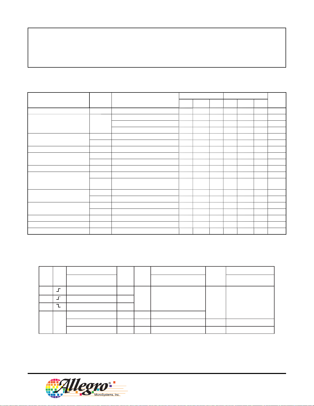
Serial Shift Register Contents Serial Latch Contents Output Output Contents
Data Clock Data Strobe Enable
Input Input I
1I2I3
... I
8
Output Input I1I2I3... I
8
Input I1I2I3... I
8
R
7
R
7
R
1R2R3
... R
8
R
8
XXX...X XXL
R
1R2
... R
7
L
L
R
1R2R3
... R
8
P1P2P3... P
8
P
8
P1P2P3... P
81
P2P3... P
8
XXX...X
L
P
HH
H
H
H
R
1R2
... R
7
H
H
H...
DABiC-5 8-Bit Serial Input Latched Sink Drivers
26185.112B
Data Sheet
ELECTRICAL CHARACTERISTICS1 Unless otherwise noted: T
Characteristic Symbol Test Conditions
Output Leakage Current I
Collector–Emitter Saturation
Voltage
Input Voltage
V
CE(SAT)
V
V
Input Resistance R
V
Serial Data Output Voltage
Maximum Clock Frequency
Logic Supply Current
Output Enable-to-Output Delay
Strobe-to-Output Delay
2
OUT(1)IOUT
V
OUT(0)IOUT
I
DD(1)
I
DD(0)
t
dis(BQ)VCC
t
en(BQ)
t
p(STH-QL)VCC
t
p(STH-QH)VCC
Output Fall Time t
Output Rise Time t
Clock-to-Serial Data Out Delay t
1
Positive (negative) current is defi ned as conventional current going into (coming out of) the specifi ed device pin.
2
Operation at a clock frequency greater than the specifi ed minimum value is possible but not warranteed.
p(CH-SQX)IOUT
V
CEX
IN(1)
IN(0)
IN
= 50 V – – 10 – – 10 μA
OUT
I
= 100 mA – – 1.1 – – 1.1 V
OUT
I
= 200 mA – – 1.3 – – 1.3 V
OUT
= 350 mA – – 1.6 – – 1.6 V
I
OUT
= –200 μA 2.8 3.05 – 4.5 4.75 – V
= 200 μA – 0.15 0.3 – 0.15 0.3 V
f
c
One output on, OE = L, ST = H – – 2.0 – – 2.0 mA
All outputs off, OE = H, ST = H,
P1 through P8 = L
= 50 V, R1 = 500 Ω, C1 ≤ 30 pF – – 1.0 – – 1.0 μs
VCC = 50 V, R1 = 500 Ω, C1 ≤ 30 pF – – 1.0 – – 1.0 μs
= 50 V, R1 = 500 Ω, C1 ≤ 30 pF – – 1.0 – – 1.0 μs
= 50 V, R1 = 500 Ω, C1 ≤ 30 pF – – 1.0 – – 1.0 μs
VCC = 50 V, R1 = 500 Ω, C1 ≤ 30 pF – – 1.0 – – 1.0 μs
f
VCC = 50 V, R1 = 500 Ω, C1 ≤ 30 pF – – 1.0 – – 1.0 μs
r
= ±200 μA – 50 – – 50 – ns
= 25°C, logic supply operating voltage V
A
V
= 3.3 V Vdd = 5 V
dd
Min. Typ. Max. Min. Typ. Max.
2.2 – – 3.3 – – V
– – 1.1 – – 1.7 V
50 – – 50 – – kΩ
10 – – 10 – – MHz
– – 100 – – 100 μA
= 3.0 V to 5.5 V
dd
Units
Truth Table
L = Low Logic Level
H = High Logic Level
X = Irrelevant
P = Present State
R = Previous State
OE = Output Enable
ST = Strobe
www.allegromicro.com
115 Northeast Cutoff, Box 15036
Worcester, Massachusetts 01615-0036 (508) 853-5000
3
A6821
DABiC-5 8-Bit Serial Input Latched Sink Drivers
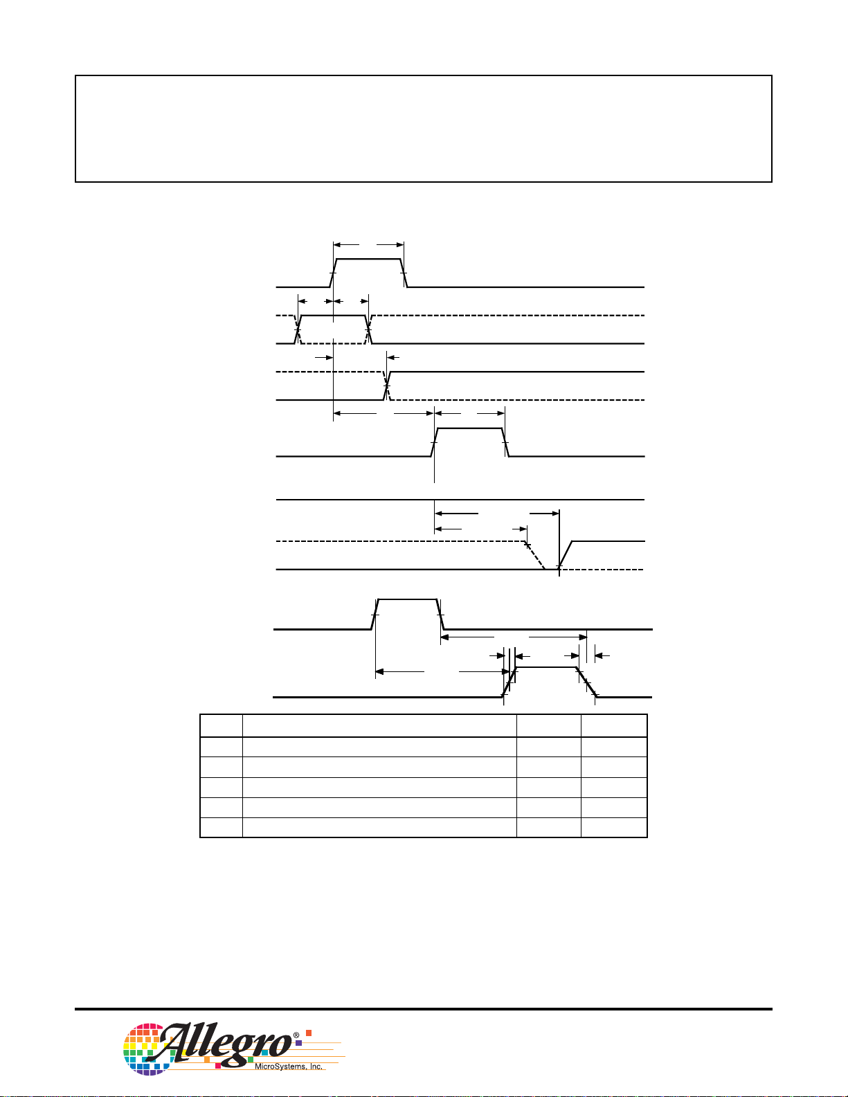
Timing Requirements and Specifi cations
(Logic Levels are VDD and Ground)
C
26185.112B
Data Sheet
CLOCK
SERIAL
DATA IN
SERIAL
DATA OUT
STROBE
OUTPUT ENABLE
OUTPUT ENABLE
OUT
OUT
50%
A B
DATA
N
N
50%
t
p(CH-SQX)
50%
D E
50%
LOW = ALL OUTP UTS E NABLE D
t
p(STH-QH)
t
p(STH-QL)
HIGH = ALL OUTP UTS BLANKE D (DIS ABLE D)
50%
t
dis(BQ)
10%
DATA
t
en(BQ)
90%
t
r
DATA
10%
90%
50%
DATA
t
f
Key Description Symbol Time (ns)
A Data Active Time Before Clock Pulse (Data Set-Up Time)
B Data Active Time After Clock Pulse (Data Hold Time)
C Clock Pulse Width
D Time Between Clock Activation and Strobe
E Strobe Pulse Width
NOTE: Timing is representative of a 10 MHz clock. Higher speeds may be
attainable; operation at high temperatures will reduce the specifi ed maxi-
mum clock frequency.
Powering-on with the inputs in the low state ensures that the registers and
latches power-on in the low state (POR).
Serial Data present at the input is transferred to the shift register on the logical
0 to logical 1 transition of the CLOCK input pulse. On succeeding CLOCK
pulses, the registers shift data information towards the SERIAL DATA OUTPUT. The SERIAL DATA must appear at the input prior to the rising edge of the
CLOCK input waveform.
www.allegromicro.com
115 Northeast Cutoff, Box 15036
Worcester, Massachusetts 01615-0036 (508) 853-5000
t
su(D)
t
h(D)
t
w(CH)
t
su(C)
t
w(STH)
25
25
50
100
50
Information present at any register is transferred to the respective latch
when the STROBE is high (serial-to-parallel conversion). The latches will
continue to accept new data as long as the STROBE is held high. Applications where the latches are bypassed (STROBE tied high) will require that
the OUTPUT ENABLE input be high during serial data entry.
When the OUTPUT ENABLE input is high, all of the output buffers are
disabled (OFF). The information stored in the latches or shift register is not
affected by the OUTPUT ENABLE input. With the OUTPUT ENABLE
input low, the outputs are controlled by the state of their respective latches.
4
A6821
DABiC-5 8-Bit Serial Input Latched Sink Drivers
26185.112B
Data Sheet
Maximum Allowable Duty Cycle, I
Number of
Outputs ON
A6821SA/A6821EA
25°C40°C50°C60°C70°C
8 90% 79% 72% 65% 57%
7 100% 90% 82% 74% 65%
6 100% 100% 96% 86% 76%
5 100% 100% 100% 100% 91%
4 100% 100% 100% 100% 100%
3 100% 100% 100% 100% 100%
2 100% 100% 100% 100% 100%
1 100% 100% 100% 100% 100%
A6821SLW
8 67% 59% 54% 49% 43%
7 77% 68% 62% 56% 49%
6 90% 79% 72% 65% 57%
5 100% 95% 86% 78% 68%
4 100% 100% 100% 98% 86%
3 100% 100% 100% 100% 100%
2 100% 100% 100% 100% 100%
1 100% 100% 100% 100% 100%
Am bient T emper ature
Terminal List Table
= 200 mA, VDD = 5 V
OUT
Name Description Pin
CLK Clock 1
Serial Data In 2
Logic Ground* 3
VDD Logic Supply 4
Serial Data Out 5
ST Strobe 6
OE Output Enable (active low) 7
SUB Power Ground* 8
OUT
OUT
OUT
OUT
OUT
OUT
OUT
OUT
8
7
6
5
4
3
2
1
Serial Data Output 9
Serial Data Output 10
Serial Data Output 11
Serial Data Output 12
Serial Data Output 13
Serial Data Output 14
Serial Data Output 15
Serial Data Output 16
* There is an indeterminate resistance between logic ground and power ground.
For proper operation, these terminals must be externally connected together.
www.allegromicro.com
115 Northeast Cutoff, Box 15036
Worcester, Massachusetts 01615-0036 (508) 853-5000
5
A6821
DABiC-5 8-Bit Serial Input Latched Sink Drivers
26185.112B
Data Sheet
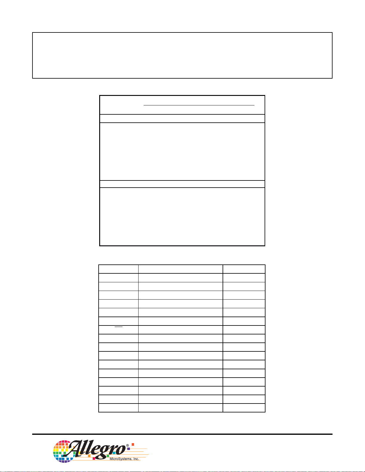
CLOCK CLK
SERIAL
DATA IN
LOGIC
GROUND
LOGIC
SUPPLY
SERIAL
DATA OUT
STROBE
OUTPUT
ENABLE
POWER
GROUND
Package A
16-pin DIP
1
2
3
4
V
DD
5
LATCHES
SHIFT REGISTER
6
ST
7
OE
8
SUB
16 OUT
15
OUT
OUT
14
13
OUT
12
OUT
11
OUT
OUT
10
OUT
9
1
2
3
4
5
6
7
8
CLOCK CLK
SERIAL
DATA IN
LOGIC
GROUND
LOGIC
SUPPLY
SERIAL
DATA OUT
STROBE
OUTPUT
ENABLE
POWER
GROUND
1
2
3
4
5
6
7
8
Package LW
16-pin Wide Body SOIC
V
DD
LATCHE S
ST
OE
SUB
S HIF T R E G IS TE R
16 OUT
15
OUT
OUT
14
13
OUT
12
OUT
11
OUT
OUT
10
OUT
9
1
2
3
4
5
6
7
8
www.allegromicro.com
115 Northeast Cutoff, Box 15036
Worcester, Massachusetts 01615-0036 (508) 853-5000
6
A6821
DABiC-5 8-Bit Serial Input Latched Sink Drivers
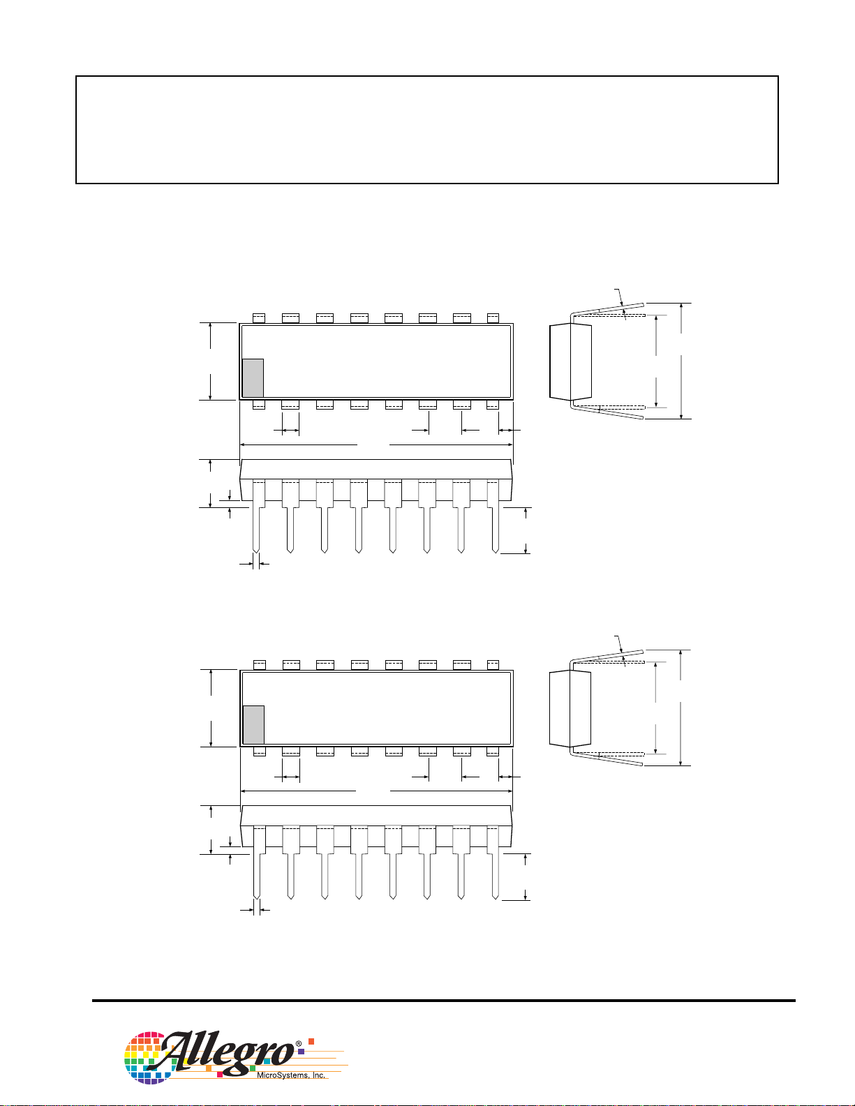
Package A
16-pin DIP
Dimensions in Inches
(controlling dimensions)
0.014
0.008
0.300
BSC
0.430
MAX
0.280
0.240
16
9
26185.112B
Data Sheet
0.210
MAX
7.11
6.10
0.015
MIN
1
0.070
0.045
16
1
1.77
1.15
0.022
0.014
8
0.775
0.735
0.100
BSC
Dimensions in Millimeters
(for reference only)
9
8
19.68
18.67
2.54
BSC
0.005
0.150
0.115
0.13
MIN
MIN
0.355
0.204
Dwg. MA-001-16A in
10.92
MAX
7.62
BSC
5.33
MAX
0.39
MIN
0.558
0.356
NOTES: 1. Lead thickness is measured at seating plane or below.
2. Lead spacing tolerance is non-cumulative.
3. Exact body and lead configuration at vendor’s option within limits shown.
www.allegromicro.com
115 Northeast Cutoff, Box 15036
Worcester, Massachusetts 01615-0036 (508) 853-5000
3.81
2.93
Dwg. MA-001-16A mm
7

A6821
DABiC-5 8-Bit Serial Input Latched Sink Drivers
Package LW
16-pin Wide Body SOIC
Dimensions in Inches
(for reference only)
26185.112B
Data Sheet
0.2992
0.2914
0.020
0.013
0.0926
0.1043
16 9
1 2
3
0.4133
0.3977
0.0040
MIN.
Dimensions in Millimeters
(controlling dimensions)
0.0125
0.0091
0.419
0.394
0.050
0.016
0.050
BSC
916
0°TO 8°
Dwg. MA-008-16A in
0.32
0.23
7.60
7.40
0.51
1 2
0.33
2.65
2.35
0.10
3
MIN.
NOTES: 1. Lead spacing tolerance is non-cumulative.
2. Exact body and lead configuration at vendor’s option within limits shown.
10.65
10.00
1.27
10.50
10.10
BSC
0°TO 8°
www.allegromicro.com
115 Northeast Cutoff, Box 15036
Worcester, Massachusetts 01615-0036 (508) 853-5000
1.27
0.40
Dwg. MA-008-16A mm
8

A6821
DABiC-5 8-Bit Serial Input Latched Sink Drivers
26185.112B
Data Sheet
The products described here are manufactured under one or
more U.S. patents or U.S. patents pending.
Allegro MicroSystems, Inc. reserves the right to make, from time
to time, such de par tures from the detail spec i fi ca tions as may be
required to permit improvements in the per for mance, reliability,
or manufacturability of its products. Before placing an order, the
user is cautioned to verify that the information being relied upon is
current.
Allegro products are not authorized for use as critical components in life-support devices or sys tems without express written
approval.
The in for ma tion in clud ed herein is believed to be ac cu rate and
reliable. How ev er, Allegro MicroSystems, Inc. assumes no re spon si bil i ty for its use; nor for any in fringe ment of patents or other
rights of third parties which may result from its use.
Copyright©2004, 2005 AllegroMicrosystems, Inc.
www.allegromicro.com
115 Northeast Cutoff, Box 15036
Worcester, Massachusetts 01615-0036 (508) 853-5000
9
 Loading...