

Page 1

A6285
16-Channel Constant-Current Latched LED Driver
with Open LED Detection and Dot Correction
Features and Benefits
▪ 3.0 to 5.5 V logic supply range
▪ Schmitt trigger inputs for improved noise immunity
▪ Power-On Reset (POR)
▪ Up to 80 mA constant-current sinking outputs
▪ LED open circuit detection (LOD)
▪ Dot correction (DC) for adjusting LED light intensity on
each channel with 7-bit resolution
▪ Low-power CMOS logic and latches
▪ High data input rate up to 30 MHz
▪ Active output pull-ups with enable/disable
▪ 20 ns typical staggering delay between outputs
▪ Internal UVLO and thermal shutdown (TSD) circuitry
▪ Fault output flags for an LED open circuit (LOD) or a
thermal shutdown (TSD) condition
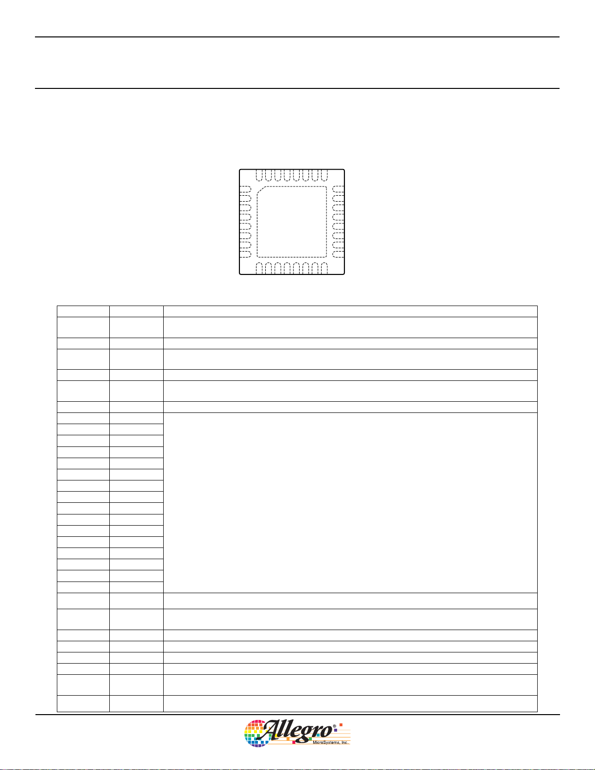
Package: 32 Contact QFN (suffix ET)
5 mm × 5 mm
0.90 mm nominal overall height
Description
The A6285 is designed for LED display applications. This
BiCMOS device includes an On/Off shift register, a Dot
Correction (DC) shift register, accompanying data latches, and
16 MOS constant-current sink drivers with active pull-ups that
can be enabled or disabled as required by the application.
The CMOS shift registers and latches allow direct interfacing
with microprocessor-based systems. With a 3.3 or 5 V logic
supply, typical serial data input rates can reach up to 30 MHz.
The LED drive current level can be set by a single external
resistor, selected by the application designer. A CMOS serial
data output permits cascading of multiple devices in applications
requiring additional drive lines.
Individual LED light intensity can be adjusted to correct for light
intensity variations by using the Dot Correction feature.
Open LED connections can be detected, and then signaled back
to the host microprocessor through the serial data output (SDO
pin). The FAULT output flags an LED open circuit (LOD)
condition or a thermal shutdown (TSD) condition. A staggering
delay on the load outputs during ON/OFF transitions helps to
reduce ground bounce.
Continued on the next page…
Not to scale
Controller
T ypical Application
V
DD
100 KΩ
SDI SDI
FAULT
CLK
LE
MODE
OE
SDO
FAULT
CLK
LE
MODE
OE
V
LED
PE
OUT0 OUT15
A6285
V
LED
10 μF
SDO
V
DD
100 nF
REXT
6285-DS, Rev. 1
Page 2

16-Channel Constant-Current Latched LED Driver
A6285
with Open LED Detection and Dot Correction
Description (continued)
The device is available in a 32-lead QFN (package ET), with an
exposed thermal pad. It is lead (Pb) free with 100% matte tin
leadframe plating.
Selection Guide
Part Number Package Packing (estimated)
A6285EET-T 5×5 mm QFN, 32 pin, exposed thermal pad 73 pieces per tube
A6285EETTR-T 5×5 mm QFN, 32 pin, exposed thermal pad 1500 pieces per 7-in reel
Applications include the following:
▪ Display backlighting
▪ Monocolor, multicolor, or full-color LED display
▪ Monocolor, multicolor, LED Signboard
▪ Multicolor LED lighting
Absolute Maximum Ratings
Characteristic Symbol Notes Min. Max. Unit
Supply Voltage* V
OUTx Current (any single output) I
Input Voltage Range* V
LED Load Supply Range* V
ESD Rating
Operating Temperature Range (E) T
Junction Temperature T
Storage Temperature Range T
*With respect to ground (GND, PGND).
DD
O
VOE, VLE, V
I
LED
HBM (JEDEC JESD22-A114, Human Body Model) – 1.5 kV
CDM (JEDEC JESD22-C101, Charged Device Model) – 1.0 kV
A
(max) – 150 °C
J
stg
CLK
, V
SDI
, V
MODE
–0.3 5.5 V
–90mA
–0.3 VDD + 0.3 V
–0.3 13.2 V
–40 85 °C
–55 150 °C
Allegro MicroSystems, Inc.
115 Northeast Cutoff
Worcester, Massachusetts 01615-0036 U.S.A.
1.508.853.5000; www.allegromicro.com
2
Page 3

A6285
16-Channel Constant-Current Latched LED Driver
with Open LED Detection and Dot Correction
Functional Block Diagram
MODE
CLK
SDI
OE
REXT
GND
LE
TSD
UVLO
01 15
1
MODE
0
1
MODE
0
1
ON/OFF Shift Register
0
MODE
015
1
0
MODE
ON/OFF
Register
0
LOD
0
Io
Regulator
LE
DC Register
06
7-Bit
DC
015
LOD
1
Status Info:
LOD
ON/OFF
Register
1
TSD
LOD
VDD
DC Shift Register
0 111
DC Register
713
7-Bit
DC
ON/OFF
Register
LOD
15
FAULT
UVLO
POR
1
0
DC Register
15
105 111
7-Bit
DC
VDD
SDO
MODE
PAD
PE
OUT0 OUT1
Inputs and Outputs Equivalent Circuits
(Note: Resistor values are equivalent resistance and not tested.)
VDD
CLK, SDI, LE,
MODE, O¯ ¯ E¯
500 Ω
10 Ω
10 Ω
VDD
SDO
FAULT
OUT15
Active Pull-up Cell
(1 of 16 Outputs)
5 mA
ON
VLED
PE
OUTx
V
LED
Allegro MicroSystems, Inc.
115 Northeast Cutoff
Worcester, Massachusetts 01615-0036 U.S.A.
1.508.853.5000; www.allegromicro.com
3
Page 4
16-Channel Constant-Current Latched LED Driver
A6285
with Open LED Detection and Dot Correction
Pin-out Diagram
CLKLEOE
GND
VDD
REXT
MODE
FAULT
32313029282726
1
SDI
2
NC
3
OUT0
4
Terminal List Table
OUT1
PGND
OUT2
OUT3
OUT4
5
6
7
8
PAD
9
10111213141516
OUT5
OUT6
OUT7
PGND
Name Number Description
O¯ ¯E¯ 30
Output Enable input. Active low. When O¯ ¯E¯ = High, all OUTx outputs are forced OFF. When O¯ ¯E¯ = Low,
ON/OFF of OUTx outputs are controlled by input data.
GND 29 Logic supply ground.
PE 23
Active Pull-up Enable. When connected to LED Load Supply (V
= disabled.
REXT 27 Reference current input/output terminal.
MODE 26
Logic input, Mode select. When MODE = Low, then SDI, SDO, CLK, LE are connected to ON/OFF control
logic. When MODE = High, SDI, SDO, CLK, LE are connected to dot-correction logic.
NC 2 No connection. Not internally connected.
OUT0 3
OUT1 4
OUT2 6
OUT3 7
OUT4 8
OUT5 9
OUT6 11
OUT7 12
OUT8 13
Constant current outputs.
OUT9 14
OUT10 16
OUT11 17
OUT12 18
OUT13 19
OUT14 21
OUT15 22
PGND 5, 10, 15, 20 Power ground.
CLK 32
Data shift clock input. Note that the internal connections are switched by input at MODE pin. At CLK, the
shift-registers selected by MODE shift the data.
SDI 1 Serial Data In. Data input of serial data interface.
SDO 24 Serial Data Out. Data output of serial data interface.
VDD 28 Logic Supply.
FAULT 25 Error output. FAULT is open drain terminal. FAULT goes low when LOD or TSD detected.
LE 31
Latch Enable input. Note that the internal connections are switched by input at the MODE pin. At LE, the
latches selected by MODE get new data.
PAD – Exposed pad for enhanced thermal dissipation; not connected internally, connect to power ground plane.
OUT8
OUT9
25
PGND
24
23
22
21
20
19
18
17
OUT10
SDO
PE
OUT15
OUT14
PGND
OUT13
OUT12
OUT11
) = enabled, when connected to PGND
LED
Allegro MicroSystems, Inc.
115 Northeast Cutoff
Worcester, Massachusetts 01615-0036 U.S.A.
1.508.853.5000; www.allegromicro.com
4
Page 5

A6285
16-Channel Constant-Current Latched LED Driver
with Open LED Detection and Dot Correction
Operating Characteristics
ELECTRICAL CHARACTERISTICS at T
Characteristic Symbol Test Conditions Min. Typ.
Logic Supply Voltage Range V
LED Load Supply Output Voltage V
Undervoltage Lockout V
Output Current I
Output to Output Matching Error
Load Regulation I
Output Leakage Current I
Logic Input Voltage
Logic Input Voltage Hysteresis V
Logic Input Current I
SDO Voltage
Supply Current
3
FAULT Output
Active Pull-up I
Thermal Shutdown Temperature T
Thermal Shutdown Hysteresis T
Open LED Detection Threshold V
Reference Voltage at R
1
Tested at 25°C. Specifications are assured by design and characterization over the operating temperature range of –40°C to 85°C.
2
Typical data are for initial design estimations only, and assume optimum manufacturing and application conditions. Performance may vary for
individual units, within the specified maximum and minimum limits.
3
Recommended operating range: VO = 1.0 to 3.0 V.
4
Err = (IO(min or max) – IO(av)) / IO(av).
EXT
4
1
= 25°C, VDD = 3.0 to 5.5 V, unless otherwise noted
A
Operating 3.0 5.0 5.5 V
DD
Operating – – 12.0 V
LED
VDD 0 5.0 V 2.5 2.7 2.95 V
DD(UV)
VDD 5 0.0 V 2.3 2.5 2.75 V
VDS = 1 V, R
O
VDS = 1 V, R
1 V = V
Err
All outputs on
1 V = V
All outputs on
V
Oreg
All outputs on
DSS
V
V
V
V
I
DD(OFF)
VOH = 12 V – – 0.5 A
IH
IL
All digital inputs 250 – 900 mV
Ihys
All digital inputs –1 – 1 A
I
IOL = 1 mA – – 0.5 V
OL
OHIOH
R
R
All outputs on, R
I
DD(ON)
data transfer 30 MHz
All outputs on, R
data transfer 30 MHz
V
OUT(0)IOUT
I
OUT(1)VOUT
OUT(0)VLED
JTSD
JTSDhys
V
Temperature increasing – 165 – °C
LOD
R
EXT
2
Max. Unit
= 600 Ω 70 80 90 mA
EXT
= 1.2 kΩ 35 40 45 mA
EXT
, R
, R
= 600 Ω;
EXT
= 1.2 kΩ;
EXT
= 600 ;
EXT
= 1.2 kΩ, VO = 1 V,
EXT
= 600 Ω, VO = 1 V,
EXT
– +1.0 +4.4 %
– +1.0 +4.4 %
– – +6.0 %
0.8×V
DD
GND – 0.2×V
– 0.5 – – V
DD
–VDDV
DD
– – 25 mA
–2640mA
DS(x)
DS(x)
= 1 to 3 V, R
DS(X)
= –1 mA V
= 9.6 kΩ, VOE = 5 V – – 6 mA
EXT
= 1.2 kΩ, VOE = 5 V – – 17 mA
EXT
= 5 mA; faults asserted – – 0.4 V
= 5.5 V, open drain; faults negated – – 1 A
= 1 V, all outputs off – 2.8 – mA
–15–°C
– 0.30 0.40 V
= 600 Ω 1.19 1.23 1.28 V
EXT
V
Allegro MicroSystems, Inc.
115 Northeast Cutoff
Worcester, Massachusetts 01615-0036 U.S.A.
1.508.853.5000; www.allegromicro.com
5
Page 6

A6285
16-Channel Constant-Current Latched LED Driver
with Open LED Detection and Dot Correction
SWITCHING CHARACTERISTICS at T
1
= 25°C, VDD = VIH = 3.0 to 5.5 V, VDS = 1 V, VIL = 0 V, R
A
= 1.2 k, IO = 40 mA,
EXT
VL = 3 V, RL = 51 , CL = 15 pF (see table 9)
Characteristic Symbol Test Conditions Min. Typ.
Clock Frequency f
Clock Pulse Duration t
Clock Frequency (cascaded) f
LE Pulse Duration t
Setup Time
Hold Time
Rise Time
Fall Time
Propagation Delay Time
LOD Sample and Read Time t
wh0/twl0
CLKC
t
t
t
t
t
t
t
t
t
t
LOD
CLK – – 30 MHz
CLK
CLK = High/Low 16 – – ns
CLK – – 25 MHz
LE = High 20 – – ns
wh1
SDI to CLK 10 – – ns
su0
CLK to LE 10 – – ns
su1
MODE to CLK 10 – – ns
su2
MODE to LE 10 – – ns
su3
CLK to SDI 10 – – ns
t
h0
t
LE to CLK 10 – – ns
h1
t
CLK to MODE 10 – – ns
h2
t
LE to MODE 10 – – ns
h3
t
SDO, 10/90% points (see figure 1) – – 16 ns
r0
OUTx, VDD = 5 V, DC = 127, 10/90% points
t
r1
(see figure 2)
t
SDO, 10/90% points (see figure 1) – – 16 ns
f0
OUTx, VDD = 5 V, DC = 127, 10/90% points
t
f1
(see figure 2)
CLK to SDO (see figure 1) – – 30 ns
pd0
MODE to SDO (see figure 1) – – 30 ns
pd1
O¯ ¯E¯ to OUT0 (see figure 2) – – 60 ns
pd2
LE to OUT0 (see figure 2) – – 60 ns
pd3
OUTx to FAULT (see figures 2 and 3) – – 1000 ns
pd4
pd5
LE to I
(DC) (see figure 2) – – 200 ns
OUT
–1030ns
–1030ns
LE1 to LE2 1660 – – ns
Output Delay Time td OUTx to OUT(x+1) (see figure 2) 10 20 40 ns
1
Tested at 25°C. Specifications are assured by design and characterization over the operating temperature range of –40°C to 85°C.
2
Typical data are for initial design estimations only, and assume optimum manufacturing and application conditions. Performance may vary for
individual units, within the specified maximum and minimum limits d maximum and minimum limits.
2
Max. Unit
A6285
SDO
Figure 1. Test circuit for tr0, tf0, td0,
and t
d1
Parameter Measurement Information
15 pF
A6285
OUTx
Figure 2. Test circuit for tr1, tf1, t
t
, t
pd5
, and t
pd6
pd3
pd2
51 7
,
15 pF
A6285
FAULT
Figure 3. Test circuit for t
Allegro MicroSystems, Inc.
115 Northeast Cutoff
Worcester, Massachusetts 01615-0036 U.S.A.
1.508.853.5000; www.allegromicro.com
pd4
1.2 k7
6
Page 7

A6285
16-Channel Constant-Current Latched LED Driver
with Open LED Detection and Dot Correction
Operating Characteristics
100
VDS= 1 V
DC= 127
10
(kΩ)
EXT
R
1
0.1
IO(max) (mA)
Figure 4. Value of external reference resistor, REXT, versus
channel Constant Output Current
Thermal Characteristics
Characteristic Symbol Test Conditions
Package Power Dissipation
Package Thermal Resistance R
1
Additional thermal information available on Allegro website.
2
Actual performance significantly affected by application.
P
D
JA
Continuous, TA = 25°C 3.9 W
4-layer PCB based on JEDEC standard 32 °C/W
90
90
R
= 600 Ω
80
80
70
70
60
60
(mA)
50
50
(mA)
OLC
O
40
40
I
I
30
30
20
20
10
10
0
0
0
0.3 0.6 0.9 1.2 1.5 1.8 2.1 2.4 2.7 3.00 1020304050607080
0 0.30.60.91.21.51.82.12.42.7 3
EXT
R
EXT
R
EXT
R
EXT
VO (V)
= 800 Ω
= 1.2 kΩ
= 2.4 kΩ
VO(V)
Figure 5. Output Voltage versus Output Current at various
levels of R
EXT
1
Value2Units
5.0
4.0
0
Package ET, R
QJA
= 32°C/W
50 75 100 125 15025
AMBIENT TEMPERATURE IN °C
3.0
2.0
1.0
ALLOWABLE PACKAGE POWER DISSIPATION IN WATTS
Figure 6. Power Dissipation versus temperature
Allegro MicroSystems, Inc.
115 Northeast Cutoff
Worcester, Massachusetts 01615-0036 U.S.A.
1.508.853.5000; www.allegromicro.com
7
Page 8

A6285
16-Channel Constant-Current Latched LED Driver
with Open LED Detection and Dot Correction
Functional Description
Setting Maximum Channel Current The maximum output
current per channel is set by a single external resistor, REXT,
which is placed between the REXT pin and PGND. The voltage
on REXT, V
, is set by an internal band gap. The maximum
EXT
channel current is equivalent to the current flowing through
REXT multiplied by 38.4. The maximum channel output current
can be calculated as:
where:
V
EXT
R
EXT
IO(max) =
R
EXT
EXT
is 1.25 V typical, and
is the value of the user-selected external resistor, which
38.4 ,
×
(1)
V
should not be less than 600 Ω, corresponding to 80 mA.
Figure 4 shows the maximum per channel constant output current, IO(max), of OUT0 to OUT15, versus R
, the value of the
EXT
,
resistor between REXT terminal and ground.
Dot Correction The A6285 can independently fine-adjust
the current of each output channel, a feature referred to as dot
correction. This feature is used to compensate for the brightness
deviations of the LEDs connected to the output channels, OUT0
through OUT15.
Each of the 16 channels can be programmed with a 7-bit word.
The channel output can be adjusted in 128 steps from 0% to
100% of the maximum programmable per channel output current, IO(max). Equation 2 determines the output current for each
OUTx:
I
(max) × DC
IOx =
O
127
x
,
(2)
where DCx is the programmed dot-correction value (0, 1, …127)
for each output channel.
register. The timing sequence is shown in figure 9.
All Channel Output Enable-Disable All OUTx channels
of the A6285 can switched off using the O¯ ¯E¯ pin. When O¯ ¯E¯ is
set high, all OUTx outputs are disabled, regardless of the on/off
status of any OUTx. When O¯ ¯E¯ is set to low, the on/off status of
each OUTx is determined by the state of the latches in the On/Off
register. O¯ ¯E¯ can be PWMed to control the average current, which
controls the LED brightness of all outputs, in addition to the DC
function.
Individual Channel Output Enable-Disable Each OUTx
channel can be switched on or off independently. Each of the
channels can be programmed with a 1-bit word.
On/off data is entered for all channels at the same time. The
complete on/off data format consists of sixteen 1-bit words, which
form a 16-bit wide serial data packet. The data for each channel is
sent in a continuous sequence, and all data is clocked in with the
MSB first, as shown in figure 8.
To input data into the On/Off register, LE must be set low, and
MODE must be set low. LE allows on/off data to enter the input
shift register, and MODE sets the input shift register to 16-bit
width. After all serial data is clocked in, a rising edge on the LE
terminal latches the data into the On/Off register and moves the
LOD data at the Open Circuit Detector into the input shift register. The timing sequence is shown in figure 9.
LSB MSB
0
… … …
DC 0.0
DC
OUT0
Figure 7. Dot Correction (DC) data format
6
DC 0.6
7
DC 1.0
DC
OUT2
through DC
DC 14.6
OUT14
104
105
DC 15.0
111
DC 15.6
DC
OUT15
Dot correction data is entered for all channels at the same time.
The complete dot correction data format consists of sixteen 7-bit
words, which form a 112-bit (16 × 7) wide serial data packet. The
data for each channel is sent in a continuous sequence, and all
data is clocked in with the MSB first, as shown in figure 7.
To input data into the Dot Correction register, LE should be set
low, and MODE must be set high. MODE sets the input shift register to 112-bit width. After all serial data is clocked in, a rising
edge on the LE terminal latches the data into the Dot Correction
LSB MSB
On/Off On/Off
OUT
1
0
…
OUT1through OUT
0
14 15
On/Off On/Off
14
Figure 8. Individual output on-off data format
Allegro MicroSystems, Inc.
115 Northeast Cutoff
Worcester, Massachusetts 01615-0036 U.S.A.
1.508.853.5000; www.allegromicro.com
OUT
15
8
Page 9

A6285
16-Channel Constant-Current Latched LED Driver
with Open LED Detection and Dot Correction
Delay Between Outputs The A6285 has graduated delay
circuits between outputs. The fixed delay time is 20 ns (typical).
OUT0 has no delay, OUT1 has a 20 ns delay, OUT2 has a 40 ns
delay, and so forth. This delay prevents large in-rush currents
that create ground bounce, which reduces power supply bypass
capacitor requirements when the outputs turn on. The delays
work during switch on and switch off of each output channel.
Serial Interface Data Transfer Rate The A6285
includes a flexible serial data interface, which can be connected
to a microcontroller or a digital signal processor. Only 3 pins are
required to input data into the device. The rising edge of a CLK
signal shifts the data from SDI pin to the input shift register. After
all data is clocked in, a rising edge of LE latches the serial data
to the On/Off register. All data is clocked in with the MSB first,
while LE is set low.
Multiple A6285 devices can be cascaded by connecting the SDO-
pin of one device with the SDI pin of the following device. The
SDO pin can also be connected to the microcontroller or micro-
processor in order to transmit LOD information from the A6285.
Figure 9. Output on-off and Dot Correction timing
Allegro MicroSystems, Inc.
115 Northeast Cutoff
Worcester, Massachusetts 01615-0036 U.S.A.
1.508.853.5000; www.allegromicro.com
9
Page 10

A6285
f
16-Channel Constant-Current Latched LED Driver
with Open LED Detection and Dot Correction
Figure 10 shows an example application with n cascaded A6285
devices connected to a controller. The maximum number of
cascaded devices depends on the application system and the data
transfer rate. The minimum data input transfer rate is calculated
as follows:
= 112 × f
CLK
UPDATE
× n ,
(3)
where:
is the minimum data input frequency for CLK and SDI,
f
CLK
f
is the update rate of the entire cascaded system, and
UPDATE
n is the number of cascaded A6285 devices.
Operating Modes The A6285 has two operating modes, deter-
mined by the MODE signal:
• On-Off mode (MODE = low)
• Dot Correction mode (MODE = high)
Fault Output, FAULT The open-drain output FAULT is used
to report both of the fault flags, LOD and TSD. During normal
operating conditions, the internal transistor connected to the
FAULT pin is turned off. The voltage on FAULT is pulled up to
VDD through a external pull-up resistor.
If an LOD or TSD condition is detected, the internal transistor is
turned on, and FAULT is pulled to PGND. Because FAULT is an
open-drain output, multiple ICs can be ORed together and pulled-
up to VDD with a single pull-up resistor, as shown in figure 10.
This reduces the number of signals needed to report faults.
To determine whether the fault is a TSD or an LOD, LOD can be
masked by setting O¯ ¯E¯ = high. However, it cannot be determined
if both a TSD and an LOD condition are present. The FAULT
Truth Table is shown on page 11.
Active Pull-up Enable, PE The A6285 provides active
pull-ups on each output determined by the PE pin. When the
LED supply, V
, is tied to the PE pin, the active pull-ups are
LED
enabled. When the PE pin is tied to ground, the active pull-ups
are disabled. The Active Pull-up Enable is also current-limited to
2.8 mA typical, preventing possible damage to the device in the
event of a short-to-ground. This feature can eliminate ghosting in
multiplexing applications.
Undervoltage Lockout (UVLO) and Power-On Reset
(POR) The A6285 includes an internal undervoltage lockout
circuit that disables the outputs in the event that the logic supply
voltage drops below a minimum acceptable level. This feature
prevents the display of erroneous information, a function necessary for some critical applications. A Power-On Reset (POR)
is performed upon recovery of the logic supply voltage after a
UVLO event and at power-up. During POR, all internal shift
registers and latches are set to 0.
Thermal Shutdown Protection and Fault Flag (TSD) The
A6285 provides thermal protection when the device is overheated, typically a result of excessive power being dissipated in
the outputs. If the junction temperature exceeds the threshold
Controller
V
DD
100 k
SDI
FAULT
CLK
LE
MODE
OE OE OE
SDO
MODE
V
LED
PE
SDI SDO
FAULT
CLK
LE
OUT0 OUT15PE OUT0
A6285
V
LED
OUT15
V
DD
100 nF
REXT
5
SDI SDO
FAULT
CLK
LE
MODE
Figure 10. Schematic of cascaded A6285 devices
V
LED
V
LED
……
V
DD
A6285
IC nIC 1
Allegro MicroSystems, Inc.
115 Northeast Cutoff
Worcester, Massachusetts 01615-0036 U.S.A.
1.508.853.5000; www.allegromicro.com
100 nF
REXT
10
Page 11

A6285
16-Channel Constant-Current Latched LED Driver
with Open LED Detection and Dot Correction
temperature, T
, of 165°C (typical), all driver outputs will
TSDF
be turned off and a TSD fault will be flagged. The TSD flag will
pull the FAULT output pin to PGND (low). After a 15°C (typical) drop in junction temperature, the outputs will turn back on
and the FAULT pin will be pulled back to VDD (high). The input
shift register and the latch register will remain active during a
TSD event. Therefore, there is no need to reset the data in the
output latches. However, the TSD cycle will continue until the
thermal problem is corrected.
LED Open Detection (LOD) The A6285 provides LED open
circuit detection. This circuit flags a fault and pulls the FAULT
pin to PGND (low) if any of the 16 OUTx LEDs are open or
disconnected from the circuit.
The LOD circuit flags a fault when all of the following conditions
are met:
• O¯ ¯E¯ is set low
• The voltage at each OUTx pin is sampled after being turned on
• V
OUTx
< V
(0.3 V typical)
LOD
MODE may be set either high or low. However, to perform a
complete LOD cycle, which includes reading the LOD status of
each OUTx, MODE must be set low.
A complete LOD cycle is described as follows:
the input shift register every time On/Off data is moved into
the On/Off Register, although in reality, the previous LOD
status is being moved into the input shift register.
If an LOD condition was previously detected, a 1 for each
open LED will be moved from the Open Circuit Detector into
the input shift register, where it can be read on the SDO pin.
4. The existing LOD condition is sampled within 2 μs of the outputs turning on and the resulting status data waits at the Open
Circuit Detector until moved into the input shift register on the
rising edge of the next LE pulse.
5. The cycle is repeated when new On/Off data is clocked into
the input shift register. As new data is being clocked in, LOD
status data is being clocked out of the SDO pin, where it can
be read by a microprocessor.
Note: It is not necessary to load new On/Off data in order to view
the LOD status waiting at the Open Circuit Detector. A second
LE pulse will put the LOD data into the input shift register. However, LOD data that is presently in the input shift register will be
moved into the On/Off Register, generating a “blank” display.
Such a blank display may be undesirable; therefore, a second
LE pulse should not be applied without first clocking in useful
On/Off data for updating the display.
1. On/Off data is clocked into the input shift register.
2. LE is pulsed to move the On/Off data into the On/Off Register. The data is moved on the rising edge of LE. If an LOD
condition is present, the FAULT output is immediately pulled
to PGND (low).
3. Data present at the Open Circuit Detector (sampled when data
was moved into the On/Off Register on the previous transition
of LE) is immediately moved into the input shift register on
the same rising edge of LE.
If no LOD condition was previously detected, all 0s are present at the Open Circuit Detector. Thus, all 0s are moved into
the input shift register. This gives the appearance of “clearing”
FAULT Truth Table
Conditions
Junction Temperature Outx Voltage
TJ < T
TJ < T
TJ < T
T
< T
J
TJ > T
TJ > T
TJ > T
T
> T
J
TSD
TSD
TSD
TSD
TSD
TSD
TSD
TSD
Outx > V
Outx < V
Outx > V
Outx < V
Outx > V
Outx < V
Outx > V
Outx < V
LOD
LOD
LOD
LOD
LOD
LOD
LOD
LOD
The update interval between LE pulses ( LE1 to LE2 ), referred
to as the LOD Sample and Read Time, t
, must be at least
LOD
1660 ns to allow for settling and staggered delays. Figure 11
shows the LOD serial data format. The FAULT truth table is
shown below.
LSB MSB
LOD LOD
OUT
Figure 11. Individual output LOD data format
Output Enable,
1
0
…
OUT1through OUT
0
Fault Output
O¯ ¯E¯
14 15
LOD LOD
14
OUT
SDO
15
HH
HH
LH
LL
HL
HL
LL
LL
Allegro MicroSystems, Inc.
115 Northeast Cutoff
Worcester, Massachusetts 01615-0036 U.S.A.
1.508.853.5000; www.allegromicro.com
11
Page 12

A6285
16-Channel Constant-Current Latched LED Driver
with Open LED Detection and Dot Correction
Application Information
Load Supply Voltage (V
LED
)
These devices are designed to operate with driver voltage drops
(VDS) of 1.0 to 3.0V, with one or more LED forward voltages,
VF , of 1.2 to 4.0 V. If higher voltages are dropped across the
driver, package power dissipation will increase significantly. To
minimize package power dissipation, it is recommended to use
the lowest possible load supply voltage, V
voltage dropping, V
with V
DROP
= IO× R
, according to the following formula:
DROP
V
= V
DROP
for a single driver or for a Zener diode
DROP
– VF – V
LED
, or to set any series
LED
DS ,
(VZ), or for a series string of silicon diodes (approximately 0.7 V
per diode) for a group of drivers (see figure 3). If the available
voltage source will cause unacceptable power dissipation and
series resistors or diodes are undesirable, a voltage regulator can
be used to provide V
LED
.
For reference, typical LED forward voltages are:
LED Type VF (V)
White 3.5 to 4.0
Blue 3.0 to 4.0
Green 1.8 to 2.2
Yellow 2.0 to 2.1
Amber 1.9 to 2.65
Red 1.6 to 2.25
Infrared 1.2 to 1.5
Pattern Layout
The logic and power grounds should be kept separate, terminated
at one location. The exposed metal pad must be connected to a
large power ground plane, allowing the copper to dissipate heat.
Where multiple devices are cascaded, multilayer boards are
recommended.
REXT should be placed as close as possible to the device, keeping a short distance between the REXT pin and ground.
Decoupling capacitors should be used liberally. 0.1 μF should
be placed on the logic supply pin, and 10 μF placed between
the common VLED line and the device ground at least at every
second device.
Package Power Dissipation (PD)
The maximum allowable package power dissipation based on
package type is determined by:
P
where R
= (150 – TA) / R
D(max)
is the thermal resistance of the package mounted on
θJA
θJA
,
the circuit board, determined experimentally. Power dissipation
levels based on the package are shown in the Package Thermal
Characteristics section (see page 7).
The actual package power dissipation is determined by:
P
= DC × (VDS × IO× 16) + (VDD× IDD) ,
D(act)
where DC is the duty cycle. The value 16 represents the maximum number of available device outputs.
When the load supply voltage, V
P
D(act)
> P
, an external voltage reducer (V
D(max)
, is greater than 3 to 5 V, and
LED
DROP
) must be
used (see figure 12).
Figure 12. Typical application voltage drops
Reducing the percent duty cycle, DC, will also reduce power dissipation.
Allegro MicroSystems, Inc.
115 Northeast Cutoff
Worcester, Massachusetts 01615-0036 U.S.A.
1.508.853.5000; www.allegromicro.com
12
Page 13

A6285
16-Channel Constant-Current Latched LED Driver
with Open LED Detection and Dot Correction
Package ET, 5 mm x 5 mm, 32-pin QFN with Exposed Thermal Pad
33X
0.40
5.00 ±0.15
32
1
2
A
5.00 ±0.15
D
C0.08
+0.05
0.25
+0.15
–0.10
–0.07
2
1
0.50
B
32
3.40
0.90 ±0.10
3.40
SEATING
PLANE
1.00
1
2
C
C
All dimensions nominal, not for tooling use
(reference JEDEC MO-220VHHD-6)
Dimensions in millimeters
Exact case and lead configuration at supplier discretion within limits shown
A
Terminal #1 mark area
Exposed thermal pad (reference only, terminal #1
B
identifier appearance at supplier discretion)
C
Reference land pattern layout (reference
IPC7351 QFN50P500X500X100-33V6M);
All pads a minimum of 0.20 mm from all adjacent pads; adjust as
necessary to meet application process requirements and PCB layout
tolerances; when mounting on a multilayer PCB, thermal vias at the
exposed thermal pad land can improve thermal dissipation (reference
EIA/JEDEC Standard JESD51-5)
D
Coplanarity includes exposed thermal pad and terminals
0.30
32
1
3.40
5.00
PCB Layout Reference View
0.50
3.40
5.00
Copyright ©2007-2008, Allegro MicroSystems, Inc.
The products described here are manufactured under one or more U.S. patents or U.S. patents pending.
Allegro MicroSystems, Inc. reserves the right to make, from time to time, such de par tures from the detail spec i fi ca tions as may be required to permit improvements in the per for mance, reliability, or manufacturability of its products. Before placing an order, the user is cautioned to verify that the
information being relied upon is current.
Allegro’s products are not to be used in life support devices or systems, if a failure of an Allegro product can reasonably be expected to cause the
failure of that life support device or system, or to affect the safety or effectiveness of that device or system.
The in for ma tion in clud ed herein is believed to be ac cu rate and reliable. How ev er, Allegro MicroSystems, Inc. assumes no re spon si bil i ty for its use;
nor for any in fringe ment of patents or other rights of third parties which may result from its use.
For the latest version of this document, visit our website:
www.allegromicro.com
Allegro MicroSystems, Inc.
115 Northeast Cutoff
Worcester, Massachusetts 01615-0036 U.S.A.
1.508.853.5000; www.allegromicro.com
13
 Loading...