


Allegro A6276SLWA, A6276SA, A6276ELW, A6276EA Datasheet
Data Sheet
26185.201
6276
16-BIT SERIAL-INPUT, CONSTANTCURRENT LATCHED LED DRIVER
Always order by complete part number, e.g., A6276EA .
The A6276EA and A6276ELW are specifically designed for LEDdisplay applications. Each BiCMOS device includes a 16-bit CMOS
shift register, accompanying data latches, and 16 npn constant-current
sink drivers. Except for package style and allowable package power
dissipation, the two devices are identical.
The CMOS shift register and latches allow direct interfacing with
microprocessor-based systems. With a 5 V logic supply, typical serial
data-input rates are up to 20 MHz. The LED drive current is determined by the user’s selection of a single resistor. A CMOS serial data
output permits cascade connections in applications requiring additional
drive lines. For inter-digit blanking, all output drivers can be disabled
with an ENABLE input high. Similar 8-bit devices are available as the
A6275EA and A6275ELW.
Two package styles are provided for through-hole DIP (suffix A) or
surface-mount SOIC (suffix LW). Under normal applications, a copper
lead frame and low logic-power dissipation allow the dual in-line
package to sink maximum rated current through all outputs continuously over the operating temperature range (90 mA, 0.75 V drop,
+85°C). Both devices are also available for operation over the standard
temperature range of -20°C to +85°C. To order, change the suffix
letter ‘E’ to ‘S’.
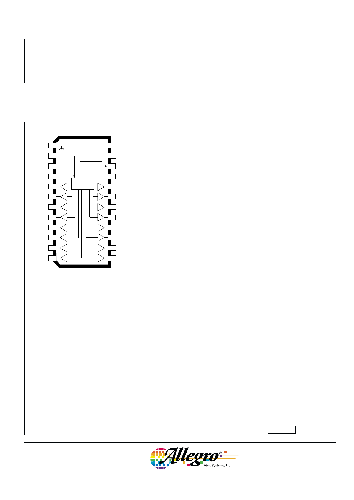
Note that the A6276EA (DIP) and the A6276ELW
(SOIC) are electrically identical and share a
common terminal number assignment.
A6276ELW
ABSOLUTE MAXIMUM RATINGS
Supply Voltage, VDD...................... 7.0 V
Output Voltage Range,
V
O
............................ -0.5 V to +17 V
Output Current, I
O
........................ 90 mA
Ground Current, I
GND
............... 1475 mA
Input Voltage Range,
V
I
.................... -0.4 V to VDD + 0.4 V
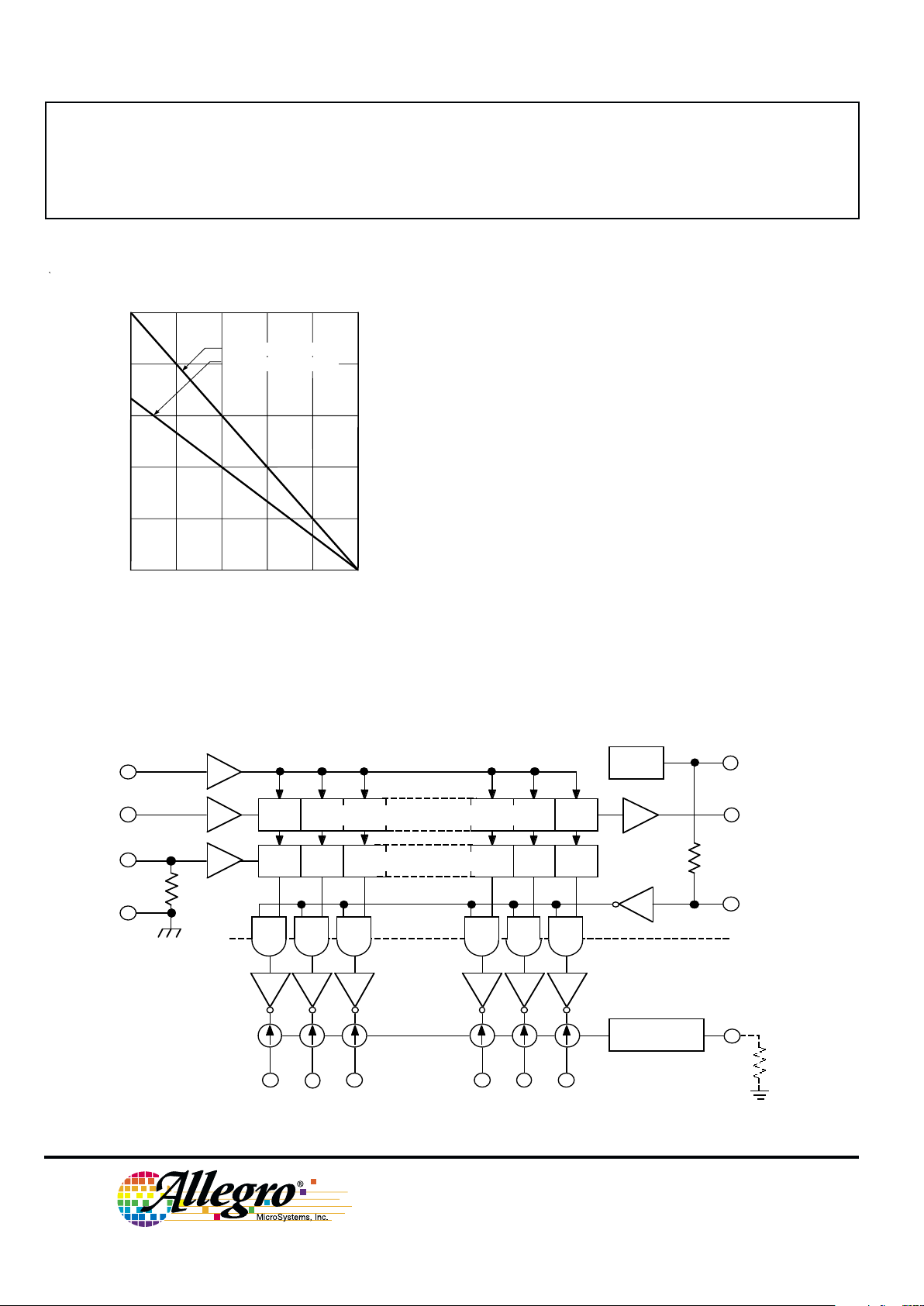
Package Power Dissipation,
P
D
..................................... See Graph
Operating Temperature Range,
T
A
............................. -40°C to +85°C
Storage Temperature Range,
T
S
........................... -55°C to +150°C
Caution: These CMOS devices have input
static protection (Class 2) but are still susceptible to damage if exposed to extremely high
static electrical charges.
FEATURES
■ To 90 mA Constant-Current Outputs
■ Under-Voltage Lockout
■ Low-Power CMOS Logic and Latches
■ High Data Input Rate
■ Functional Replacement for TB62706BN/BF
GROUND
REGISTER
LATCHES
1
2
3
817
18
19
20
21
23
4
5
6
7
22
24
SERIAL
DATA OUT
LOGIC
SUPPLY
SERIAL
DATA IN
OUTPUT
ENABLE
LATCH
ENABLE
CLOCK CK
V
DD
OE
OUT
1
OUT
2
OUT
0
OUT
12
OUT
14
OUT
13
OUT
3
OUT
15
R
EXT
I
REGULATOR
L
O
12
9
10
11
OUT
5
OUT
6
OUT
4
OUT
7
13
14
15
16
Dwg. PP-029-11
OUT
8
OUT
10
OUT
9
OUT
11
6276
16-BIT SERIAL-INPUT,
CONSTANT-CURRENT
LATCHED LED DRIVER
115 Northeast Cutoff, Box 15036
Worcester, Massachusetts 01615-0036 (508) 853-5000
2
Copyright © 2000, Allegro MicroSystems, Inc.
50 75 100 125 150
2.5
0.5
0
ALLOWABLE PACKAGE POWER DISSIPATION IN WATTS
AMBIENT TEMPERATURE IN °C
2.0
1.5
1.0
25
Dwg. GP-022-3
24-LEAD SOIC, R
θJA
= 75°C/W
24-PIN DIP, R
θJA
= 50°C/W
FUNCTIONAL BLOCK DIAGRAM
MOS
BIPOLAR
GROUND
LATCH
ENABLE
OUTPUT ENABLE
(ACTIVE LOW)
SERIAL
DATA OUT
CLOCK
SERIAL
DATA IN
SERIAL-PARALLEL SHIFT REGISTER
LATCHES
V
DD
LOGIC
SUPPLY
R
EXT
OUT0OUT
1
Dwg. FP-013-3
OUT
2
OUT
N
I
REGULATOR
O
UVLO
6276
16-BIT SERIAL-INPUT,
CONSTANT-CURRENT
LATCHED LED DRIVER
www.allegromicro.com
3
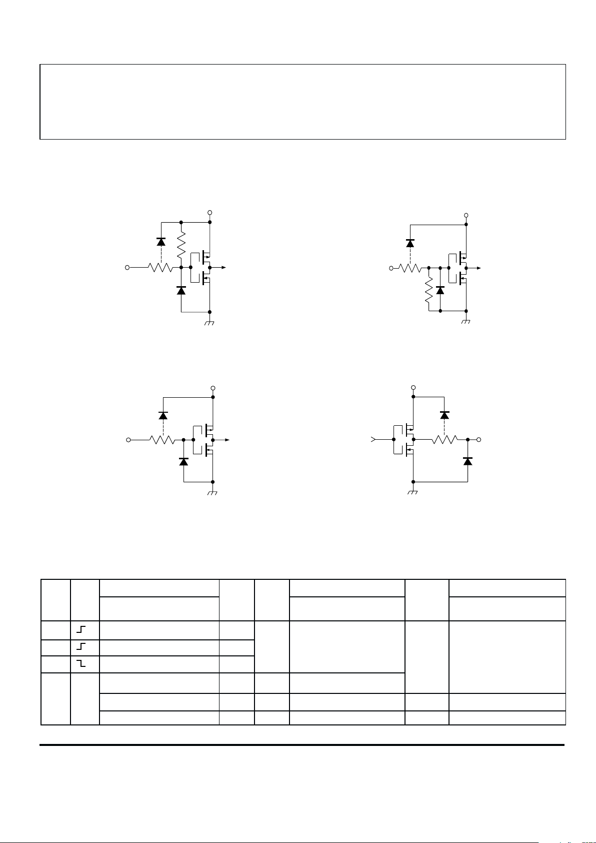
CLOCK and SERIAL DATA IN SERIAL DATA OUT
LATCH ENABLEOUTPUT ENABLE (active low)
Dwg. EP-010-6
IN
V
DD
Dwg. EP-010-7
IN
V
DD
Dwg. EP-010-5
IN
V
DD
Dwg. EP-063-1
V
DD
OUT
TRUTH TABLE
Serial Shift Register Contents Serial Latch Latch Contents Output Output Contents
Data Clock Data Enable Enable
Input Input I
1I2I3
... I
N-1IN
Output Input I1I2I3... I
N-1IN
Input I1I2I3... I
N-1
I
N
HHR
1R2
... R
N-2RN-1
R
N-1
LLR
1R2
... R
N-2RN-1
R
N-1
XR
1R2R3
... R
N-1RN
R
N
XXX...X X X L R1R2R3... R
N-1 RN
P1P2P3... P
N-1PN
P
N
HP1P2P3... P
N-1 PN
LP1P2P3... P
N-1 PN
XXX...X X H H H H ... H H
L = Low Logic (Voltage) Level H = High Logic (Voltage) Level X = Irrelevant P = Present State R = Previous State
6276
16-BIT SERIAL-INPUT,
CONSTANT-CURRENT
LATCHED LED DRIVER
115 Northeast Cutoff, Box 15036
Worcester, Massachusetts 01615-0036 (508) 853-5000
4
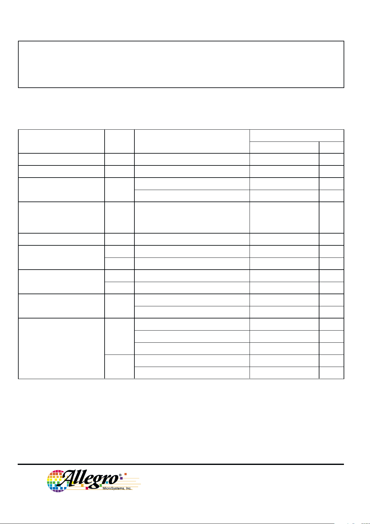
ELECTRICAL CHARACTERISTICS at TA = +25°C, VDD = 5 V (unless otherwise noted).
Limits
Characteristic Symbol Test Conditions Min. Typ. Max. Unit
Supply Voltage Range V
DD
Operating 4.5 5.0 5.5 V
Under-Voltage Lockout V
DD(UV)
VDD = 0 → 5 V 3.4 – 4.0 V
Output Current I
O
VCE = 0.7 V, R
EXT
= 250 Ω 64.2 75.5 86.8 mA
(any single output)
VCE = 0.7 V, R
EXT
= 470 Ω 34.1 40.0 45.9 mA
Output Current Matching ∆I
O
0.4 V ≤ V
CE(A)
= V
CE(B)
≤ 0.7 V:
(difference between any R
EXT
= 250 Ω – ±1.5 ±6.0 %
two outputs at same VCE)
R
EXT
= 470 Ω – ±1.5 ±6.0 %
Output Leakage Current I
CEX
VOH = 15 V – 1.0 5.0 µA
Logic Input Voltage V
IH
0.7V
DD
–VDDV
V
IL
GND – 0.3V
DD
V
SERIAL DATA OUT V
OL
IOL = 500 µA––0.4V
Voltage
V
OH
IOH = -500 µA4.6––V
Input Resistance R
I
ENABLE Input, Pull Up 150 300 600 kΩ
LATCH Input, Pull Down 100 200 400 kΩ
Supply Current I
DD(OFF)
R
EXT
= open, VOE = 5 V – 0.8 1.4 mA
R
EXT
= 470 Ω, VOE = 5 V 3.5 6.0 8.0 mA
R
EXT
= 250 Ω, VOE = 5 V 6.5 11 15 mA
I
DD(ON)
R
EXT
= 470 Ω, VOE = 0 V 7.0 13 20 mA
R
EXT
= 250 Ω, VOE = 0 V 10 22 32 mA
Typical Data is at VDD = 5 V and is for design information only.