

Allegro A6273KLW, A6273KA Datasheet
6273
Data Sheet
26180.120
ADVANCE INFORMATION
(Subject to change without notice)
January 24, 2000
LOGIC
1
CLEAR
2
IN
1
3
IN
2
OUT
4
1
OUT
5
2
6
OUT
OUT
IN
IN
GROUND
3
7
4
8
3
9
4
10
LATCHES
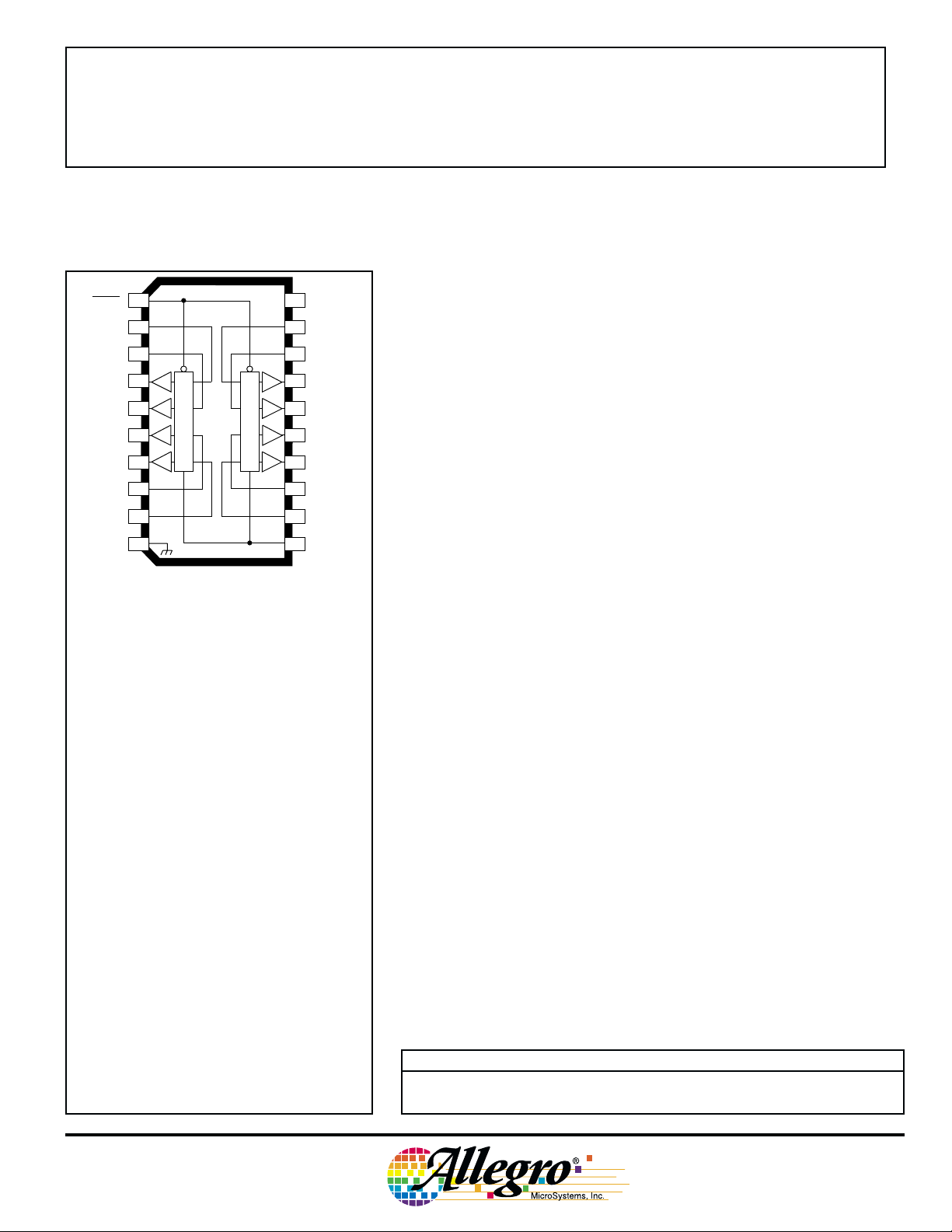
Note that the A6273KA (DIP) and the A6273KLW
(SOIC) are electrically identical and share a common terminal number assignment.
V
DD
LATCHES
20
19
18
17
16
15
14
13
12
11
SUPPLY
IN
8
IN
7
OUT
8
OUT
7
OUT
6
OUT
5
IN
6
IN
5
STROBE
Dwg. PP-015-2
8-BIT LATCHED
DMOS POWER DRIVER
The A6273KA and A6273KLW combine eight (positive-edgetriggered D-type) data latches and DMOS outputs for systems requiring
relatively high load power. Driver applications include relays, solenoids, and other medium-current or high-voltage peripheral power loads.
The CMOS inputs and latches allow direct interfacing with microprocessor-based systems. Use with TTL may require appropriate pull-up
resistors to ensure an input logic high.
The DMOS output inverts the DATA input. All of the output
drivers are disabled (the DMOS sink drivers turned OFF) with the
CLEAR input low. The A6273KA/KLW DMOS open-drain outputs are
capable of sinking up to 750 mA. Similar devices with reduced r
will be available as the A6A273.
The A6273KA is furnished in a 20-pin dual in-line plastic package.
The A6273KLW is furnished in a 20-lead wide-body, small-outline
plastic package (SOIC) with gull-wing leads for surface-mount applications. Copper lead frames, reduced supply current requirements, and
low on-state resistance allow both devices to sink 150 mA from all
outputs continuously, to ambient temperatures over 85°C.
DS(on)
ABSOLUTE MAXIMUM RATINGS
at TA = 25°C
Output Voltage, VO............................. 50 V
Output Drain Current,
Continuous, IO....................... 250 mA*
Peak, IOM.............................. 750 mA*†
Peak, IOM..................................... 2.0 A†
Single-Pulse Avalanche Energy,
EAS.............................................. 75 mJ
Logic Supply Voltage, VDD................ 7.0 V
Input Voltage Range,
VI................................. -0.3 V to +7.0 V
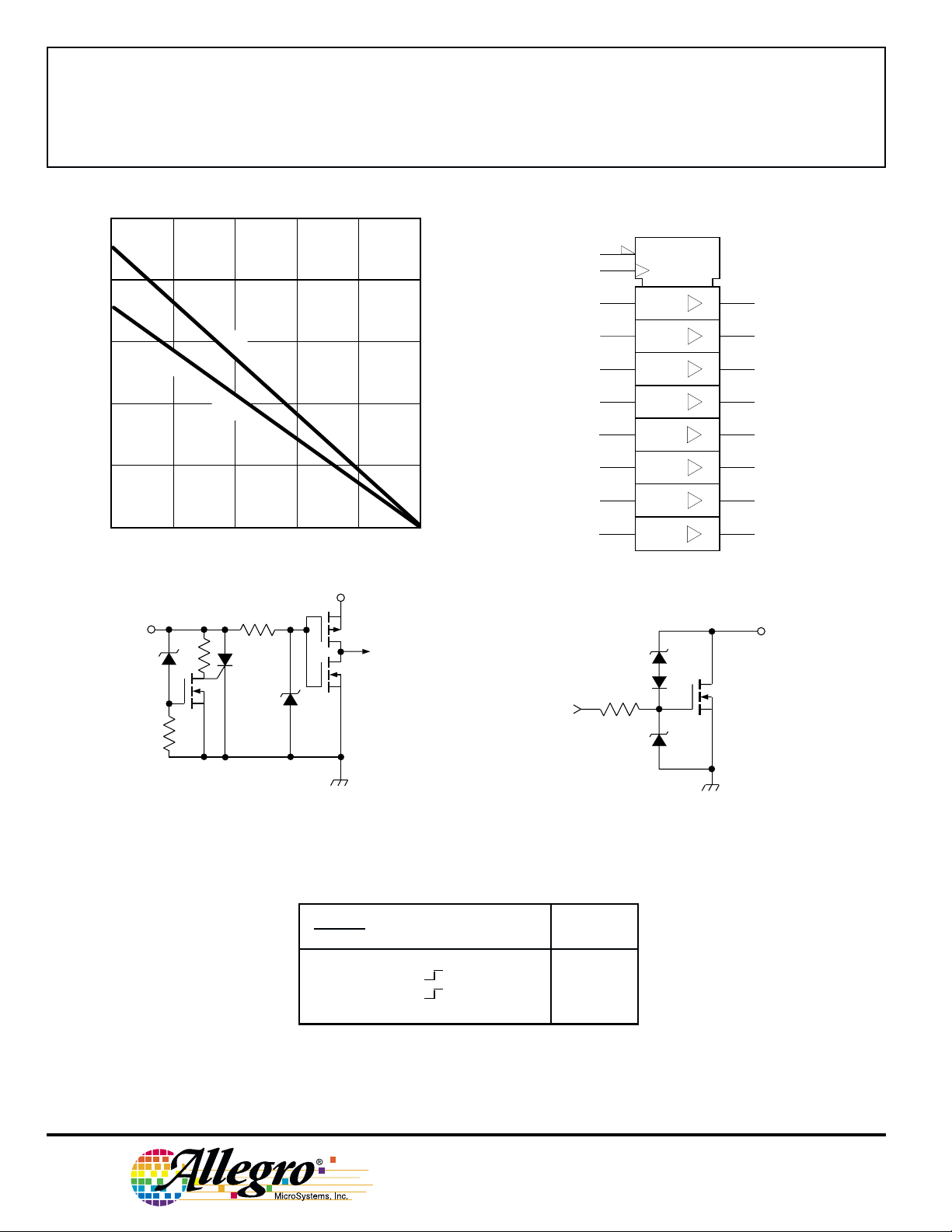
Package Power Dissipation,
PD........................................ See Graph
Operating Temperature Range,
TA.............................. -40°C to +125°C
Storage Temperature Range,
TS.............................. -55°C to +150°C
* Each output, all outputs on.
† Pulse duration ≤ 100 µs, duty cycle ≤ 2%.
Caution: These CMOS devices have input
static protection (Class 3) but are still
susceptible to damage if exposed to extremely
high static electrical charges.
FEATURES
■ 50 V Minimum Output Clamp Voltage
■ 250 mA Output Current (all outputs simultaneously)
■ 1.3 Ω Typical
■ Low Power Consumption
■ Replacements for TPIC6273N and TPIC6273DW
Always order by complete part number:
Part Number Package R
A6273KA 20-pin DIP 55°C/W 25°C/W
A6273KLW 20-lead SOIC 70°C/W 17°C/W
r
DS(on)
θJA
R
θJC
6273
g
8-BIT LATCHED
DMOS POWER DRIVER
2.5
2.0
S
U
F
F
IX
'A
', R
θJA
=
θJA
5
5
°C/W
°C
/W
Dwg. GS-004A
V
DD
1.5
1.0
0.5
0
25
ALLOWABLE PACKAGE POWER DISSIPATION IN WATTS
SUFFIX 'LW', R = 70
50 75 100 125 150
AMBIENT TEMPERATURE IN °C
IN
LOGIC SYMBOL
1
11
2
3
18
R
C1
1D 4
1D
1D8
1D9
1D12
1D13
1D
1D19
. FP-046-1
Dw
5
6
7
14
15
16
17
OUT
Dwg. EP-010-16
Dwg. EP-063
DMOS POWER DRIVER OUTPUTLOGIC INPUTS
FUNCTION TABLE
Inputs
CLEAR STROBE IN
X
LXXH
HHL
HLH
HLXR
L = Low Logic Level
H = High Logic Level
X = Irrelevant
R = Previous State
115 Northeast Cutoff, Box 15036
Worcester, Massachusetts 01615-0036 (508) 853-5000
Copyright © 2000, Allegro MicroSystems, Inc.
OUT
X
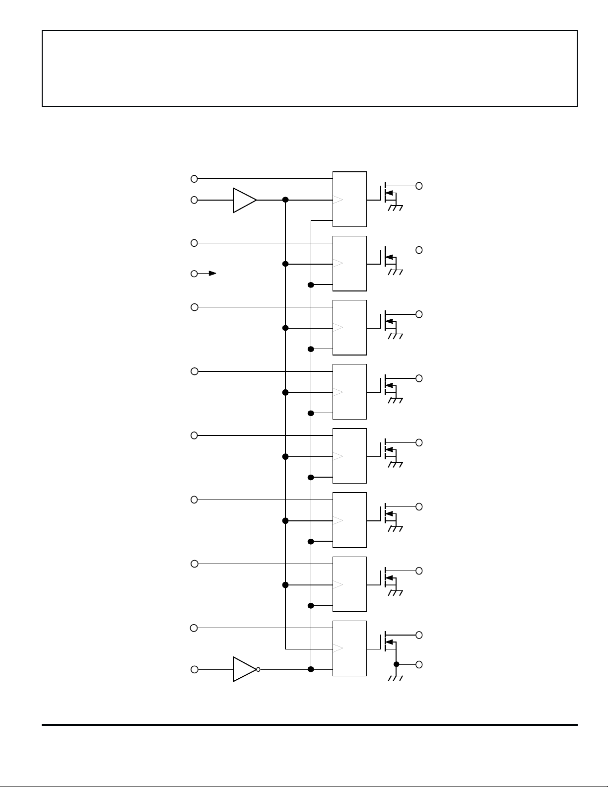
FUNCTIONAL BLOCK DIAGRAM
6273
8-BIT LATCHED
DMOS POWER DRIVER
IN
STROBE
IN
LOGIC
SUPPLY
IN
IN
IN
1
D
OUT
1
C1
CLR
2
D
OUT
2
C1
V
DD
3
CLR
D
OUT
3
C1
CLR
4
D
OUT
4
C1
CLR
5
D
OUT
5
C1
www.allegromicro.com
IN
IN
IN
CLEAR
(ACTIVE LOW)
CLR
6
D
OUT
6
C1
CLR
7
D
OUT
7
C1
CLR
8
D
OUT
8
C1
CLR
GROUND
Dwg. FP-016-2
 Loading...