

Allegro A5817SEP Datasheet
5817
ADDRESSABLE
28-LINE DECODER/DRIVER
Data Sheet
26186.20
5817
DISCONTINUED PRODUCT
Shown for Reference Only
Replaced by A6817SEP
B
OUT
OUT
OUT
OUT
OUT
OUT
OUT
OUT
OUT
GND
B0
OUTPUT ENABLE
OUT
CHIP ENABLE
6
4
5
7
B1
8
B2
9
B3
10
B4
11
B5
12
B6
13
B7
B8
B9
IC
14
15
16
17
OUTPUT DRIVER BANK B
19
20
18
IC
IC
B10
OUT
GND
3
21
B11
OUT
D
IN (MSB)
LOGIC SUPPLY
2
1
DD
V
4-TO-14 LINE DECODER
23
22
B13
B12
OUT
OUT
IN
44
24
OUT
B
C
A13
IN
43
25
OUT
A12
A
IN (LSB)
GND
424140
27
26
A11
A10
OUT
OUT
A
OUTPUT ENABLE
39
OUT
A0
38
OUT
A1
37
OUT
A2
36
OUT
A3
OUT
35
A4
34
OUT
A5
33
OUT
32
OUT
OUT
31
30
OUT
GND
29
Dwg. PP-050
A6
A7
A8
A9
OUTPUT DRIVER BANK A
28
NC
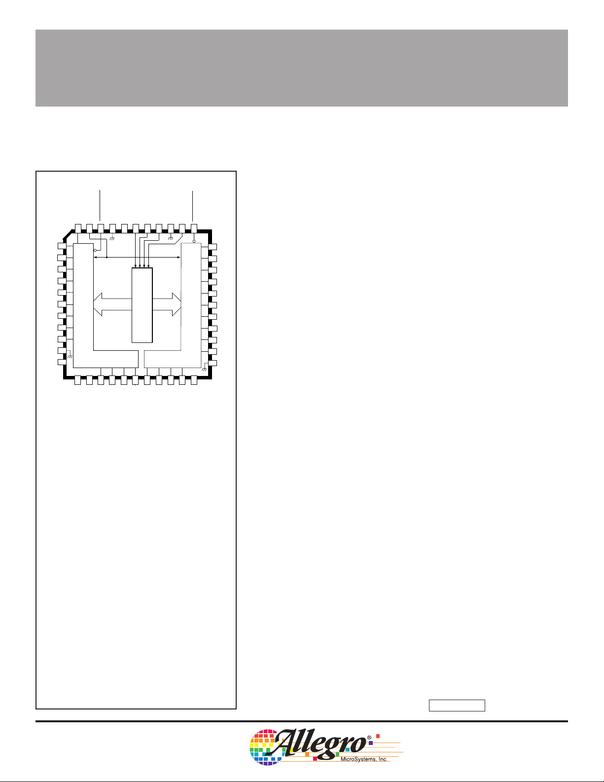
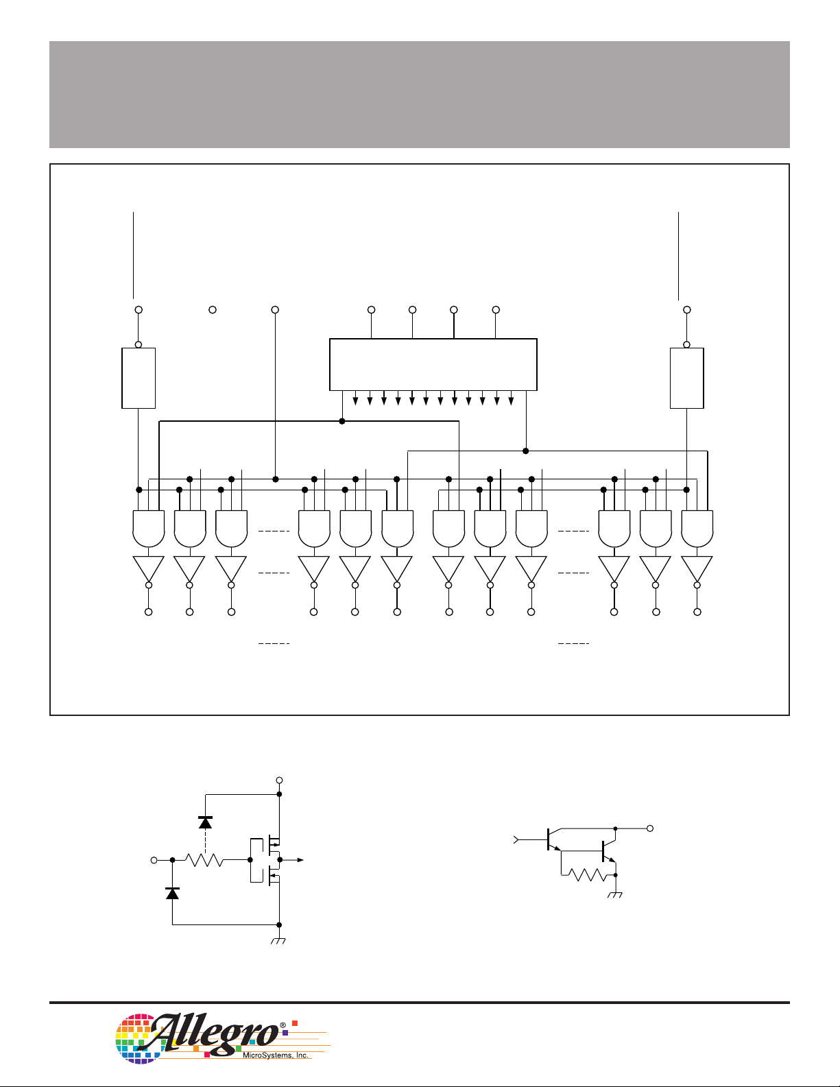
ADDRESSABLE
28-LINE DECODER/DRIVER
Intended for use in ink-jet printer applications, the A5817SEP
addressable 28-line decoder/driver combines low-power CMOS inputs
and logic with 28 high-current, high-voltage bipolar outputs. A 4-to-14
line decoder determines the selected output driver (n) in each
14-driver bank. Two independent output enable inputs (active low)
then provide the final decoding to activate 1- or 2-of-28 outputs
(OUTAn and/or OUTBn). Special internal circuitry is programmed at the
time of manufacture to adjust the output pulse timing and thereby the
energy the device delivers to the ink-jet print head.
The CMOS inputs cause minimal loading and are compatible with
standard CMOS, PMOS, and NMOS logic. Use with TTL or DTL
circuits may require appropriate pull-up resistors to ensure an input
logic high. The internal CMOS logic operates from a 5 V supply.
A CHIP ENABLE function is provided to lock out the drivers during
system power up. The 28 bipolar power outputs are open-collector
30 V Darlington drivers capable of sinking 500 mA at ambient
temperatures up to 85°C.
The A5817SEP is furnished in a 44-lead plastic chip carrier
(quad pack) for minimum-area, surface-mount applications.
ABSOLUTE MAXIMUM RATINGS
at T
= 25°C
A
Output Voltage, VCE............................. 30 V
Logic Supply Voltage, V
Input Voltage Range,
V
....................... -0.3 V to VDD + 0.3 V
IN
Output Current, I
........................... 600 mA
C
Package Power Dissipation, P
Operating Temperature Range,
T
................................. -20°C to +85°C
A
Storage Temperature Range,
T
.............................. -55°C to +150°C
S
*Derate at rate of 22 mW/°C above TA = 25°C.
Caution: CMOS devices have input static
protection but are susceptible to damage
when exposed to extremely high static
electrical charges.
.................. 7.0 V
DD
..... 2.70 W*
D
FEATURES
■ Controlled Characteristics for Ink-Jet Printers
■ Addressable Data Entry
■ 30 V Minimum V
■ CMOS, PMOS, NMOS Compatible Inputs
■ Low-Power CMOS Logic
Always order by complete part number: A5817SEP .
(BR)CEX
5817
ADDRESSABLE
28-LINE DECODER/DRIVER
FUNCTIONAL BLOCK DIAGRAM
A
B
OUTPUT ENABLE
DELAY
TURN-ON
A0
A1
OUT
OUT
LOGIC SUPPLY
OUT
CHIP ENABLE
A2
A11
OUT
B
A
IN (LSB)
IN
4-TO-14 LINE DECODER
A12
OUT
A13
OUT
OUT
IN
B0
C
D
IN (MSB)
B1
OUT
B2
OUT
B11
OUT
OUTPUT ENABLE
DELAY
TURN-ON
B12
B13
OUT
OUT
Dwg. FP-032
TYPICAL INPUT CIRCUIT TYPICAL OUTPUT DRIVER
V
DD
OUT
N
IN
Dwg. EP-021-7
Dwg. EP-010-1
115 Northeast Cutoff, Box 15036
Worcester, Massachusetts 01615-0036 (508) 853-5000
W
Copyright © 1993, Allegro MicroSystems, Inc.
 Loading...