

www.DataSheet4U.com
查询A3985供应商查询A3985供应商
A3985
Digitally Programmable
Dual Full-Bridge MOSFET Driver
Features and Benefits
▪ Serial interface for full digital control
▪ Dual full-bridge gate drive for N-channel MOSFETs
▪ Dual 6-bit DAC current reference
▪ Operation over 12 to 50 V supply voltage range
▪ Synchronous rectification
▪ Cross-conduction protection
▪ Adjustable mixed decay
▪ Fixed off-time PWM current control
▪ Low-current idle mode
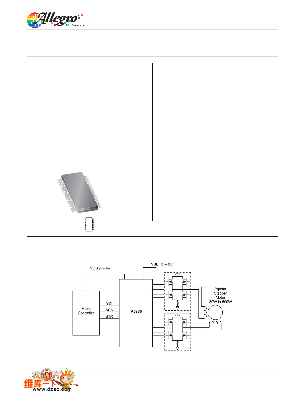
Package: 38 pin TSSOP (suffix LD)
Description
The A3985 is a flexible dual full-bridge gate driver suitable
for driving a wide range of higher power industrial bipolar 2phase stepper motors or 2-phase brushless dc motors. It can
also be used to drive two individual torque motors or solenoid
actuators. Motor power is provided by external N-channel power
MOSFETs at supply voltages from 12 to 50 V.
Full digital control is provided by two serially-accessible
registers that allow programming of off-time, blank-time,
dead-time, mixed decay ratios, synchronous rectification,
master clock source selection, and division ratio and idle
mode. All internal timings are derived from a master clock
that can be generated on-chip or provided by an external
clock such as the system clock of the master controller. A
programmable divider allows for a wide range of external
system clock frequencies.
The internal fixed off-time PWM current-control timing is
programmed via the serial interface to operate in slow, fast,
and mixed current-decay modes. The desired load-current level
and direction is set via the serial port with a direction bit and
two 6-bit linear DACs in conjunction with a reference voltage.
The seven bits of control allow maximum flexibility in torque
Approximate size
Continued on the next page…
T ypical Application
3985-DS

A3985
Digitally Programmable
Dual Full-Bridge MOSFET Driver
Description (continued)
control for a variety of step methods, from microstepping to full-step
drive. Load current in the external power MOSFET full-bridges is
set in 1.56% increments of the maximum value.
The above-supply voltage required for the high-side N-channel
MOSFETs is provided by a bootstrap capacitor. Efficiency is
enhanced by using synchronous rectification and the power FETs
are protected from shoot-through by integrated crossover-control
and programmable dead time.
In addition to crossover current control, internal circuit protection
provides thermal shutdown with hysteresis and undervoltage lockout.
Special power-up sequencing is not required. This component is
supplied in a 38-pin TSSOP (package LD) with 100% matte tin
leadframe plating.
Selection Guide
Part Number Packing*
A3985SLD-T Tube, 50 pieces per tube
A3985SLDTR-T Tape and reel, 4000 pieces per reel
*Contact Allegro for additional packing options
Absolute Maximum Ratings
Characteristic Symbol Notes Rating Units
Supply Voltage V
Logic Supply Voltage V
Logic Inputs and Outputs –0.3 to 7 V
SENSEx pins –1 to 1 V
Sxx pins –2 to 55 V
LSSx pins –2 to 5 V
GHxx pins Sxx to Sxx+15 V
GLxx pins –2 to 16 V V
Cxx pins –0.3 to Sxx+15 V
Operating Ambient Temperature T
Junction Temperature TJ(max) 150 ºC
Storage Temperature T
stg
BB
DD
A
Range S –20 to 85 ºC
–0.3 to 50 V
–0.3 to 7
–55 to 150 ºC
V
Allegro MicroSystems, Inc.
115 Northeast Cutoff, Box 15036
Worcester, Massachusetts 01615-0036 (508) 853-5000
www.allegromicro.com
2
A3985
Digitally Programmable
Dual Full-Bridge MOSFET Driver
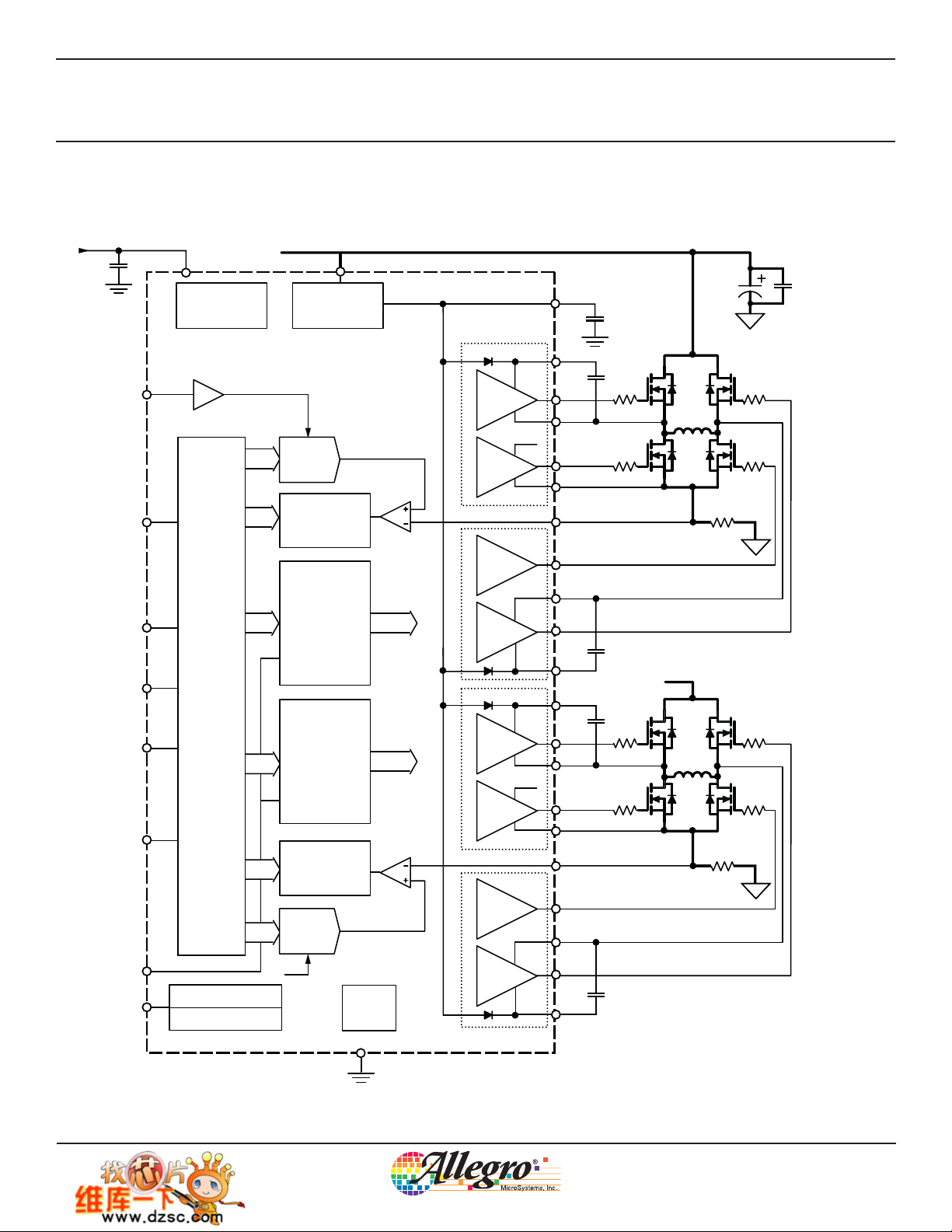
Functional Block Diagram
+5 V
REF
SDO
SDI
STR
SCK
WC
ENABLE
OSC
VDD
Bandgap Regulator
V
REF
Serial Port
Programmable Divider
Oscillator
VBB
6-bit
DAC
Programmable
PWM Timer
Blanking
Mixed Decay
Phase 1
Control Logic
Phase 2
Control Logic
Programmable
PWM Timer
Blanking
Mixed Decay
6-bit
DAC
V
REF
Phase 1
Phase 2
Protection
UVLO
TSD
Phase 1A
High-Side
Drive
Low-Side
Drive
Phase 1B
Low-Side
Drive
High-Side
Drive
Phase 2A
High-Side
Drive
Low-Side
Drive
Phase 2B
Low-Side
Drive
High-Side
Drive
V
MOTOR
VREG
CREG
C1A
CBOOT1A
GH1A
RGH1A
S1A
V
REG
GL1A
RGL1A
LSS1
SENSE1
GL1B
S1B
GH1B
CBOOT1B
C1B
C2A
CBOOT2A
GH2A
S2A
V
REG
GL2A
LSS2
SENSE2
GL2B
S2B
GH2B
CBOOT2B
C2B
V
RGH2A
RGL2A
Bridge1
RSENSE1
MOTOR
Bridge2
RSENSE2
P
RGH1B
RGL1B
P
RGH2B
RGL2B
P
GND
Allegro MicroSystems, Inc.
115 Northeast Cutoff, Box 15036
Worcester, Massachusetts 01615-0036 (508) 853-5000
www.allegromicro.com
3

A3985
Digitally Programmable
Dual Full-Bridge MOSFET Driver
ELECTRICAL CHARACTERISTICS at T
Characteristics Symbol Test Conditions Min. Typ. Max. Units
Supply and Reference
Load Supply Voltage Range V
Load Supply Current I
Load Supply Idle Current I
Logic Supply Voltage Range V
Logic Supply Current I
Logic Supply Idle Current I
Regulator Output V
Bootstrap Diode Forward Voltage V
Gate Output Drive
Turn-On Rise Time t
Turn-Off Fall Time t
Turn-On Propagation Delay t
Turn-Off Propagation Delay t
Crossover Dead Time t
Pull-Up On Resistance R
Pull-Down On Resistance R
Short-Circuit Current – Source
1
Short-Circuit Current – Sink I
DEAD
DS(on)UPIGH
DS(on)DNIGL
I
SC(source)
SC(sink)
GHx Output Voltage V
GLx Output Voltage V
Logic Inputs
Input Low Voltage V
Input High Voltage V
Input Hysteresis V
Input Current
1
Output Low Voltage V
Output High Voltage V
Output Leakage current
1
I
Oleak
= 25°C, VDD = 5 V, VBB = 12 to 50 V, unless noted otherwise
A
BB
f
BB
BBQ
DD
DD
DDQ
REGIREGInt
fBOOTIfBOOT
p(on)
p(off)
MCK
ENABLE = High, outputs disabled – – 6 mA
Word1:Bit D18 = 0 – – 100 μA
Word1:Bit D18 = 0 – – 300 μA
C
r
f
C
LOAD
LOAD
ENABLE low to gate drive on – 120 – ns
ENABLE high to gate drive off – 120 – ns
f
MCK
Word1:Bits D1 and D2 = 00
= 4 MHz, C
= 1000 pF – – 10 mA
LOAD
= 30 mA 11.25 – 13 V
= 10 mA 0.6 0.8 1 V
= 1000 pF, 20% to 80% 80 120 160 ns
= 1000 pF, 80% to 20% 40 60 80 ns
= 4 MHz,
12 – 50 V
3.0 – 5.5 V
– – 10 mA
0.5 – 0.75 μs
= –25 mA 30 40 55 Ω
= 25 mA 14 19 24 Ω
–140 –110 –80 mA
160 200 250 mA
GHx
GLx
IL
IH
IHys
I
IN
OL
OH
CBOOTx fully charged V
SDO, IOL= 0.5 mA
SDO, IOH= –0.3 mA
SDO, STR = 1, 0 V< VO< V
DD
– 0.2 – – V
C
V
REG
0.2
– – 0.3 V
0.7 V
150 300 – mV
–1 – 1 μA
V
DD
0.5
–1
–
DD
–
––V
V
DD
––V
0.5 V
V
1 μA
Continued on the next page...
Allegro MicroSystems, Inc.
115 Northeast Cutoff, Box 15036
Worcester, Massachusetts 01615-0036 (508) 853-5000
www.allegromicro.com
4
A3985
Digitally Programmable
Dual Full-Bridge MOSFET Driver
ELECTRICAL CHARACTERISTICS, continued, at T
Characteristics Symbol Test Conditions Min. Typ. Max. Units
Current Control
f
Blank Time t
Fixed Off-Time t
BLANK
OFF
MCK
Word1:Bits D1 and D2 = 00
f
MCK
Word1:Bits D3 to D7 = 01010, and
D15 = 0
Reference Input Voltage V
Internal Reference Voltage V
Current Trip Point Error
Reference Input Current
2
1
Internal Oscillator Frequency f
Maximum Clock Input Frequency f
Master Clock Frequency f
REF
REFInt
E
ITrip
I
REF
OSC
EXTmax
MCK
20 kΩ to V
V
REF
R
OSC
External clock selected – 10 – MHz
Protection
VREG Undervoltage Lockout V
VREG Undervoltage Lockout
Hysteresis
V
REGUVHys
VDD Undervoltage Lockout V
VDD Undervoltage Lockout
Hysteresis
V
DDUVHys
Overtemperature Shut Down T
Overtemperature Shut Down
Hysteresis
T
REGUV
DDUV
TSD
TSDHys
Decreasing V
Decreasing V
Temperature increasing – 165 – ºC
Recovery = T
= 25°C, VDD = 5 V, VBB = 12 to 50 V, unless noted otherwise
A
= 4 MHz;
–1–μs
= 4 MHz,
21.75 – 22 μs
0.8 – 2 V
DD
1.9 2.0 2.1 V
= 2 V – – ±5 %
–3 0 3 μA
= 10 kΩ 3.2 4 4.8 MHz
0.5 4 5 MHz
REG
7.5 8 8.5 V
100 200 – mV
DD
2.45 2.7 2.95 V
50 100 – mV
TSD
– T
TSDHys
–15–ºC
Continued on the next page...
THERMAL CHARACTERISTICS
Characteristic Symbol Test Conditions* Value Units
Package Thermal Resistance R
*Additional thermal information available on Allegro Web site.
θJA
4-layer PCB, based on JEDEC standard 47 ºC/W
1-layer PCB with copper limited to solder pads 114 ºC/W
Allegro MicroSystems, Inc.
115 Northeast Cutoff, Box 15036
Worcester, Massachusetts 01615-0036 (508) 853-5000
www.allegromicro.com
5

A3985
Digitally Programmable
Dual Full-Bridge MOSFET Driver
ELECTRICAL CHARACTERISTICS, continued, at T
= 25°C, VDD = 5 V, VBB = 12 to 50 V, unless noted otherwise
A
Characteristics Symbol Test Conditions Min. Typ. Max. Units
Serial Data Timing
Serial Clock High Time t
Serial Clock Low Time t
Strobe Lead Time t
Strobe Lag Time t
Strobe High Time t
Data Out Enable Time t
Data Out Disable Time t
Data Out Valid Time from SCK Falling t
Data Out Hold Time from SCK Falling t
Data In Set-up Time to SCK Rising t
Data In Hold Time from SCK Rising t
WC Set-up Time to STR Rising t
WC Hold Time from STR Rising t
WC Hold Time from STR Falling t
1
For input and output current specifications, negative current is defined as coming out of (sourcing) the specified device pin.
2
Current Trip Point Error is the difference between actual current trip point and the target current trip point, referred to full
scale (100%) current: E
= 100 × (I
ITrip
SCKH
SCKL
STLD
STLG
STRH
SDOE
SDOD
SDOV
SDOH
SDIS
SDIH
SWCS
SWCH
SLWCH
TripActual
– I
TripTarget
) / I
FullScale %
50
50
30
30
150
––
––
––
––
––
––
––
––
5
15
10
15
50
30
––
––
––
––
––
––
40
30
40
Serial Data Timing Diagram
ns
ns
ns
ns
ns
ns
ns
ns
ns
ns
ns
ns
ns
ns
WC
STR
SCK
SDI
SDO
t
SDOE
t
STLD
t
SDIS
D18
t
SDOV
**
Dx = Current data transfer block
Dx
= Previous data transfer block
*
= Undefined, usually LSB from previous transfer
**
D18
t
STRH
t
SWCH
6
t
SLWCH
t
SCKH
t
SDIH
t
SDOH
*
t
SCKL
D17 D0
D17
*
t
SWCS
t
STLG
t
SDOD
D0
*
Allegro MicroSystems, Inc.
115 Northeast Cutoff, Box 15036
Worcester, Massachusetts 01615-0036 (508) 853-5000
www.allegromicro.com

A3985
Digitally Programmable
Dual Full-Bridge MOSFET Driver
Functional Description
Basic Operation
The A3985 is a highly-configurable dual full-bridge FET
driver with built-in digital current control. All features are
accessed through a simple SPI (Serial Peripheral Interface)
compatible serial port, allowing multiple motors to be controlled with as few as three wires.
Because the full-bridge control circuits are independently
controlled, the A3985 can be used to drive 2-phase bipolar
stepper motors and 2-phase brushless dc (BLDC) motors.
The current in each of the two external power full-bridges
(which are all N-channel MOSFETs) is regulated by a fixed
off-time PWM control circuit. The full-bridge current at each
step is set by the value of an external current sense resistor,
R
voltage, V
, in the ground connection to the bridge, a reference
SENSEX
, and the output of the DAC controlled by the
REF
serial data.
The use of PWM with N-channel MOSFETs provides the
most cost-effective solution for a high efficiency motor drive.
The A3985 provides all the necessary circuits to ensure
that the gate-source voltage of both high-side and low-side
external MOSFETs are above 10 V, and that there is no crossconduction (shoot through) in the external bridge. Specific
functions are described more fully in the following sections.
Power Supplies
To limit the voltage drop when the charge current is provided, this pin should be decoupled with a ceramic capacitor, CREG, to ground. The value C
should typically
REG
be 40 times the value of the bootstrap capacitor for PWM
frequencies up to 14 kHz. Above 14 kHz, the minimum
recommended value can be determined from the following
formula:
C
> C
REG
where C
REG
and C
BOOT
PWM frequency, in kHz. V
× 3 × f
BOOT
are in nF, and f
is monitored, and if the volt-
REG
PWM
,
PWM
is the maximum
age becomes too low, the outputs will be disabled.
REF The reference voltage, V
, at this pin sets the
REF
maximum (100%) peak current. The REF input is internally
limited to 2 V when a 20 kΩ pull-up resistor is connected
between VREF and VDD. This allows the maximum refer-
ence voltage to be set without the need for an externallygenerated voltage. An external reference voltage below the
maximum can also be input on this pin. The voltage at VREF
is divided by the range select ratio Gm to produce the DAC
reference voltage level.
OSC The PWM timing is based on a master clock, typically
running at 4 MHz. The master clock period is used to derive
the PWM off-time, dead time, and blanking time.
Two power connections are required. The motor power supply should be connected to VBB to provide the gate drive
levels. Power for internal logic is provided by the VDD
input. Internal logic is designed to operate from 3 to 5.5 V,
allowing the use of 3.3 or 5 V external logic interface circuits.
GND The ground pin is a reference voltage for internal logic
and analog circuits. There is no large current flow through
this pin. To avoid any noise from switching circuits, this
should have an independent trace to the supply ground star
point.
VREG The voltage at this pin is generated by a low-drop-out
linear regulator from the VBB supply. It is used to oper-
ate the low-side gate drive outputs, GLxx, and to provide
the charging current for the bootstrap capacitors, CBOOTx.
The master clock frequency can be set by an internal oscillator or by one of three division ratios of an external clock.
These four options are selected by bits D12 and D13 of the
Control register word.
When the A3985 is configured to use an external clock,
this is input on the OSC pin and will usually provide more
precision than using the internal oscillator. The three internal
divider alternatives provide flexibility in setting the master
clock frequency based on available external system clocks.
If internal timing is selected, f
is configured by using
OSC
an external resistor, ROSC, connected from the OSC pin to
GND. This sets the frequency (in MHz) to approximately:
f
where R
≈ 100 / (6 + 1.9 × R
OSC
, in kΩ, is typically between 50 kΩ and 10 kΩ.
OSC
Allegro MicroSystems, Inc.
115 Northeast Cutoff, Box 15036
Worcester, Massachusetts 01615-0036 (508) 853-5000
www.allegromicro.com
OSC
) ,
7

A3985
Digitally Programmable
Dual Full-Bridge MOSFET Driver
SDI, SCK, STR, SDO These are the serial port interface
pins. Data is clocked into SDI by a clock signal on SCK.
The data is then latched by a signal on STR. If required, the
serial data out pin, SDO, can be used to read back the previously-latched serial data or to form a daisy chain for multiple
controllers using a single STR connection. (For bit assignment details, see the Bit Assignments table.)
WC This input provides a lockout capability for writing
to the Control register. When set to logic high, no changes
can be made to the Control register through the serial port.
When at logic low, the data on the serial port will update the
Control register (if selected by D0 = 1) while STR is high.
This provides a mechanism to avoid inadvertently changing
the Control register settings by erroneous or corrupt serial
data signals.
Gate Drive
The A3985 is designed to drive external power N-channel MOSFETs. It supplies the transient currents necessary
to quickly charge and discharge the external FET gate
capacitance in order to reduce dissipation in the external
FET during switching. The charge and discharge rate can
be controlled using an external resistor, RGx, in series with
the connection to the gate of the FET. Cross-conduction is
prevented by the gate drive circuits which introduce a dead
time, t
mentary FET on. t
master clock, depending on the corresponding value set in
the Control register (Word 1: bits D1 and D2). t
up to 1 cycle longer than the programmed value, to allow
synchronization with the master clock.
ENABLE This input simply turns off all of the power MOS-
FETs. Set to logic high to disable outputs. When at logic low,
the internal control enables the outputs as required. Inputs to
the registers and the internal sequencing logic are all active
independent of the ENABLE input state.
, between switching one FET off and the comple-
DEAD
is at least 2, 3, 4, or 6 periods of the
DEAD
DEAD
can be
is low. When the output swings high, the voltage on this terminal rises with the output to provide the boosted gate voltage needed for the high-side N-channel power MOSFETs.
The bootstrap capacitor should be ceramic and have a value
of 10 to 20 times the total MOSFET gate capacitance.
GH1A, GH1B, GH2A, and GH2B High-side gate drive
outputs for external N-channel MOSFETs. External series
gate resistors can be used to control the slew rate seen at
the gate, thereby controlling the di/dt and dv/dt at the motor
terminals. GHxx = 1 (high) means that the upper half of the
driver is turned on and will source current to the gate of the
high-side MOSFET in the external motor-driving bridge.
GHxx =
turned on and will sink current from the external MOSFET
gate circuit to the respective Sxx pin.
S1A, S1B, S2A, and S2B Directly connected to the
motor, these terminals sense the voltages switched across the
load and define the negative supply for the floating high-side
drivers. The discharge current from the high-side MOSFET
gate capacitance flows through these connections which
should have low impedance traces to the MOSFET bridge.
GL1A, GL1B, GL2A, and GL2B Low-side gate drive
outputs for external N-channel MOSFETs. External series
gate resistors (as close as possible to the MOSFET gate)
can be used to reduce the slew rate seen at the gate, thereby
controlling the di/dt and dv/dt at the motor terminals.
GLxx = 1 (high) means that the upper half of the driver is
turned on and will source current to the gate of the low-side
MOSFET in the external motor-driving bridge. GLxx = 0
(low) means that the lower half of the driver is turned on and
will sink current from the gate of the external MOSFET to
the LSSx pin.
LSS1 and LSS2 Low-side return path for discharge of the
gate capacitors, connected to the common sources of the
low-side external FETs through low-impedance traces.
0 (low) means that the lower half of the driver is
Internal PWM Current Control
C1A, C1B, C2A, and C2B High-side connections for the
bootstrap capacitors, CBOOTx, and positive supply for high-
side gate drivers. The bootstrap capacitors are charged to
approximately V
when the associated output Sxx terminal
REG
Each full-bridge is independently controlled by a fixed offtime PWM current control circuit that limits the load current
in the phase to a desired value, I
of source and sink MOSFETs are enabled and current flows
Allegro MicroSystems, Inc.
115 Northeast Cutoff, Box 15036
Worcester, Massachusetts 01615-0036 (508) 853-5000
www.allegromicro.com
. Initially, a diagonal pair
Trip
8

A3985
Digitally Programmable
Dual Full-Bridge MOSFET Driver
through the motor winding and the current sense resistor,
RSENSEx. When the voltage across RSENSEx equals the
DAC output voltage, the current sense comparator resets
the PWM latch, which turns off the source MOSFET (slow
decay mode) or the sink and source MOSFETs (fast decay
mode). The maximum value of current limiting is set by the
selection of R
and the voltage at the REF input, with a
SENSE
transconductance function approximated by:
where G
I
Trip(max)
is the range factor defined by in the Data register
m
= V
/ (Gm × R
REF
SENSE
) ,
(Word0: Bits D17 and D18).
The DAC output reduces the VREF output to the current
sense comparator, V
V
DAC
, in precise steps:
DAC
= [(1 + DAC) × V
REF
] / 64 ,
where DAC is the decimal equivalent value of the Bridge
DAC bits in the Data register (Word0: Bits D1 through D6
for Bridge 1, Bits 9 through 14 for Bridge 2). (Active codes
are represented by the values 1 through 63. Programming a
DAC input code to 0 disables the corresponding bridge, and
results in minimum load current.)
The current trip level for each DAC value then becomes:
I
TripDAC
= V
DAC
/ (Gm × R
SENSE
) .
PWM Timer Function All bridge control timing is based
on the master clock. The PWM timer is programmed via the
serial port to provide fixed off-time PWM signals to the control block. The off-time, t
the Off-Time bits in the Control register (Word1, Bits D3
through D7) using the serial port. t
longer than the programmed value, to synchronize with the
master clock.
Blanking When a source driver is turned on, a current
spike occurs due to the reverse-recovery currents of the
clamp diodes and switching transients related to distributed
capacitance in the load. To prevent false overcurrent detection due to this current spike, the output from the current
sense comparator is ignored (blanked) for a duration of time
called the blank time. The blank timer runs, when a source
power MOSFET is turned on, to provide the programmable
, is selected by programming
OFF
may be up to 1 cycle
OFF
blanking function The blank timer is reset when PHASE is
changed.
The blank time can be set to 4, 6, 8, or 12 periods of the master clock by programming the blank time bits in the Control
register (Word1, Bits D1 and D2) using the serial port.
Dead Time To prevent cross-conduction (shoot through)
in the power full-bridge, a dead time, t
between switching one MOSFET off and switching the
complementary MOSFET on. The dead time, t
nominally half of t
but may be up to 1 cycle longer to
BLANK ,
synchronize with the master clock.
, is introduced
DEAD
DEAD
, is
Mixed Decay Operation
Mixed decay is a technique that provides greater control
of phase currents while the current is decreasing. When a
stepper motor is driven at high speed, the back EMF from
the motor will lag behind the driving current. If a passive
current decay mode, such as slow decay, is used in the current control scheme, then the motor back EMF can cause the
phase current to rise out of control. Mixed decay eliminates
this effect by putting the full-bridge initially into fast decay,
and then switching to slow decay after some time. Because
fast decay is an active (driven) decay mode, this portion of
the current decay cycle will ensure that the current remains
in control. Using fast decay for the full current decay time
(off-time, t
switching to slow decay once the current is in control will
reduce the ripple current value. The portion of the off-time
that the full-bridge has to remain in fast decay will depend
on the characteristics and the speed of the motor.
When the phase current is rising, the motor back EMF does
not affect the current control, and slow decay may be used
to minimize the phase current ripple. The A3985 must be
programmed to switch between slow decay, when the current is rising, and mixed decay, when the current is falling.
To simplify this programming sequence the decay mode is
included in the data word (Word0) with the phase current trip
level and the phase current direction.
When mixed decay is used, the portion of the off-time that
the full-bridge remains in fast decay, t
) would result in a large ripple current, but
OFF
, is selected by pro-
FD
Allegro MicroSystems, Inc.
115 Northeast Cutoff, Box 15036
Worcester, Massachusetts 01615-0036 (508) 853-5000
www.allegromicro.com
9

A3985
Digitally Programmable
Dual Full-Bridge MOSFET Driver
gramming the Fast Decay Time bits in the Control register
(Word1, Bits D8 through D11). If tFD is set longer than t
the device effectively operates in full fast decay mode.
Selecting between slow decay and mixed decay is done by
programming the Mode bits in the Data register (Word0, Bits
D8 and D16) using the serial port.
OFF
,
Synchronous Rectification When a PWM off-cycle
is triggered, load current recirculates according to the decay
mode selected by the control logic. The synchronous rectification feature turns on the appropriate MOSFETs during the
current decay and effectively shorts out the body diodes with
the low R
sipation significantly and eliminates the need for additional
Schottky diodes.
Synchronous rectification can be set to one of three distinct
modes by programming the Synchronous Rectification bits
in the Control register (Word1, Bits D14 through D15) using
the serial port. The modes are:
• Active This mode prevents reversal of the load current by
turning off synchronous rectification when a zero current
level is detected. This prevents the motor winding from
conducting in the reverse direction.
• Passive This mode allows reversal of current, but will
turn of the synchronous rectifier circuit if the load current
inversion ramps up to the current limit, I
• Disabled During this mode, MOSFET switching does not
occur during load recirculation. Usually, this setting would
only be used with 4 additional external clamp diodes per
bridge.
of the MOSFET. This lowers power dis-
DS(ON)
TripDAC
.
Shutdown Operation In the event of an overtempera-
ture fault, or an undervoltage fault on VREG, the gate drive
outputs are disabled until the fault condition is removed.
At power-up, and in the event of low voltage at VDD, the
under voltage lockout (UVLO) circuit disables the gate drive
outputs until the voltage at VDD reaches the minimum level.
Once VDD is above the minimum level, the data in the serial
port is reset to all 0s, ensuring a safe power-up condition.
be used to connect several A3985s in a serial daisy chain.
The programmable functions allow maximum flexibility in
configuring the PWM to the motor drive requirements. The
serial data is written as two 19-bit words: 18 bits of data plus
1 bit to select the destination register.
Serial Port Write Timing Operation The serial port tim-
ing requirements are specified in the electrical characteristics
table, and illustrated in the Serial Data Timing diagram.
Data is received on the SDI pin and clocked through a shift
register on the rising edge of the clock signal received on the
SCK pin. STR is normally held high, and is only brought low
to initiate a write cycle. No data is clocked through the shift
register when STR is high.
The 18 data bits for a register are input MSB first, followed by the register select bit, D0. After D0 is clocked
into the shift register, STR goes high to latch the data into
the selected register. When this occurs, the internal control
circuits immediately act on the new data.
The Control register can only be written if the WC pin is at
logic low. If WC is high and D0 = 1 (indicating the Control
register), the data will be ignored on the rising edge of STR.
The state of the WC pin does not affect writing to the Data
register, and the pin can be tied to GND when Control register protection is not required.
Note that the number of bits clocked through the shift register is irrelevant and only the last 19 bits before STR goes
high will be latched. This allows several A3985 devices to be
daisy-chained and updated together with a single STR rising
edge.
Data Register (Word 0) Bit Assignments
This section describes the function of the individual bit
values in the Data register, one of the two registers accessed
through the serial port. The assignments are summarized in
the Bit Assignments table.
Serial Interface
The A3985 is controlled by a 3-wire serial port using data,
clock and strobe inputs on the SDI, SCK and STR pins
respectively. An additional serial data output on SDO can
D0 – Register Select Indicates which register should
receive the data. For the Data register, this is set to 0.
D1 through D6 – Bridge 1 Linear DAC These six bits
set the desired current level for Bridge 1. Setting all six bits
Allegro MicroSystems, Inc.
115 Northeast Cutoff, Box 15036
Worcester, Massachusetts 01615-0036 (508) 853-5000
www.allegromicro.com
10

A3985
Digitally Programmable
Dual Full-Bridge MOSFET Driver
to 0 disables Bridge 1, with all drivers off (see Internal PWM
Current Control, in the Functional Description section).
D7 – Bridge 1 Phase Controls the direction of output cur-
rent for Bridge (load) 1.
D7 S1A S1B
0LH
1HL
D8 – Bridge 1 Mode Determines whether slow decay is
forced or mixed decay, according to Word 1 Bits D3 to D11,
is allowed.
D8 Mode
0 Mixed-decay
1 Slow-decay
D9 – D14 Bridge 2 Linear DAC These six bits set the
desired current level for Bridge 2. Setting all six bits to 0
disables Bridge 2, with all drivers off (see Internal PWM
Current Control, in the Functional Description section).
D15 – Bridge 2 Phase Controls the direction of output
current for Bridge (load) 2.
D15 S2A S2B
0LH
1HL
D16 – Bridge 2 Mode Determines whether slow decay is
forced or mixed decay, according to Word 1 Bits D3 to D11,
is allowed.
D16 Mode
0 Mixed-decay
1 Slow-decay
D17 and D18 – Gm Range Select These bits determine
the range scaling factor, Gm , used in PWM current control,
according to the following formula:
I
TripDAC
= V
DAC
/ (Gm × R
SENSEx
)
Control Register (Word 1) Bit Assignments
This section describes the function of the individual bit val-
ues in the Control register, one of the two registers accessed
through the serial port. The assignments are summarized in
the Bit Assignments table.
Note that the Control register can only be updated when the
WC pin is logic low.
D0 – Register Select Indicates which register should
receive the data. For the Control register, this is set to 1.
D1 and D2 – Blank Time These two bits set the value of
the scaling factor, α / f
the current-sense comparator. The factor for t
because t
= t
DEAD
BLANK
D2 D1 t
00
0 1 6 / f
1 0 8 / f
1 1 12 / f
, used for determining t
MCK
/ 2 .
BLANK
4 / f
MCK
MCK
MCK
MCK
(t
BLANK
2 / f
3 / f
4 / f
6 / f
t
DEAD
DEAD
/ 2)
MCK
MCK
MCK
MCK
for
BLANK
also is set,
D3 through D7 – Fixed Off Time These five bits set the
fixed off-time for the internal PWM control circuitry. Fixed
off-time is defined by:
t
= [(1 + n) × (8 / f
OFF
MCK
)] – 1 / f
MCK
,
where n = 0 to 31.
For example, with a master clock frequency of 4 MHz, the
fast-decay time would be adjustable within the range
1.75 to 63.75 μs, in increments of 2 μs.
D8 through D11 – Fast Decay Time These four bits set
the fast decay portion of fixed off-time for the internal PWM
control circuitry. The fast-decay portion is defined by:
D18 D17 G
00 8
01 12
10 16
11 20
m
tFD = [(1 + n) × 8 / f
MCK
)] – 1 / f
MCK
,
where n = 0 to 15.
For example, with a master clock frequency of 4 MHz, the
fast decay time would be adjustable within the range
1.75 to 32.75 μs, in increments of 2 μs.
Allegro MicroSystems, Inc.
115 Northeast Cutoff, Box 15036
Worcester, Massachusetts 01615-0036 (508) 853-5000
www.allegromicro.com
11

A3985
Digitally Programmable
Dual Full-Bridge MOSFET Driver
Note that, for tFD > t
full fast-decay mode.
D12 and D13 – Master Clock Control An internal
oscillator can be used for the timing functions, and if more
precise control is required, an external clock can be input to
the OSC terminal (for configuration information, refer to the
Functional Description section). To accommodate a wider
range of external system clocks, an internal divider is provided to generate the desired master clock frequency, f
according to the following table:
D13 D12 Master Clock Source and f
0 0 Internal oscillator*
0 1 External clock rate
1 0 External clock rate / 2
1 1 External clock rate / 4
*4 MHz typical, configurable with external resistor, ROSC.
, the device effectively operates in
OFF
MCK
MCK
D14 and D15 – Synchronous Rectification Two bits
are used to set the mode for sunchronous rectification. The
modes are described in the synchronous rectification section
of the Functional Description section.
D15 D14
0 0 Disabled
,
0 1 Disabled
1 0 Active
1 1 Passive
Synchronous
Rectification Mode
D16 and D17 – Reserved These bits are reserved for test-
ing and should be programmed to 0 during normal operation.
D18 – Idle Mode The device can be placed in a low power
mode by writing a 0 to D18. This disables the outputs and
the device draws a lower load supply current. The undervoltage monitor circuit remains active. When leaving idle mode,
D18 should be set to 1 for 1 ms before attempting to enable
any output driver.
Bit Assignments Table
Data Register Control Register
Word Bit Function Word Bit Function
D0 Register Select = 0
D1 Bridge 1, DAC bit 0 (LSB) D1 Blank-time bit 0 (LSB)
D2 Bridge 1, DAC bit 1 D2 Blank-time bit 1 (MSB)
D3 Bridge 1, DAC bit 2 D3 Off-time bit 0 (LSB)
D4 Bridge 1, DAC bit 3 D4 Off-time bit 1
D5 Bridge 1, DAC bit 4 D5 Off-time bit 2
D6 Bridge 1, DAC bit 5 (MSB) D6 Off-time bit 3
D7 Bridge 1, Phase D7 Off-time bit 4 (MSB)
D8 Bridge 1, Mode D8 Fast-decay time bit 0 (LSB)
0
D9 Bridge 2, DAC bit 0 (LSB) D9 Fast-decay time bit 1
D10 Bridge 2, DAC bit 1 D10 Fast-decay time bit 2
D11 Bridge 2, DAC bit 2 D11 Fast-decay time bit 3 (MSB)
D12 Bridge 2, DAC bit 3 D12 Master Clock Control bit 0 (LSB)
D13 Bridge 2, DAC bit 4 D13 Master Clock Control bit 1 (MSB)
D14 Bridge 2, DAC bit 5 (MSB) D14 Synchronous Rectification Control bit 0 (LSB)
D15 Bridge 2, Phase D15 Synchronous Rectification Control bit 1 (MSB)
D16 Bridge 2, Mode D16 Reserved
D17 Range Select bit 0 D17 Reserved
D18 Range Select bit 1 D18 Idle Mode
1
D0 Register Select = 1
Allegro MicroSystems, Inc.
115 Northeast Cutoff, Box 15036
Worcester, Massachusetts 01615-0036 (508) 853-5000
www.allegromicro.com
12

A3985
Digitally Programmable
Dual Full-Bridge MOSFET Driver
Applications Information
Current Sensing
To minimize inaccuracies in sensing the I
level caused by ground-trace IR drops, the sense resistor,
RSENSEx, should have an independent return to the supply
ground star point. For low-value sense resistors, the IR drops
in the sense resistor PCB traces can be significant and should
be taken into account. The use of sockets should be avoided
as they can introduce variation in RENSE
contact resistance.
current
PEAK
due to their
Sx
Thermal Protection
All drivers are turned off when the junction temperature
reaches 165°C typical. This is intended only to protect the
A3985 from failures due to excessive junction temperatures.
Thermal protection will not protect the A3985 from continuous short circuits. Thermal shutdown has a hysteresis of
approximately 15°C.
Circuit Layout
Since this is a switch-mode application, where rapid current
changes are present, care must be taken during layout of the
application PCB. The following points are provided as guidance for layout. Following all guidelines will not always be
possible. However, each point should be carefully considered
as part of any layout procedure.
Ground Connection Layout Recommendations:
1. Decoupling capacitors for the supply pins VBB, VREG,
and VDD should be connected independently, close to the
GND pin, and not to any ground plane. The decoupling
capacitors should also be connected as close as possible to
the corresponding supply pin.
2. If used, the oscillator timing resistor ROSC should be
connected to the GND pin. It should not be connected to any
ground plane, supply common, or the power ground.
3. The GND pin should be connected by an independent lowimpedance trace to the supply common at a single point.
4. Check the peak voltage excursion of the transients on
the LSS pin with reference to the GND pin using a close
grounded (tip and barrel) probe. If the voltage at LSS
exceeds the specified absolute maximum add additional
clamping, capacitance, or both, between the LSS pin and the
AGND pin.
Other layout recommendations:
1. Gate charge drive paths and gate discharge return paths
may carry transient current pulses. Therefore, the traces from
GHxx, GLxx, Sxx, and LSSx should be as short as possible to
reduce the inductance of the circuit trace.
2. Provide an independent connection from each LSS pin
to the common point of each power bridge. It is not recommended to connect LSS directly to the GND pin. The LSS
connection should not be used for the SENSE connection.
3. Minimize stray inductance by using short, wide copper
runs at the drain and source terminals of all power FETs.
This includes motor lead connections, the input power bus,
and the common source of the low-side power FETs. This
will minimize voltages induced by fast switching of large
load currents.
4. Consider the use of small (100nF) ceramic decoupling
capacitors across the source and drain of the power FETs to
limit fast transient voltage spikes caused by trace inductance.
The above are only recommendations. Each application is
different and may encounter different sensitivities. Each
design should be tested at the maximum current, to ensure
any parasitic effects are eliminated.
Allegro MicroSystems, Inc.
115 Northeast Cutoff, Box 15036
Worcester, Massachusetts 01615-0036 (508) 853-5000
www.allegromicro.com
13

A3985
Digitally Programmable
Dual Full-Bridge MOSFET Driver
Pin-out Diagram
C2A
GH2A
S2A
GL2A
NC
VREG
VBB
GL1A
S1A
GH1A
C1A
C1B
GH1B
S1B
GL1B
LSS1
SENSE1
NC
ENABLE
1
2
3
4
5
6
7
8
9
10
11
12
13
14
15
16
17
18
19
Bridge 2
Control
Bridge 1
Control
Serial
Interface
38
37
36
35
34
33
32
31
30
29
28
27
26
25
24
23
22
21
20
C2B
GH2B
S2B
GL2B
NC
LSS2
SENSE2
WC
SDO
SDI
STR
SCK
NC
VDD
NC
OSC
NC
REF
GND
Terminal List Table
Number Name Description
1 C2A Phase 2 bootstrap capacitor drive A connection
2 GH2A Phase 2 high-side gate drive A
3 S2A Phase 2 motor connection A
4 GL2A Phase 2 low-side gate drive A
5 NC No internal connection
6 VREG Regulator decoupling capacitor connection
7 VBB Motor supply voltage
8 GL1A Phase 1 low-side gate drive A
9 S1A Phase 1 motor connection A
10 GH1A Phase 1 high-side gate drive A
11 C1A Phase 1 bootstrap capacitor drive A connection
12 C1B Phase 1 bootstrap capacitor drive B connection
13 GH1B Phase 1 high-side gate drive B
14 S1B Phase 1 motor connection B
15 GL1B Phase 1 low-side gate drive B
16 LSS1 Phase 1 low-side source connection
17 SENSE1 Phase 1 bridge current sense input
18 NC No internal connection
19 ENABLE Output enable
20 GND Ground
21 REF Reference voltage
22 NC No internal connection
23 OSC External clock input, ROSC resistor connection
24 NC No internal connection
25 VDD Logic supply voltage
26 NC No internal connection
27 SCK Serial Data Clock
28 STR Serial Data Strobe
29 SDI Serial Data Input
30 SDO Serial Data Output
31 WC Write Configuration Enable
32 SENSE2 Phase 2 bridge current sense input
33 LSS2 Phase 2 low-side source connection
34 NC No internal connection
35 GL2B Phase 2 low-side gate drive B
36 S2B Phase 2 motor connection B
37 GH2B Phase 2 high-side gate drive B
38 C2B Phase 2 bootstrap capacitor drive B connection
Allegro MicroSystems, Inc.
115 Northeast Cutoff, Box 15036
Worcester, Massachusetts 01615-0036 (508) 853-5000
www.allegromicro.com
14

A3985
38X
38X
0.08 [.003] M C A B
1.85
NOM
0.27
0.17
.073
.011
.007
Digitally Programmable
Dual Full-Bridge MOSFET Driver
LD Package, 38-Pin TSSOP
9.8
.386
9.6
38
A
21
C0.10 [.004]
0.30
.012 36X 0.20
NOM
38
B
.378
0.50 .020
MIN
.008
5.9
NOM
A
0.50
NOM
0.15
0.00
.232
.020
4.5
4.3
SEATING
PLANE
1.20
MAX
.006
.000
B
.177
.169
6.6
.260
6.2
.244
C
.047
Preliminary dimensions, for reference only
(reference JEDEC MO-153 BD-1)
Dimensions in millimeters
U.S. Customary dimensions (in.) in brackets, for reference only
Dimensions exclusive of mold flash, gate burrs, and dambar protrusions
Exact case and lead configuration at supplier discretion within limits shown
A
Terminal #1 mark area
B
Reference land pattern layout (reference IPC7351
TSSOP50P640X120-38M); adjust as necessary to meet
application process requirements and PCB layout tolerances
8º
0º
0.20
.008
0.09
.004
0.75
.030
0.45
.018
1
.039
REF
0.25 .010
SEATING PLANE
GAUGE PLANE
21
The products described here are manufactured under one or more U.S. patents or U.S. patents pending.
Allegro MicroSystems, Inc. reserves the right to make, from time to time, such de par tures from the detail spec i fi ca tions as may be
required to permit improvements in the per for mance, reliability, or manufacturability of its products. Before placing an order, the user is
cautioned to verify that the information being relied upon is current.
Allegro products are not authorized for use as critical components in life-support devices or sys tems without express written approval.
The in for ma tion in clud ed herein is believed to be ac cu rate and reliable. How ev er, Allegro MicroSystems, Inc. assumes no re spon si bil i ty
for its use; nor for any in fringe ment of patents or other rights of third parties which may result from its use.
Copyright©2005, 2006 AllegroMicrosystems, Inc.
Allegro MicroSystems, Inc.
115 Northeast Cutoff, Box 15036
Worcester, Massachusetts 01615-0036 (508) 853-5000
www.allegromicro.com
15
 Loading...