

查询A3983供应商查询A3983供应商
DMOS Microstepping Driver with Translator
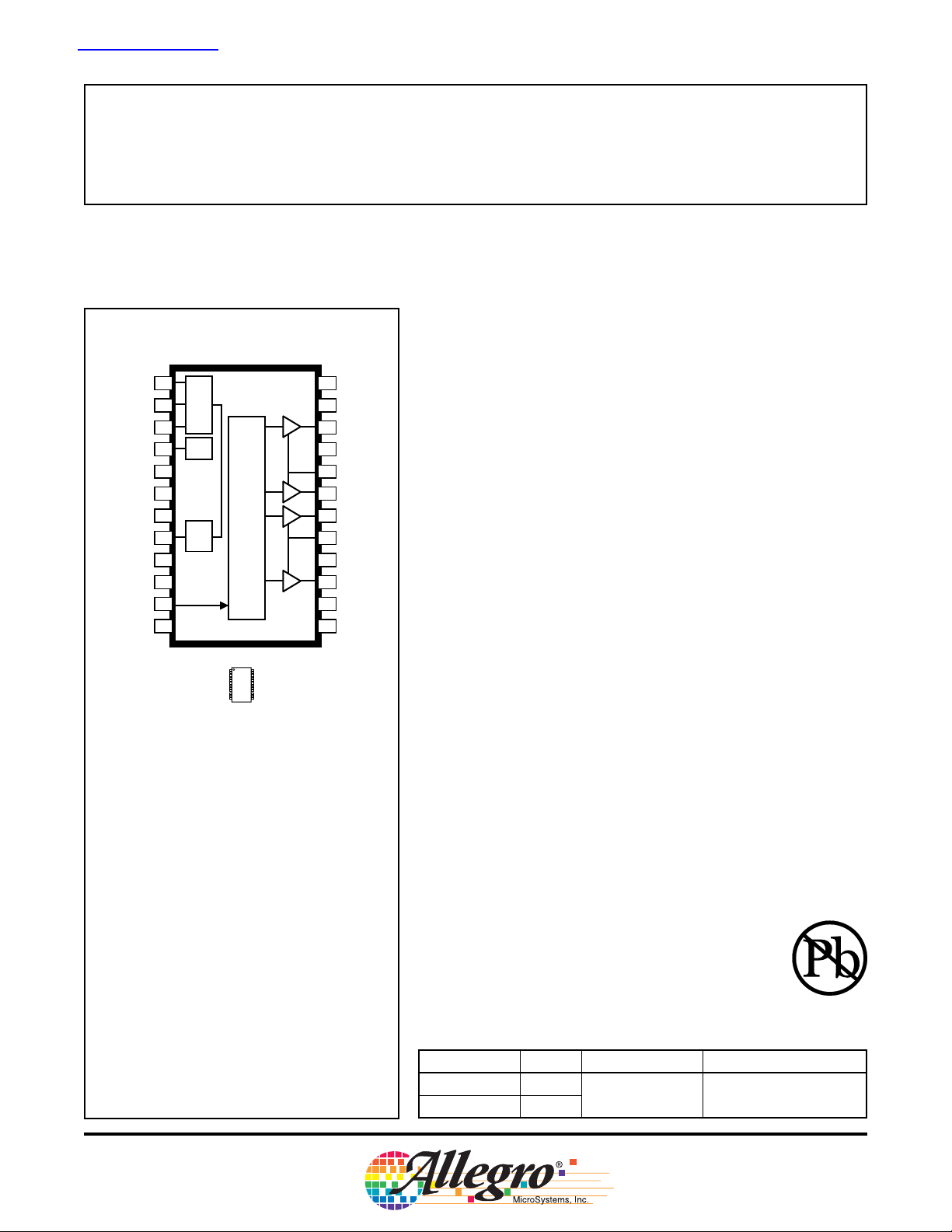
Package LP
CP1
1
CP2
2
Pump
VCP
VREG
MS1
MS2
RESET
ROSC
SLEEP
VDD
STEP
REF
Charge
3
4
Reg
5
6
7
OSC
Translator
& Control Logic
8
9
10
11
12
Approximate Scale 1:1
AB SO LUTE MAX I MUM RAT INGS
Load Supply Voltage,V
Output Current, I
OUT
Logic Input Voltage, V
Sense Voltage, V
SENSE
Reference Voltage, V
Operating Temperature Range
Ambient, T
................................. –20°C to 85°C
A
Junction Temperature, T
Storage Temperature, T
*
Output current rating may be limited by duty cycle,
...................................35 V
BB
......................................... ±2 A
..................... –0.3 V to 7 V
IN
.......................................0.5 V
………..........................4 V
REF
.....................150°C
J(MAX)
.................... –55°C to 150°C
S
ambient temperature, and heat sinking. Under any
set of conditions, do not exceed the specified current
rating or a junction temperature of 150°C.
24
23
22
21
20
19
18
17
16
15
14
13
GND
ENABLE
OUT2B
VBB2
SENSE2
OUT2A
OUT1A
SENSE1
VBB1
OUT1B
DIR
GND
A3983
The A3983 is a complete microstepping motor driver with built-in
translator for easy operation. It is designed to operate bipolar stepper
motors in full-, half-, quarter-, and eighth-step modes, with an output
drive capacity of up to 35 V and ±2 A. The A3983 includes a fixed offtime current regulator which has the ability to operate in Slow or Mixed
decay modes.
The translator is the key to the easy implementation of the A3983.
Simply inputting one pulse on the STEP input drives the motor one
microstep. There are no phase sequence tables, high frequency control
lines, or complex interfaces to program. The A3983 interface is an ideal
fit for applications where a complex microprocessor is unavailable or is
overburdened.
The chopping control in the A3983 automatically selects the current
decay mode (Slow or Mixed). When a signal occurs at the STEP input
pin, the A3983 determines if that step results in a higher or lower
current in each of the motor phases. If the change is to a higher current,
then the decay mode is set to Slow decay. If the change is to a lower
current, then the current decay is set to Mixed (set initially to a fast
decay for a period amounting to 31.25% of the fixed off-time, then
to a slow decay for the remainder of the off-time). This current decay
control scheme results in reduced audible motor noise, increased step
accuracy, and reduced power dissipation.
Internal synchronous rectification control circuitry is provided to
improve power dissipation during PWM operation.
Internal circuit protection includes: thermal shutdown with hysteresis,
undervoltage lockout (UVLO), and crossover-current protection.
Special power-on sequencing is not required.
The A3983 is supplied in a low-profile (1.2 mm maximum), 24-pin
*
TSSOP with exposed thermal pad (package LP). It is also available
in a lead (Pb) free version (suffix –T), with 100% matte tin plated
leadframes.
FEATURES
Low R
Automatic current decay mode detection/selection
Mixed and Slow current decay modes
Synchronous rectification for low power dissipation
Internal UVLO and thermal shutdown circuitry
Crossover-current protection
Use the following complete part number when ordering:
Part Number Pb-free Package Description
A3983SLP –
A3983SLP-T Yes
DS(ON)
outputs
24-pin, TSSOP Exposed thermal pad
26184.29A
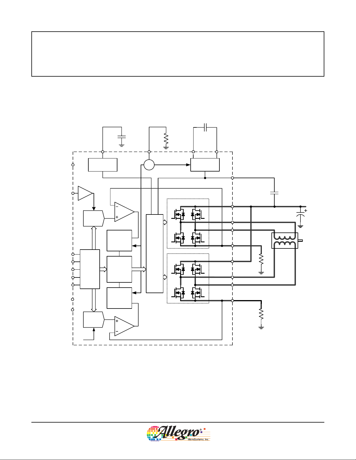
DMOS Microstepping Driver with Translator
Functional Block Diagram
0.22 μF
A3983
0.1 μF
VDD
REF
STEP
DIR
RESET
MS1
MS2
ENABLE
SLEEP
DAC
Translator
VREG
Current
Regulator
PWM Latch
Blanking
Mixed Decay
Control
Logic
PWM Latch
Blanking
Mixed Decay
OSC
ROSC
Gate
Drive
DMOS Full Bridge
DMOS Full Bridge
CP1
Charge
Pump
CP2
VCP
VBB1
OUT1A
OUT1B
SENSE1
VBB2
OUT2A
OUT2B
SENSE2
0.1 μF
R
S1
R
S2
26184.29A
DAC
V
REF
Allegro MicroSystems, Inc.
115 Northeast Cutoff, Box 15036
Worcester, Massachusetts 01615-0036 (508) 853-5000
www.allegromicro.com
2
A3983
DMOS Microstepping Driver with Translator
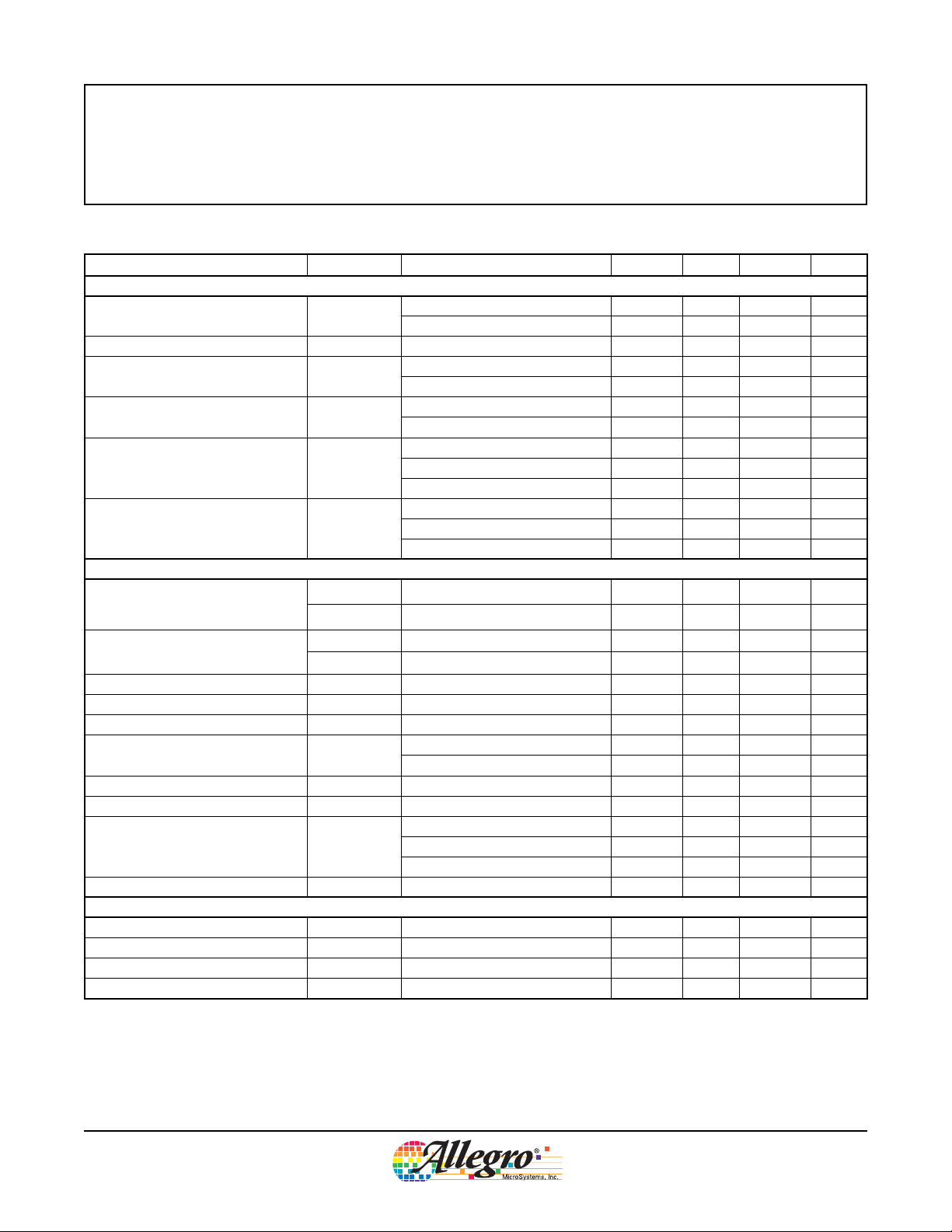
ELECTRICAL CHARACTERISTICS1 at T
Characteristics Symbol Test Conditions Min.
= 25°C, V
A
= 35 V (unless otherwise noted)
BB
Typ.
2
Max. Units
Output Drivers
Load Supply Voltage Range V
Logic Supply Voltage Range V
Output On Resistance R
Body Diode Forward Voltage V
Motor Supply Current I
BB
DD
DSON
F
BB
Operating 8 – 35 V
During Sleep Mode 0 – 35 V
Operating 3.0 – 5.5 V
Source Driver, I
Sink Driver, I
= –1.5 A – 0.350 0.450 Ω
OUT
= 1.5 A – 0.300 0.370 Ω
OUT
Source Diode, IF = –1.5 A – – 1.2 V
Sink Diode, I
f
< 50 kHz – – 4 mA
PWM
= 1.5 A – – 1.2 V
F
Operating, outputs disabled – – 2 mA
Sleep Mode – – 10 μA
f
< 50 kHz – – 8 mA
PWM
Logic Supply Current I
DD
Outputs off – – 5 mA
Sleep Mode – – 10 μA
Control Logic
Logic Input Voltage
Logic Input Current
V
V
I
I
IN(1)
IN(0)
IN(1)
IN(0)
VIN = V
V
= V
IN
DD
DD
×0.7
×0.3
V
×0.7
DD
––
–20 <1.0 20 μA
–20 <1.0 20 μA
––V
V
×0.3
DD
Microstep Select 2 MS2 – 100 – kΩ
Input Hysteresis V
Blank Time
t
Fixed Off-Time
Reference Input Voltage Range V
Reference Input Current I
Current Trip-Level Error
3
Crossover Dead Time t
HYS(IN)
BLANK
t
OFF
REF
REF
err
I
DT
OSC > 3 V 20 30 40 μs
R
= 25 kΩ 23 30 37 μs
OSC
V
REF
V
REF
V
REF
= 2 V, %I
= 2 V, %I
= 2 V, %I
= 38.27% – – ±15 %
TripMAX
= 70.71% – – ±5 %
TripMAX
= 100.00% – – ±5 %
TripMAX
150 300 500 mV
0.7 1 1.3 μs
0–4V
–3 0 3 μA
100 475 800 ns
Protection
Thermal Shutdown Temperature T
Thermal Shutdown Hysteresis T
UVLO Enable Threshold UV
UVLO Hysteresis UV
J
JHYS
LO
HYS
VDD rising 2.35 2.7 3 V
– 165 – °C
–15–°C
0.05 0.10 – V
V
1
Negative current is defined as coming out of (sourcing from) the specified device pin.
2
Typical data are for initial design estimations only, and assume optimum manufacturing and application conditions. Performance may vary for
individual units, within the specified maximum and minimum limits.
3
errI = (I
Trip – IProg
26184.29A
) ⁄ I
Prog
, where I
Prog
= %I
TripMAX
×
I
TripMAX
.
Allegro MicroSystems, Inc.
115 Northeast Cutoff, Box 15036
Worcester, Massachusetts 01615-0036 (508) 853-5000
www.allegromicro.com
3
A3983
DMOS Microstepping Driver with Translator
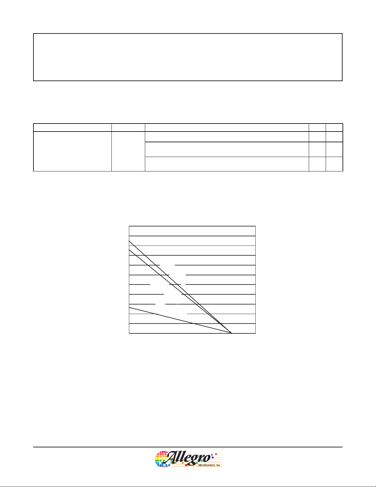
THERMAL CHARACTERISTICS may require derating at maximum conditions, see application information
Characteristic Symbol Test Conditions* Value Units
One-layer PCB, one-sided with copper limited to solder pads 100 ºC/W
One layer PCB, two-sided with copper limited to solder pads and
Package Thermal Resistance
R
θJA
2
3.8 in.
of copper area on each side, connected to GND pins
High-K PCB (multilayer with significant copper areas, based on
JEDEC standard)
*In still air. Additional thermal information available on Allegro Web site.
32 ºC/W
28 ºC/W
Maximum Power Dissipation, P
5.5
5.0
4.5
(W)
D
Power Diss ipation, P
4.0
3.5
3.0
2.5
2.0
1.5
1.0
0.5
0.0
High-K PCB
(R
θJA
= 28
Low-K PCB
(R
θJA
= 32 ºC/W)
Minimum-K PCB
(R
θ
JA
= 100 ºC/W)
ºC/W)
20 40 60 80 100 120 140 160 180
Temperature (°C)
D(max)
26184.29A
Allegro MicroSystems, Inc.
115 Northeast Cutoff, Box 15036
Worcester, Massachusetts 01615-0036 (508) 853-5000
www.allegromicro.com
4

A3983
DMOS Microstepping Driver with Translator
STEP
t
C
MS1, MS2,
RESET, or DIR
Time Duration Symbol Typ. Unit
STEP minimum, HIGH pulse width t
STEP minimum, LOW pulse width t
Setup time, input change to STEP t
Hold time, input change to STEP t
Figure 1. Logic Interface Timing Diagram
t
A
t
D
A
B
C
D
1 μs
1 μs
200 ns
200 ns
t
B
26184.29A
Table 1. Microstep Resolution Truth Table
MS1 MS2 Microstep Resolution Excitation Mode
L L Full Step 2 Phase
H L Half Step 1-2 Phase
L H Quarter Step W1-2 Phase
H H Eighth Step 2W1-2 Phase
Allegro MicroSystems, Inc.
115 Northeast Cutoff, Box 15036
Worcester, Massachusetts 01615-0036 (508) 853-5000
www.allegromicro.com
5

A3983
DMOS Microstepping Driver with Translator
Functional Description
Functional Description
Device Operation. The A3983 is a complete microstep-
ping motor driver with a built-in translator for easy operation
with minimal control lines. It is designed to operate bipolar
stepper motors in full-, half-, quarter-, and sixteenth-step
modes. The currents in each of the two output full-bridges
and all of the N-channel DMOS FETs are regulated with
fixed off-time PMW (pulse width modulated) control circuitry. At each step, the current for each full-bridge is set by
the value of its external current-sense resistor (R
reference voltage (V
), and the output voltage of its DAC
REF
or RS2), a
S1
(which in turn is controlled by the output of the translator).
At power-on or reset, the translator sets the DACs and the
phase current polarity to the initial Home state (shown in figures 2 through 5), and the current regulator to Mixed Decay
Mode for both phases. When a step command signal occurs
on the STEP input, the translator automatically sequences the
DACs to the next level and current polarity. (See table 2 for
the current-level sequence.) The microstep resolution is set
by the combined effect of inputs MS1 and MS2, as shown in
table 1.
When stepping, if the new output levels of the DACs are
lower than their previous output levels, then the decay mode
for the active full-bridge is set to Mixed. If the new output
levels of the DACs are higher than or equal to their previous
levels, then the decay mode for the active full-bridge is set
to Slow. This automatic current decay selection improves
microstepping performance by reducing the distortion of
the current waveform that results from the back EMF of the
motor.
RESET Input (RESET). The RESET input sets the
translator to a predefined Home state (shown in figures 2
through 5), and turns off all of the DMOS outputs. All STEP
inputs are ignored until the RESET input is set to high.
Step Input (STEP). A low-to-high transition on the STEP
input sequences the translator and advances the motor one
increment. The translator controls the input to the DACs and
the direction of current flow in each winding. The size of
the increment is determined by the combined state of inputs
MS1 and MS2.
Microstep Select (MS1 and MS2). Selects the micro-
stepping format, as shown in table 1. MS2 has a 100 kΩ pulldown resistance. Any changes made to these inputs do not take
effect until the next STEP rising edge.
Direction Input (DIR). This determines the direction of
rotation of the motor. When low, the direction will be clockwise and when high, counterclockwise. Changes to this input
do not take effect until the next STEP rising edge.
Internal PWM Current Control. Each full-bridge is
controlled by a fixed off-time PWM current control circuit
that limits the load current to a desired value, I
TRIP
. Initially, a diagonal pair of source and sink DMOS outputs are
enabled and current flows through the motor winding and
the current sense resistor, RSx. When the voltage across R
Sx
equals the DAC output voltage, the current sense comparator resets the PWM latch. The latch then turns off either the
source DMOS FETs (when in Slow Decay Mode) or the sink
and source DMOS FETs (when in Mixed Decay Mode).
The maximum value of current limiting is set by the selection of RSx and the voltage at the VREF pin. The transconductance function is approximated by the maximum value of
current limiting, I
where R
is the resistance of the sense resistor (Ω) and V
S
TripMAX
I
(A), which is set by
TripMAX
= V
REF
/ ( 8 × RS)
REF
is the input voltage on the REF pin (V).
The DAC output reduces the V
output to the current
REF
sense comparator in precise steps, such that
= (%I
I
trip
(See table 2 for %I
TripMAX
TripMAX
/ 100)
×
at each step.)
I
TripMAX
It is critical that the maximum rating (0.5 V) on the SENSE1
and SENSE2 pins is not exceeded.
Fixed Off-Time. The internal PWM current control cir-
cuitry uses a one-shot circuit to control the duration of time
that the DMOS FETs remain off. The one shot off-time, t
is determined by the selection of an external resistor connected from the ROSC timing pin to ground. If the ROSC
OFF
,
26184.29A
Allegro MicroSystems, Inc.
115 Northeast Cutoff, Box 15036
Worcester, Massachusetts 01615-0036 (508) 853-5000
www.allegromicro.com
6

A3983
DMOS Microstepping Driver with Translator
pin is tied to an external voltage > 3 V, then t
defaults to
OFF
30 μs. The ROSC pin can be safely connected to the VDD
pin for this purpose. The value of t
t
≈ R
OFF
OSC
(μs) is approximately
OFF
⁄ 825
Blanking. This function blanks the output of the current
sense comparators when the outputs are switched by the
internal current control circuitry. The comparator outputs are
blanked to prevent false overcurrent detection due to reverse
recovery currents of the clamp diodes, and switching transients related to the capacitance of the load. The blank time,
(μs), is approximately
t
BLANK
t
≈ 1 μs
BLANK
Charge Pump (CP1 and CP2). The charge pump is
used to generate a gate supply greater than that of VBB
for driving the source-side DMOS gates. A 0.1 μF ceramic
capacitor, should be connected between CP1 and CP2. In
addition, a 0.1 μF ceramic capacitor is required between
VCP and VBB, to act as a reservoir for operating the
high-side DMOS gates.
VREG (VREG). This internally-generated voltage is used
to operate the sink-side DMOS outputs. The VREG pin must
be decoupled with a 0.22 μF ceramic capacitor to ground.
VREG is internally monitored. In the case of a fault condition, the DMOS outputs of the A3983 are disabled.
Enable Input (ENABLE). This input turns on or off all of
the DMOS outputs. When set to a logic high, the outputs are
disabled. When set to a logic low, the internal control enables
the outputs as required. The translator inputs STEP, DIR,
MS1, and MS2, as well as the internal sequencing logic, all
remain active, independent of the ENABLE input state.
Shutdown. In the event of a fault, overtemperature
(excess TJ) or an undervoltage (on VCP), the DMOS outputs of the A3983 are disabled until the fault condition is
removed. At power-on, the UVLO (undervoltage lockout)
circuit disables the DMOS outputs and resets the translator to
the Home state.
Sleep Mode (SLEEP). To minimize power consumption
when the motor is not in use, this input disables much of the
internal circuitry including the output DMOS FETs, current
regulator, and charge pump. A logic low on the SLEEP pin
puts the A3983 into Sleep mode. A logic high allows normal
operation, as well as start-up (at which time the A3983 drives
the motor to the Home microstep position). When emerging
from Sleep mode, in order to allow the charge pump to stabilize, provide a delay of 1 ms before issuing a Step command.
Mixed Decay Operation. The bridge can operate in
Mixed Decay mode, depending on the step sequence, as
shown in figures 3 thru 5. As the trip point is reached, the
A3983 initially goes into a fast decay mode for 31.25% of
the off-time. t
for the remainder of t
. After that, it switches to Slow Decay mode
OFF
OFF
.
Synchronous Rectification. When a PWM-off cycle
is triggered by an internal fixed–off-time cycle, load current
recirculates according to the decay mode selected by the
control logic. This synchronous rectification feature turns on
the appropriate FETs during current decay, and effectively
shorts out the body diodes with the low DMOS R
reduces power dissipation significantly, and can eliminate
the need for external Schottky diodes in many applications.
Turning off synchronous rectification prevents the reversal of
the load current when a zero-current level is detected.
DSON
. This
26184.29A
Allegro MicroSystems, Inc.
115 Northeast Cutoff, Box 15036
Worcester, Massachusetts 01615-0036 (508) 853-5000
www.allegromicro.com
7

STEP
Home Microstep Position
Home Microstep Position
100.00
70.71
–70.71
0.00
–100.00
100.00
70.71
–70.71
0.00
–100.00
Phase 2
I
OUT2B
Direction = H
(%)
Phase 1
I
OUT1A
Direction = H
(%)
STEP
Slow
Mixed
Slow
Mixed
Slow
Mixed
Mixed
Slow
Mixed
Slow
Mixed
Slow
Slow
A3983
DMOS Microstepping Driver with Translator
100.00
70.71
Phase 1
I
OUT1A
0.00
Slow
Direction = H
(%)
–70.71
–100.00
100.00
70.71
Home Microstep Position
Phase 2
I
OUT2A
(%)
0.00
Slow
–70.71
–100.00
Direction = H
STEP
100.00
92.39
70.71
(%)
(%)
38.27
0.00
–38.27
–70.71
–92.39
–100.00
100.00
92.39
70.71
38.27
0.00
–38.27
–70.71
–92.39
–100.00
Slow
Slow
Phase 1
I
OUT1A
Direction = H
Phase 2
I
Figure 4. Decay Modes for Quarter-Step Increments
Direction = H
OUT2B
26184.29A
Home Microstep Position
Mixed
Slow
Home Microstep Position
Figure 3. Decay Modes for Half-Step IncrementsFigure 2. Decay Mode for Full-Step Increments
Slow
Mixed
Mixed
Slow
Slow
MixedMixed
Allegro MicroSystems, Inc.
115 Northeast Cutoff, Box 15036
Worcester, Massachusetts 01615-0036 (508) 853-5000
www.allegromicro.com
8

STEP
Phase 1
I
OUT1A
Direction = H
(%)
Phase 2
I
OUT2B
Direction = H
(%)
100.00
92.39
83.15
70.71
55.56
38.27
19.51
0.00
–19.51
–38.27
–55.56
–70.71
–83.15
–92.39
–100.00
100.00
92.39
83.15
70.71
55.56
38.27
19.51
0.00
–19.51
–38.27
–55.56
–70.71
–83.15
–92.39
–100.00
DMOS Microstepping Driver with Translator
Slow
Mixed Slow Mixed Slow
Mixed
Home Microstep Position
Slow
Mixed
A3983
Figure 5. Decay Modes for Eighth-Step Increments
26184.29A
Allegro MicroSystems, Inc.
115 Northeast Cutoff, Box 15036
Worcester, Massachusetts 01615-0036 (508) 853-5000
www.allegromicro.com
9

DMOS Microstepping Driver with Translator
Table 2. Step Sequencing Settings
Home microstep position at Step Angle 45º; DIR = H
A3983
Full
Half
Step
Step
#
123570.71 70.71 45.0
2 4 7 13 –70.71 70.71 135.0
3 6 11 21 –70.71 –70.71 225.0
4 8 15 29 70.71 –70.71 315.0
1/4
Step
#
#
1 1 1 100.00 0.00 0.0
2 3 92.39 38.27 22.5
4 7 38.27 92.39 67.5
3 5 9 0.00 100.00 90.0
6 11 –38.27 92.39 112.5
8 15 –92.39 38.27 157.5
5 9 17 –100.00 0.00 180.0
10 19 –92.39 –38.27 202.5
12 23 –38.27 –92.39 247.5
7 13 25 0.00 –100.00 270.0
14 27 38.27 –92.39 292.5
16 31 92.39 –38.27 337.5
Phase 1
1/8
Current
Step
[% I
#
2 98.08 19.51 11.3
4 83.15 55.56 33.8
6 55.56 83.15 56.3
8 19.51 98.08 78.8
10 –19.51 98.08 101.3
12 –55.56 83.15 123.8
14 –83.15 55.56 146.3
16 –98.08 19.51 168.8
18 –98.08 –19.51 191.3
20 –83.15 –55.56 213.8
22 –55.56 –83.15 236.3
24 –19.51 –98.08 258.8
26 19.51 –98.08 281.3
28 55.56 –83.15 303.8
30 83.15 –55.56 326.3
32 98.08 –19.51 348.8
tripMax
(%)
Phase 2
Current
]
[% I
tripMax
(%)
]
Angle
Step
(º)
26184.29A
Allegro MicroSystems, Inc.
115 Northeast Cutoff, Box 15036
Worcester, Massachusetts 01615-0036 (508) 853-5000
www.allegromicro.com
10

DMOS Microstepping Driver with Translator
Pin List Table
Name Description Number
CP1 Charge pump capacitor 1 1
CP2 Charge pump capacitor 2 2
VCP Reservoir capacitor 3
VREG Regulator decoupling 4
MS1 Logic input 5
MS2 Logic input 6
RESET Logic input 7
ROSC Timing set 8
SLEEP Logic input 9
VDD Logic supply 10
STEP Logic input 11
REF
GND Ground* 13
DIR Logic input 14
OUT1B DMOS Full Bridge 1 Output B 15
VBB1 Load supply 16
SENSE1 Sense resistor for Bridge 1 17
OUT1A DMOS Full Bridge 1 Output A 18
OUT2A DMOS Full Bridge 2 Output A 19
SENSE2 Sense resistor for Bridge 2 20
VBB2 Load supply 21
OUT2B DMOS Full Bridge 2 Output B 22
ENABLE Logic input 23
GND Ground* 24
*The two GND pins must be tied together externally by connecting
to the exposed pad ground plane under the device.
Current trip reference voltage input 12
A3983
26184.29A
Allegro MicroSystems, Inc.
115 Northeast Cutoff, Box 15036
Worcester, Massachusetts 01615-0036 (508) 853-5000
www.allegromicro.com
11

DMOS Microstepping Driver with Translator
LP Package, 24-Pin TSSOP with Exposed Thermal Pad
A3983
26184.29A
Allegro MicroSystems, Inc.
115 Northeast Cutoff, Box 15036
Worcester, Massachusetts 01615-0036 (508) 853-5000
www.allegromicro.com
12

A3983
DMOS Microstepping Driver with Translator
26184.29A
The products described here are manufactured under one or
more U.S. patents or U.S. patents pending.
Allegro MicroSystems, Inc. reserves the right to make, from time
to time, such de par tures from the detail spec i fi ca tions as may be
required to permit improvements in the per for mance, reliability,
or manufacturability of its products. Before placing an order, the
user is cautioned to verify that the information being relied upon is
current.
Allegro products are not authorized for use as critical components in life-support devices or sys tems without express written
approval.
The in for ma tion in clud ed herein is believed to be ac cu rate and
reliable. How ev er, Allegro MicroSystems, Inc. assumes no re spon si bil i ty for its use; nor for any in fringe ment of patents or other
rights of third parties which may result from its use.
Copyright©2005 AllegroMicr osystems, Inc.
Allegro MicroSystems, Inc.
115 Northeast Cutoff, Box 15036
Worcester, Massachusetts 01615-0036 (508) 853-5000
www.allegromicro.com
13
 Loading...