

& Control Logic
R
R
A
A
查询A3980供应商查询A3980供应商
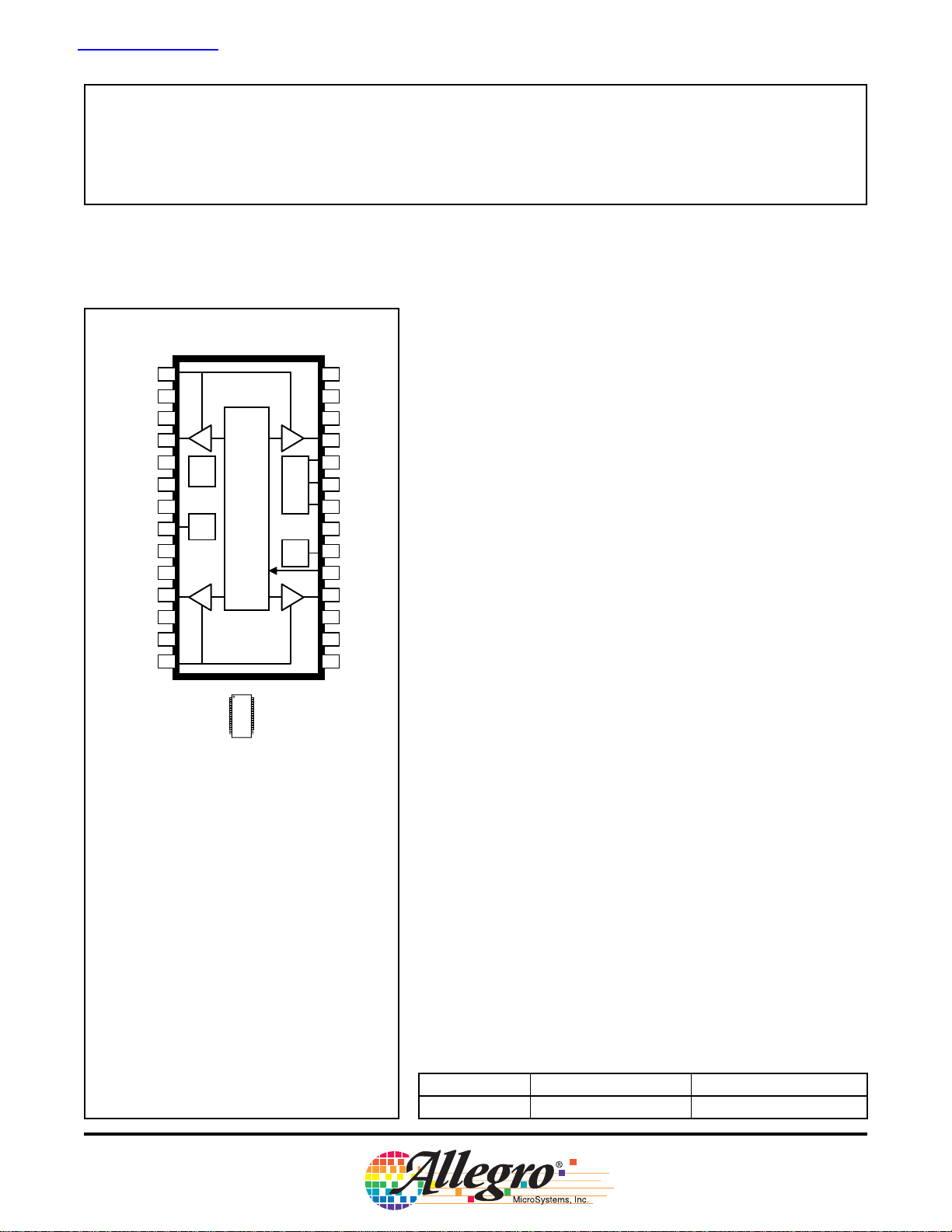
Automotive DMOS Microstepping Driver with Translator
SENSE1
SENSE2
OUT1
PFD
RC1
AGND
REF
RC2
VDD
OUT2
MS2
MS1
1
S
2
DI
3
4
5
PWM
6
7
÷
8
8
9
VDD
10
11
12
13
14
Package LP
Timer
Translator
Reg
VBB1
Charge
VBB2
Data Sheet
26184.26A
A3980
The A3980 is a complete microstepping motor driver with built-in
translator for easy operation. It is designed to operate bipolar stepper
motors in full-, half-, eighth-, and sixteenth-step modes, at up to 35 V
VBB1
28
SLEEP
27
ENABLE
26
OUT1B
25
CP2
24
CP1
23
Pump
VCP
22
PGND
21
VREG
20
STEP
19
OUT2B
18
FF2
17
FF1
16
VBB2
15
and ±1 A. The A3980 includes a fi xed off-time current regulator which
has the ability to operate in slow, fast, or mixed decay modes. This
results in reduced audible motor noise, increased step accuracy, and
reduced power dissipation.
The translator is the key to the easy implementation of the A3980.
Simply inputting one pulse on the step input drives the motor one
microstep. There are no phase sequence tables, high frequency control
lines, or complex interfaces to program. The A3980 interface is an ideal
fi t for applications where a complex µP is unavailable or overburdened.
Internal synchronous rectifi cation control circuitry is provided to
improve power dissipation during PWM operation.
Internal circuit protection includes: thermal shutdown with hysteresis,
overvoltage lockout (OVLO), undervoltage lockout (UVLO), and
crossover current protection. Special power-up sequencing is not
required. In addition, two diagnostic fault fl ags provide indication of
shorts or opens on the motor windings.
Approximate Scale 1:1
AB SO LUTE MAX I MUM RAT INGS
Load Supply Voltage, 500 ms,VBB.....................50 V
Logic Supply Voltage, V
Logic Input Voltage
V
(t
Sense Voltage, V
................................. –0.3 V to VDD + 0.3 V
IN
< 30 ns) ....................... –1.0 V to VDD + 1 V
W
SENSE
Reference Voltage, V
Package Power Dissipation (TA = +25ºC), P
"High-K" PCB1..............................R
Typical PCB
2
..................................R
Operating Temperature Range
Junction Temperature, T
Storage Temperature, TS..........–55°C to +150°C
1
Measured on a JEDEC-standard "High-K" 4-layer PCB.
2
Measured on a typical two-sided PCB with 3 in.2 copper
ground area.
................................7.0 V
DD
.......................................0.5 V
………............. 0 V to V
REF
D
28ºC/W
θJA
38ºC/W
θJA
...........–40°C to +150°C
J
DD
The A3980 is supplied in a low-profi le (1.1 mm) 28L TSSOP with
exposed thermal pad (part number suffi x LP).
FEATURES
Typical application up to ±1 A, 35 V output rating
Low R
outputs, 0.67 Ω source, 0.54 Ω sink typical
DS(ON)
Automatic current decay mode detection/selection
3.0 V to 5.5 V logic supply voltage range
Mixed, fast, and slow current decay modes
Synchronous rectifi cation for low power dissipation
Internal OVLO, UVLO, and thermal shutdown circuitry
Crossover current protection
Short to supply/ground and short/open load diagnostics
APPLICATIONS
Automotive stepper motors
Engine management
Headlamp positioning
Use the following complete part number when ordering:
Part Number Package Description
A3980KLP 28-pin, TSSOP Exposed thermal pad
5 V
RT1C
RT2C
VDD
STEP
DIR
MS1
MS2
RC1
T1
SR
SLEEP
ENABLE
PFD
RC2
T2
Automotive DMOS Microstepping Driver with Translator
Functional Block Diagram
C
CP
VREG
DAC
Translator
DAC
V
REF
SENSE 1
PWM Latch
Blanking
Mixed Decay
Control
Logic
PWM Latch
Blanking
Mixed Decay
SENSE 2
V
REF
Gate
Drive
DMOS Full Bridge
DMOS Full Bridge
OVLO
UVLO
OVERTEMP
SHORT SENSE
OPEN SENSE
CP2
Charge
Pump
Voltage
Regulator
VDD
VCP
VBB
OUT1A/1B
OUT2A/2B
SENSE1
SENSE2
CP1
VCP
VBB1
OUT1A
OUT1B
SENSE1
VBB2
OUT2A
OUT2B
SENSE2
RS2C
C
CS
R
C
S1
S1
S2
A3980
VBATT
Data Sheet
26184.26A
AGND
REF
FF1 FF2
PGND
www.allegromicro.com
115 Northeast Cutoff, Box 15036
Worcester, Massachusetts 01615-0036 (508) 853-5000
2

A3980
Automotive DMOS Microstepping Driver with Translator
Data Sheet
26184.26A
ELECTRICAL CHARACTERISTICS at T
Characteristics Symbol Test Conditions Min. Typ.1Max. Units
Output Drivers
Load Supply Voltage Range V
Output Leakage Current
Output-On Resistance R
Body Diode Forward Voltage V
Motor Supply Current I
Logic Supply Current I
2
I
DSON
Logic Interface
Logic Supply Voltage Range V
Input Low Voltage V
Input High Voltage V
Input Hysteresis V
Input Current
Output Low Voltage V
Output High Voltage V
STEP Pin Low t
STEP Pin High t
Setup Time for Input Change to STEP t
Hold Time for Input Change from STEP t
Wake-Up Time from SLEEP t
2
STPL
STPH
Continued on next page
= –40°C to +150ºC, V
J
Driving
Operating
BB
Sleep mode
V
= V
OUT
DSS
BB
DD
DD
IH
IHYS
I
IN
OL
OH
V
Source driver, I
Sink driver, I
Source driver, I
Sink driver, I
Source diode, IF = –1 A
F
Sink diode, IF = 1 A
f
PWM
Operating, outputs disabled
Sleep mode
f
PWM
Outputs off
Sleep mode
Operating 3.0 5.0 5.5 V
–––
IL
–
–
–
IO = 3 mA
IO = –200 µA 2.8
= 0 V
OUT
< 50 kHz
< 50 kHz
BB
–
–
MS1, MS2, DIR 200
SU
MS1, MS2, DIR 200
H
–––
EN
= 14 V, VDD = 3.0 to 5.5 V (unless otherwise noted)
BB
= –1 A, TA < 25ºC
OUT
= 1 A, TA < 25ºC
OUT
= –1 A, TA < 125ºC
OUT
= 1 A, TA < 125ºC
OUT
8
7
0
–
–
–
–
< 1.0
< 1.0
0.51
0.45
0.87
0.72
––
––
––
0.7 V
DD
200 300 500 mV
–20 < ±1 20 µA
––
––
V
OVB
50
35
20
–20
0.86
0.65
1.06
0.83
1.4
1.4
8
6
20
12
10
20
0.3 V
DD
0.4 V
––
1
1
––
––
––
––
1ms
V
µA
Ω
Ω
V
mA
mA
µA
mA
mA
µA
V
V
V
µs
µs
ns
ns
www.allegromicro.com
115 Northeast Cutoff, Box 15036
Worcester, Massachusetts 01615-0036 (508) 853-5000
3

A3980
Automotive DMOS Microstepping Driver with Translator
Data Sheet
26184.26A
ELECTRICAL CHARACTERISTICS (continued) at T
Characteristics Symbol Test Conditions Min.
= –40°C to +150ºC, V
J
= 14 V, VDD = 3.0 to 5.5 V (unless otherwise noted)
BB
1
Typ.
Max. Units
Current Control
Blank Time t
Fixed Off Time T
Mixed Decay Trip Points
Crossover Dead Time t
Recommended Reference Input Voltage V
) ⁄ I
Prog
2
3
, where I
Prog
= %I
Reference Input Current
Current Trip-Level Error
Thermal Protection
Thermal Shutdown T
Thermal Shutdown Hysteresis T
Diagnostics
Max V
Max VDS on Low-Side Bridge FETs V
VDS Fault Measurement Delay t
Minimum Load Current I
V
V
V
VDD Enable Threshold V
V
1
for individual units, within the specifi ed maximum and minimum limits.
2
3
on High-Side Bridge FETs V
DS
Overvoltage Lockout V
BB
Overvoltage Lockout Hysteresis V
BB
Undervoltage Lockout V
REG
Enable Threshold Hysteresis V
DD
Typical data are for initial design estimations only, and assume optimum manufacturing and application conditions. Performance may vary
Negative current is defi ned as coming out of (sourcing from) the specifi ed device pin.
errI = (I
Trip – IProg
BLANK
PFD
PFD
I
REF
err
DSHT
DSLT
SCT
OVBH
UVDH
TripMAX×
RT = 56 K , CT = 680 pF 700 950 1200 ns
RT = 56 K , CT = 680 pF 30 38 46 µs
OFF
H
––
L
DT
REF
–
–
100 475 800 ns
–
V
= 4 V, %I
REF
V
I
SD
SDH
= 4 V, %I
REF
V
= 4 V, %I
REF
–
––
Sampled after t
Sampled after t
TripMAX
TripMAX
TripMAX
BLANK
BLANK
= 38%
= 70%
= 100%
+ t
SCT
+ t
SCT
160 170 180 ºC
––
w.r.t. I
OC
VBB rising 32 34 36 V
OVB
at Home position
TRIPMAX
–
V
UVR
UVD
falling 5.3 5.7 6.0 V
REG
VDD rising 2.45 2.7 2.95 V
–
I
.
TripMAX
0.60 V
DD
0.21 V
DD
0.8
–3 0 3 µA
–
––
15
–
–
–
2
50 100
1.5
1.5
700
35
–
–
4V
±15
±10
±5
–
–
–
–
–
4V
–
V
%
ºC
V
V
ns
%
mV
www.allegromicro.com
115 Northeast Cutoff, Box 15036
Worcester, Massachusetts 01615-0036 (508) 853-5000
4
Automotive DMOS Microstepping Driver with Translator
Logic Interface Timing Diagram
A3980
Data Sheet
26184.26A
STEP
t
SU
MS1, MS2,
or DIR
t
EN
SLEEP
Table 1. Microstep Resolution Truth Table
MS1 MS2 Microstep Resolution
L L Full Step
H L Half Step
L H Eighth Step
H H Sixteenth Step
t
STPH
t
H
t
STPL
Table 2. Fault Report by Fault Flags
FF1 FF2 Fault
LL
H L Short to Ground
L H Short to Supply
H H None
UVLO, OVLO, Overtemperature,
Open Load, or Shorted Load
www.allegromicro.com
115 Northeast Cutoff, Box 15036
Worcester, Massachusetts 01615-0036 (508) 853-5000
5

Automotive DMOS Microstepping Driver with Translator
Table 3. Step Sequencing Settings
Home microstep position at Step Angle 45º; DIR = H
A3980
Data Sheet
26184.26A
Full
Step
#
Half
Step
#
1/8
Step
#
1/16
Step
#
Phase 1
Current
[% I
tripMax
(%)
]
[% I
Phase 2
Current
tripMax
(%)
Step
]
Angle
(º)
Full
Step
#
Half
Step
#
1/8
Step
#
1/16
Step
#
Phase 1
Current
[% I
tripMax
(%)
[% I
]
Phase 2
Current
tripMax
(%)
]
1 1 1 100.00 0.00 0.0 5 17 33 –100.00 0.00 180.0
2 99.52 9.80 5.6 34 –99.52 –9.80 185.6
2 3 98.08 19.51 11.3 18 35 –98.08 –19.51 191.3
4 95.69 29.03 16.9 36 –95.69 –29.03 196.9
3 5 92.39 38.27 22.5 19 37 –92.39 –38.27 202.5
6 88.19 47.14 28.1 38 –88.19 –47.14 208.1
4 7 83.15 55.56 33.8 20 39 –83.15 –55.56 213.8
8 77.30 63.44 39.4 40 –77.30 –63.44 219.4
1 2 5 9 70.71 70.71 45.0 3 6 21 41 –70.71 –70.71 225.0
10 63.44 77.30 50.6 42 –63.44 –77.30 230.6
6 11 55.56 83.15 56.3 22 43 –55.56 –83.15 236.3
12 47.14 88.19 61.9 44 –47.14 –88.19 241.9
7 13 38.27 92.39 67.5 23 45 –38.27 –92.39 247.5
14 29.03 95.69 73.1 46 –29.03 –95.69 253.1
8 15 19.51 98.08 78.8 24 47 –19.51 –98.08 258.8
16 9.80 99.52 84.4 48 –9.80 –99.52 264.4
3 9 17 0.00 100.00 90.0 7 25 49 0.00 –100.00 270.0
18 –9.80 99.52 95.6 50 9.80 –99.52 275.6
10 19 –19.51 98.08 101.3 26 51 19.51 –98.08 281.3
20 –29.03 95.69 106.9 52 29.03 –95.69 286.9
11 21 –38.27 92.39 112.5 27 53 38.27 –92.39 292.5
22 –47.14 88.19 118.1 54 47.14 –88.19 298.1
12 23 –55.56 83.15 123.8 28 55 55.56 –83.15 303.8
24 –63.44 77.30 129.4 56 63.44 –77.30 309.4
2 4 13 25 –70.71 70.71 135.0 4 8 29 57 70.71 –70.71 315.0
26 –77.30 63.44 140.6 58 77.30 –63.44 320.6
14 27 –83.15 55.56 146.3 30 59 83.15 –55.56 326.3
28 –88.19 47.14 151.9 60 88.19 –47.14 331.9
15 29 –92.39 38.27 157.5 31 61 92.39 –38.27 337.5
30 –95.69 29.03 163.1 62 95.69 –29.03 343.1
16 31 –98.08 19.51 168.8 32 63 98.08 –19.51 348.8
32 –99.52 9.80 174.4 64 99.52 –9.80 354.4
Step
Angle
(º)
www.allegromicro.com
115 Northeast Cutoff, Box 15036
Worcester, Massachusetts 01615-0036 (508) 853-5000
6

Phase 1
100.00
70.71
–70.71
–100.00
100.00
70.71
–70.71
–100.00
Phase 2
I
OUT2B
Direction = H
(%)
Phase 1
I
OUT1B
Direction = H
(%)
Home Microstep Position
I
OUT1B
Direction = H
(%)
Phase 2
I
OUT2B
Direction = H
(%)
100.00
70.71
–70.71
–100.00
100.00
70.71
A3980
Automotive DMOS Microstepping Driver with Translator
Home Microstep Position
Data Sheet
26184.26A
Figure 5. Full Step
STEP
Phase 1
I
OUT1B
Direction = H
(%)
Phase 2
I
Direction = H
OUT2B
(%)
–70.71
–100.00
100.00
92.39
83.15
70.71
55.56
38.27
19.51
0.00
–19.51
–38.27
–55.56
–70.71
–83.15
–92.39
–100.00
100.00
92.39
83.15
70.71
55.56
38.27
19.51
0.00
–19.51
–38.27
–55.56
–70.71
–83.15
–92.39
–100.00
Figure 6. Half Step
Slow
Mixed Slow Mixed Slow
Mixed
Home Microstep Position
Slow
Mixed
Figure 7. Eighth Step
www.allegromicro.com
115 Northeast Cutoff, Box 15036
Worcester, Massachusetts 01615-0036 (508) 853-5000
7

STEP
100.00
95.69
88.19
83.15
77.30
70.71
63.44
55.56
47.14
38.27
29.03
19.51
(%)
(%)
9.8
0.00
–9.8
–19.51
–29.03
–38.27
–47.14
–55.56
–63.44
–70.71
–77.30
–83.15
–88.19
–95.69
–100.00
100.00
95.69
88.19
83.15
77.30
70.71
63.44
55.56
47.14
38.27
29.03
19.51
9.8
0.00
–9.8
–19.51
–29.03
–38.27
–47.14
–55.56
–63.44
–70.71
–77.30
–83.15
–88.19
–95.69
–100.00
Slow
Phase 1
I
OUT1B
Direction = H
Phase 2
I
OUT2B
Direction = H
Figure 8. Sixteenth Steps
A3980
Automotive DMOS Microstepping Driver with Translator
MixedSlow MixedSlow
Home Microstep Position
Mixed
MixedSlow Slow
Data Sheet
26184.26A
www.allegromicro.com
115 Northeast Cutoff, Box 15036
Worcester, Massachusetts 01615-0036 (508) 853-5000
8

A3980
Automotive DMOS Microstepping Driver with Translator
Functional Description
Data Sheet
26184.26A
Device Operation. The A3980 is a complete microstep-
ping motor driver with a built-in translator for easy operation
with minimal control lines. It is designed to operate bipolar
stepper motors in full-, half-, eighth-, and sixteenth-step
modes. The currents in each of the two output full-bridges
and all of the N-channel DMOS FETs are regulated with
fi xed off-time PMW (pulse width modulated) control circuitry. At each step, the current for each full-bridge is set by
the value of its external current-sense resistor (R
reference voltage (V
), and the output voltage of its DAC
REF
(which in turn is controlled by the output of the translator).
At power-up, the translator resets to the Home state, in which
the motor is driven to the Home microstep position, where
both phase currents are set to +70%. Then the translator sets
the voltage regulator to mixed decay mode for both phases.
When a step command signal occurs on the STEP input, the
translator automatically sequences the DACs to the next
level and current polarity. (See table 3 for the current-level
sequence.) The microstep resolution is set by the combined
effect of inputs MS1 and MS2, as shown in table 1.
When stepping, if the new output levels of the DACs are
lower than their previous output levels, then the decay mode
(fast, slow, or mixed decay) for the active full-bridge is set
by the PFD input. If the new output levels of the DACs are
higher than or equal to their previous levels, then the decay
mode for the active full-bridge is set to slow decay. This
automatic current decay selection improves microstepping
performance by reducing the distortion of the current waveform that results from the back EMF of the motor.
or RS2), a
S1
increment. The translator controls the input to the DACs and
the direction of current fl ow in each winding. The size of
the increment is determined by the combined state of inputs
MS1 and MS2.
Microstep Select (MS1 and MS2). Selects the micro-
stepping format, as shown in table 1. Any changes made to
these inputs do not take effect until the next STEP rising edge.
Direction Input (DIR). This determines the direction of
rotation of the motor. When low, the direction will be clockwise and when high, counterclockwise. Changes to this input
do not take effect until the next STEP rising edge.
Internal PWM Current Control. Each full-bridge is
controlled by a fi xed off-time PWM current control circuit
that limits the load current to a desired value, I
a diagonal pair of source and sink DMOS FETs are enabled
and current fl ows through the motor winding and the current
sense resistor, RS. When the voltage across RS equals the
DAC output voltage, the current sense comparator resets the
PWM latch. The latch then turns off either the source DMOS
(when in slow decay mode) or the sink and source DMOSs
(when in fast or mixed decay modes).
The transconductance function is approximated by the maximum value of current limiting, I
I
TripMAX
= V
REF
TripMAX
(A), which is set by
⁄ (8 × RS)
where RS is the resistance of the sense resistor (Ω) and V
is the input voltage on the REF pin (V).
. Initially,
TRIP
REF
Home Microstep Position. At power-up, or after
a UVLO (undervoltage lockout) condition caused by low
voltage on VDD, the translator in the A3980 resets the motor
to the Home microstep position. This corresponds to the 45°
position, which is the step where both phase currents are
+70%. Referring to table 3, for full-step mode this is step
1, for half-step this is step 2, for eighth-step this is step 5,
and for sixteenth-step this is step 9. In table 3 and fi gures 5
through 8, the Home microstep position is indicated.
Step Input (STEP). A low-to-high transition on the STEP
input sequences the translator and advances the motor one
www.allegromicro.com
115 Northeast Cutoff, Box 15036
Worcester, Massachusetts 01615-0036 (508) 853-5000
The DAC output reduces the V
output to the current
REF
sense comparator in precise steps, such that
I
= (%I
trip
(See table 3 for %I
TripMAX
TripMAX
⁄ 100)
×
at each step.)
I
TripMAX
It is critical that the maximum rating (0.5 V) on the SENSE
pin is not exceeded. For full-step mode, V
can be applied
REF
up to the maximum rating of VDD, because the peak sense
value is 70% of maximum:
REF
(0.707 ⁄ 8)
×
V
9

A3980
Automotive DMOS Microstepping Driver with Translator
Data Sheet
26184.26A
as shown in table 3. In all other modes, V
should not be
REF
allowed to exceed 4 V, because the peak sense value can
reach V
⁄ 8, or 100%.
REF
Fixed Off-Time. The internal PWM current control
circuitry uses a one-shot circuit to control the duration of
time that the DMOS FETs remain off. The one shot off-time,
t
, is determined for each of the two phases by the combi-
OFF
nation of an external resistor (RT) and a capacitor (CT). One
combination is connected from the timing terminal RC1 to
ground, and the other similarly connected to RC2 . t
OFF
(ns)
is approximated by
t
OFF
= R
C
×
T
T
over a range of values from CT= 470 pF to 1500 pF and from
RT = 12 kΩ to 100 kΩ.
RC Blanking. In addition to the fi xed off-time of the
PWM control circuit, the CT component sets the comparator
blanking time. This function blanks the output of the current
sense comparators when the outputs are switched by the
internal current control circuitry. The comparator outputs are
blanked to prevent false overcurrent detection due to reverse
recovery currents of the clamp diodes, and switching transients related to the capacitance of the load. The blank time,
t
(ns), can be approximated by
BLANK
t
= 1400 × C
BLANK
where CT is the value of the capacitor CT (nF).
The blank time should be as short as possible, without causing a false fault detection, to ensure that power dissipation
during a fault condition is minimized. The blank time also
defi nes the minimum duration of time that the full-bridge
DMOS outputs cause the load current to rise. To ensure
correct detection of motor faults, the minimum on-time is
extended by an additional fault sampling time, t
minimum on-time, t
MINON
t
MINON
is then
= t
BLANK
+ t
T
SCT
SCT
. The
capacitor (C
), capable of withstanding the battery volt-
CP
age VBATT, should be connected between CP1 and CP2.
In addition, a 100 nF ceramic capacitor (CCS)is required
between VCP and VBB, to act as a reservoir for operating
the high-side DMOS devices. The voltage on CCS is limited to
the charge pump voltage, which is always less than 10 V.
VREG (VREG). This internally-generated voltage is used
to operate the sink-side DMOS FETs. The VREG terminal
must be decoupled with a 220 nF (10V) capacitor to ground.
VREG is internally monitored. In the case of a fault condition, the DMOS outputs of the A3980 are disabled.
Enable Input (ENABLE). This input simply turns off all
of the DMOS outputs. When set to a logic high, the outputs
are disabled. When set to a logic low, the internal control
enables the outputs as required. The translator inputs (STEP,
DIR, MS1, and MS2), as well as the internal sequencing
logic, all remain active, independent of the ENABLE input
state.
Sleep Mode (SLEEP). To minimize power consumption
when the motor is not in use, this input disables much of the
internal circuitry including the output DMOS FETs, voltage
regulator, and charge pump. A logic low on the SLEEP terminal puts the A3980 into Sleep mode. A logic high allows
normal operation, as well as start-up (at which time the
A3980 drives the motor to the Home microstep position).
Percent Fast Decay Input (PFD). When a STEP input
signal commands an output current level that is lower than
that of the previous step, it switches the output current decay
to slow, fast, or mixed decay mode, depending on the voltage
level at the PFD input, as shown in the following table.
(0.21
Lower PFD Input
Voltage Level
> (0.6 × V
V
PFD
VDD ) ≤ V
×
< (0.21 × VDD)
V
PFD
≤ (0.6 × V
PFD
DD
)
DD
)
Decay Mode
Slow
Mixed
Fast
Charge Pump (CP1 and CP2). The charge pump is
used to generate a gate supply greater than that of VBB for
driving the source-side DMOS gates. A 100 nF ceramic
www.allegromicro.com
115 Northeast Cutoff, Box 15036
Worcester, Massachusetts 01615-0036 (508) 853-5000
Mixed Decay Operation. Depending on the step
sequence, if the voltage on the PFD pin is between
0.6
V
×
and 0.21
DD
V
, the full-bridge can operate in
×
DD
10

A3980
Automotive DMOS Microstepping Driver with Translator
Data Sheet
26184.26A
mixed decay mode, as shown in fi gures 5 through 8. As the
trip point is reached, the A3980 goes into fast decay mode
until the voltage on the RC pin decays to the same level as the
voltage applied to the PFD pin. The duration of time that the
bridge operates in fast decay mode, tFD (ns), is estimated by
tFD = R
over a range of values from CT= 470 pF to 1500 pF and from
= 12 kΩ to 100 kΩ.
R
T
After this fast decay period, the A3980 switches to slow
decay mode for the remainder of the fi xed off-time period.
C
×
T
ln[0.6 (V
×
T
DD
⁄ V
PFD
)]
Synchronous Rectifi cation. When a PWM-off cycle
is triggered by an internal fi xed-off-time cycle, load current
recirculates according to the decay mode selected by the
control logic. The synchronous rectifi cation feature turns on
the appropriate FETs during current decay, and effectively
shorts out the body diodes with the low DMOS R
reduces power dissipation signifi cantly, and eliminates the
need for external Schottky diodes. Synchronous rectifi cation
has two modes: Active mode and Disabled mode (described
below).
DSON
. This
Active Mode. When the input on the SR terminal is set
at logic low, Active mode is enabled. This mode allows
synchronous rectifi cation to occur, but when a zero current
level is detected, it also prevents reversal of the load current
by turning off synchronous rectifi cation. This prevents the
motor winding from conducting in the reverse direction.
Disabled Mode. When the input on the SR terminal is set
at logic high, Disabled mode takes effect. This mode disables
synchronous rectifi cation. This mode is typically used when
external diodes are required to transfer power dissipation
from the A3980 package to the external diodes.
Shutdown. In the event of an overtemperature fault or
an undervoltage fault on VREG, the DMOS outputs of the
A3980 are disabled until the fault condition is removed. In
the case of an overvoltage fault, the sink DMOS FETs are
switched on, and the source FETs off. At power-up, and in
the event of low VDD, the UVLO circuit disables the DMOS
outputs until VDD reaches the minimum level. Once VDD is
above the minimum level, the translator resets to the Home
state and the DMOS outputs are re-enabled.
Thermal Protection. All drivers are turned off when the
junction temperature reaches the thermal shutdown value,
typically 170°C. This is intended only to protect the A3980
from failures due to excessive junction temperatures. Thermal protection will not protect the A3980 from continuous
short circuits, and additional fault diagnostics are integrated for
this purpose. Thermal shutdown has a hysteresis of approximately 15°C.
Diagnostic Features. The A3980 includes monitor
circuits that can detect shorts to VBB, shorts to ground, and
shorted or open circuit load. Short circuits are detected by
monitoring the voltage across the driving DMOS FETs and
the open load is detected by monitoring the phase current
when the motor is in the Home microstep position. All fault
detection takes place following a delay after the blank time.
Short to VBB. A short from any of the motor connections
to the battery or VBB connection is detected by monitoring
the voltage across the bottom FETs in each full-bridge. When
the FET is on, the voltage should be no greater than the
V
value defi ned in the Electrical Characteristics table.
DSLT
Short to Ground. A short from any of the motor connections to ground is detected by monitoring the voltage across
the top FETs in each full-bridge. When the FET is turned
on, the voltage should be no greater than the V
defi ned in the Electrical Characteristics table.
Shorted Load. A short across the load is detected by
monitoring the voltage across both the top and bottom FETs
in each full-bridge.
Short Fault Operation. Because motor capacitance may
cause the measured voltages to show a fault as the full-bridge
switches, voltages are not sampled until after the blank
time plus an internally-generated delay, t
circuit has been detected, all outputs for the faulty phase are
disabled until the next step command. At the next step command, the outputs are re-enabled and the voltage across the
FET is resampled.
SCT
value
DSHT
. Once a short
www.allegromicro.com
115 Northeast Cutoff, Box 15036
Worcester, Massachusetts 01615-0036 (508) 853-5000
11

A3980
Automotive DMOS Microstepping Driver with Translator
Data Sheet
26184.26A
While the fault persists, the A3980 continues this cycle at
each step command: enabling the outputs for a short period,
and then disabling the outputs. This allows the A3980 to
handle a continuous short circuit without damage. If, while
stepping rapidly, a short circuit appears and no action is
taken, the repeated short-circuit current pulses eventually
cause the temperature of the A3980 to rise and an overtemperature fault occurs.
Open Load Fault Operation. An open load is detected
by monitoring the phase current while the motor is in the
Home microstep position, after a time duration of the blank
time plus an internally-generated delay, t
microstep position, each phase current should be 70% of
I
TripMAX
. If the measured current is less than half of this
expected current level (less than 35% of I
open load condition is reported on the fi rst step command.
Because the A3980 translator is reset to the Home state at
power-up, an existing open load is detected at the initial step
command. If an open load condition appears while stepping, then it is detected after the translator cycles through
the Home state. Although the A3980 continues to drive the
. At the Home
SCT
TripMAX
), then an
DMOS outputs during an open load condition, it does not
clear the fault fl ags until the next Home state occurs.
Supply Monitors. External and internal supplies are
monitored to ensure that they are within the correct operating range. If the main supply exceeds the overvoltage limit,
V
, the fault fl ags are set and the A3980 enters a safety
OVB
mode in which all low-side DMOS FETs are enabled and all
high-side DMOS FETs are disabled. This allows the A3980
to survive a load dump transient condition that has up to
50 V on VBATT and a duration of up to 500 ms. If the internal regulator V
tive undervoltage limits (V
or the logic supply VDD go below their respec-
REG
UVR
or V
), then: the fault fl ags are
UVD
set, the DMOS outputs are disabled, and the internal logic is reset
to the power-on state (the translator is set to the Home state).
Diagnostic Fault Flags (FF1, FF2). Diagnostic fault
conditions are reported using the two fault fl ag outputs.
These are active-low outputs which are coded as shown in
table 2 to discriminate between the fault conditions. When
both fault fl ags are high, no fault exists.
www.allegromicro.com
115 Northeast Cutoff, Box 15036
Worcester, Massachusetts 01615-0036 (508) 853-5000
12

Automotive DMOS Microstepping Driver with Translator
Application Information
The A3980 is a power circuit, therefore careful consideration must be given to power dissipation and the effects
of high currents on interconnect and supply wiring.
Power Dissipation. A fi rst order approximation of
the power dissipation in the A3980 can be determined
by examining the power dissipation in each of the
two full-bridges during each of the operation modes.
When synchronous rectifi cation is used, current fl ow
most of the time through the DMOS FETs that are
switched on. When synchronous rectifi cation is not
used, the current fl ows through the body diode of
the DMOS FETs during the decay phase. The use of
fast or slow decay also affects the dissipation. All the
above combinations can be calculated from fi ve basic
DMOS output states, shown in the following illustrations.
Data Sheet
26184.26A
A3980
+
M
Drive Current Ramp
Diagonally opposite DMOS
output transistors are on. Current fl ows from positive supply
through load to ground. Used in
all combinations.
Dissipation is I2R losses in the
DMOS transistors:
P
D
= I2 (R
DSONH
+ R
DSONL
)
Synchronous Slow Decay
Both low-side DMOS output
transistors are on. Current circulates through both transistors and
the load.
Dissipation is I2R losses in the
DMOS transistors:
2
PSS = I
Synchronous Fast Decay
(2
R
×
DSONL
)
Diagonally opposite DMOS output
transistors are on. Current fl ows
from ground through load to positive supply.
Dissipation is I2R losses in the
DMOS transistors:
P
SF
= I2 (R
DSONH
+ R
DSONL
)
+
+
Non-Synchronous Slow Decay
One low-side DMOS output transistor and one body diode conducting. Current circulates through the
M
M
diode, the transistor, and the load.
Dissipation is I2R losses in the
DMOS transistors plus IV loss in
the diode:
PNS = (I
+
+
Non-Synchronous Fast Decay
2
R
×
DSONL
) + (I
VF)
×
Diagonally opposite body diodes
conducting. Current fl ows from
ground through load to positive
supply.
M
M
Dissipation is IV losses in the
diodes:
PNF = I (V
FH
+ VFl)
www.allegromicro.com
115 Northeast Cutoff, Box 15036
Worcester, Massachusetts 01615-0036 (508) 853-5000
13

A3980
Automotive DMOS Microstepping Driver with Translator
Data Sheet
26184.26A
The total dissipation for each of the four decay modes is the
average power for the current ramp and the current decay
portions of the PWM cycle.
For slow decay, the current is rising for approximately 20%
of the cycle and decaying for approximately 80%. For fast
decay, the ratio is approximately 50% for each. Note that
these are approximate fi gures, and they vary slightly depend-
ing on the motor characteristics and the use of synchronous
rectifi cation.
The power dissipation, P
, in each decay mode can be
TOT
calculated as shown in the following formulas.
Synchronous slow decay mode:
P
TOT
= [0.2
×
= (0.2
TO T
2
I
(R
DSONH
×
+ R
P
) + (0.8
D
DSONL
×
)] + [0.8
P
×
)
SS
2
I
(2
R
×
DSONL
P
Allowable Package Power Dissipation
5
4
3
1
R
= 28ºC/W
θJA
2
2
R
= 38ºC/W
θJA
1
Power Dissipation (W)
0
Ambient Temperature (°C)
1
R
at 28ºC/ W measured on a JEDEC-standard
θJA
“High-K” 4-layer PCB.
2
R
at 38ºC/ W measured on a typical 2-sided PCB
θJA
with 3 in.2 (1935 mm2) copper ground area.
150 125 100 75 50 25
Non-synchronous slow decay mode:
P
P
TOT
= [0.2
×
= (0.2
TO T
2
I
(R
DSONH
+ R
P
×
DSONL
) + (0.8
D
)] + {0.8
P
)
×
NS
2
[I
R
×
DSONL
Synchronous fast decay mode:
P
P
TOT
TOT
= (0.5
= I2 (R
×
DSONH
P
) + (0.5
D
+ R
×
DSONL
P
)
SF
)
Non-synchronous fast decay mode:
)]
P
TOT
= [0.5
P
= (0.5
TOT
2
I
(R
×
DSONH
×
+ R
P
) + (0.5
D
DSONL
×
)] + (0.5
P
)
NF
2
I
×
×
An approximation of the total dissipation can be calculated
by summing the total power dissipated in both full-bridges
and adding the control circuit power due to VBB × IBB and
V
IDD. The total power at the required ambient tempera-
×
DD
ture can then be compared to the allowable power dissipation,
shown in the Allowable Package Power Dissipation chart.
For critical applications, where the fi rst order power estimate
is close to the allowable dissipation, the power calculation
should take several other parameters into account including:
motor parameters, dead time, and switching losses in the
controller.
Layout. The printed circuit board should use a heavy
ground plane. For optimum electrical and thermal performance, the A3980 should be soldered directly onto the board.
The load supply terminal, VBB, should be decoupled with
an electrolytic capacitor (> 47 µF is recommended), placed
as close to the A3980 as possible. To avoid problems due to
capacitive coupling of the high dv/dt switching transients,
route the full-bridge output traces away from the sensitive
logic input traces. Always drive the logic inputs with a low
source impedance to increase noise immunity.
Grounding. A star ground system located close to the
A3980 is recommended. On the 28-lead TSSOP package, the
analog ground (lead 7) and the power ground (lead 21) must
be connected together externally. The copper ground plane
located under the exposed thermal pad is typically used as
the star ground point.
+ (I
R
×
V
F
DSONL
)]}
)
www.allegromicro.com
115 Northeast Cutoff, Box 15036
Worcester, Massachusetts 01615-0036 (508) 853-5000
14

A3980
Automotive DMOS Microstepping Driver with Translator
Data Sheet
26184.26A
Current Sensing. To minimize inaccuracies caused by
ground-trace IR drops in sensing the output current level,
the current-sense resistors (RS1 and RS2) should have an
independent ground return to the star ground point. This path
should be as short as possible. For low-value sense resistors,
the IR drops in the printed circuit board sense resistor traces
can be signifi cant and should be taken into account. The use
of sockets should be avoided as they can introduce variation
in R
due to their contact resistance.
S
The recommended value of the sense resistor, RS (Ω), is
given by
= 0.5 / I
R
S
up to a maximum of 1 Ω for I
R
should be 1 Ω, and V
S
REF
TripMAX
of 0.5 A. Below 0.5 A,
TripMAX
reduced accordingly, as shown
in the following table.
I
(A)
MAX
0.1 1.00 0.8
0.2 1.00 1.6
0.3 1.00 2.4
Recommended
R
(Ω)V
S
REF
(V)
0.4 1.00 3.2
0.5 1.00 4.0
0.6 0.83 4.0
0.7 0.71 4.0
0.8 0.63 4.0
0.9 0.56 4.0
1.0 0.50 4.0
www.allegromicro.com
115 Northeast Cutoff, Box 15036
Worcester, Massachusetts 01615-0036 (508) 853-5000
15

Automotive DMOS Microstepping Driver with Translator
Terminal List Table
Name Description Number
SENSE1 Sense resistor for full-bridge 1 1
SR Enable synchronous rectifi cation 2
DIR Logic input 3
OUT1A Output A for for full-bridge 1 4
PFD Mixed decay setting 5
RC1 Analog input for fi xed off-time for full-bridge 1 6
AGND Analog ground 7
REF Current trip reference voltage input 8
RC2 Analog input for fi xed off-time for full-bridge 2 9
VDD Logic supply voltage 10
A3980
Data Sheet
26184.26A
OUT2A Output A for for full-bridge 2 11
MS2 Logic input 12
MS1 Logic input 13
SENSE2 Sense resistor for full-bridge 2 14
VBB2 Load supply 2 15
FF1 Fault fl ag 1 16
FF2 Fault fl ag 2 17
OUT2B Output B for for full-bridge 2 18
STEP Logic input 19
VREG Regulator decoupling 20
PGND Power ground 21
VCP Reservoir capacitor 22
CP1 Charge pump capacitor 1 23
CP2 Charge pump capacitor 2 24
OUT1B Output B for for full-bridge 1 25
ENABLE Logic input 26
SLEEP Logic input 27
VBB1 Load supply 1 28
www.allegromicro.com
115 Northeast Cutoff, Box 15036
Worcester, Massachusetts 01615-0036 (508) 853-5000
16

A3980
Automotive DMOS Microstepping Driver with Translator
A3980 28-Pin TSSOP with Exposed Thermal Pad
9.8
.386
9.6
.378
28
4.5
.177
4.3
.169
6.6
.260
6.2
.244
21
0.30
.012
0.19
.007
Dimensions in millimeters
U.S. Customary dimensions (in.) in brackets, for reference only
A
Exposed thermal pad (bottom surface)
5
BSC
A
.200
0.65
BSC
.026
0.75
0.45
3
BSC
.118
.030
.018
0.15
0.00
1.20
MAX
.006
.000
.047
8º
0º
0.20
0.09
1
.039
REF
0.25
.010
BSC
Seating Plane
Gauge Plane
.008
.004
Data Sheet
26184.26A
NOTES:
1. Exact body and lead confi guration at vendor’s option within limits shown.
2. Lead spacing tolerance is non-cumulative.
3. Supplied in standard sticks/tubes of 49 devices or add “TR” to part number
for tape and reel.
4. Dimensions meet JEDEC MO-153AET. However, the exposed thermal pad
has the dimensions shown.
www.allegromicro.com
115 Northeast Cutoff, Box 15036
Worcester, Massachusetts 01615-0036 (508) 853-5000
17

A3980
Automotive DMOS Microstepping Driver with Translator
Data Sheet
26184.26A
The products described here are manufactured under one or
more U.S. patents or U.S. patents pending.
Allegro MicroSystems, Inc. reserves the right to make, from time
to time, such de par tures from the detail spec i fi ca tions as may be
required to permit improvements in the per for mance, reliability,
or manufacturability of its products. Before placing an order, the
user is cautioned to verify that the information being relied upon is
current.
Allegro products are not authorized for use as critical components in life-support devices or sys tems without express written
approval.
The in for ma tion in clud ed herein is believed to be ac cu rate and
reliable. How ev er, Allegro MicroSystems, Inc. assumes no re spon si bil i ty for its use; nor for any in fringe ment of patents or other
rights of third parties which may result from its use.
Copyright©2003, 2004 AllegroMicrosystems, Inc.
www.allegromicro.com
115 Northeast Cutoff, Box 15036
Worcester, Massachusetts 01615-0036 (508) 853-5000
18
 Loading...