

查询A3979供应商查询A3979供应商
Microstepping DMOS Driver with Translator
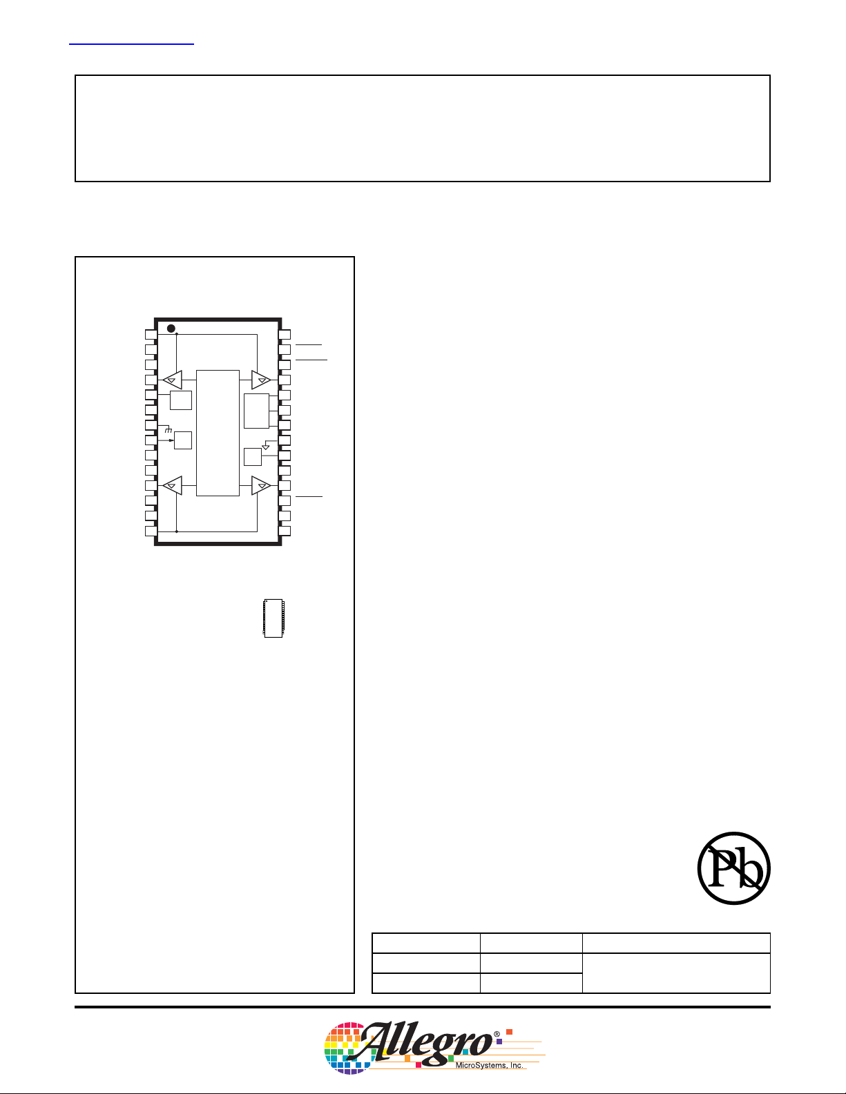
Package LP, 28-pin TSSOP
with Exposed Thermal Pad
1
SENSE1
2
HOME
3
DIR
4
OUT1A
5
PFD
RC1
AGND
REF
RC2
VDD
OUT2A
MS2
MS1
SENSE2
PWM
Timer
6
7
8
9
10
11
12
13
14
AGND and PGND must be
connected together externally.
÷8
Translator
and
Control
Logic
Approximate Scale 1:1
AB SO LUTE MAX I MUM RAT INGS
Load Supply Voltage,V
Output Current, I
OUT
Logic Supply Voltage, V
Logic Input Voltage Range, V
t
> 30 ns........................–0.3 V to VDD + 0.3 V
W
t
< 30 ns..............................–1 V to VDD + 1 V
W
Sense Voltage, V
SENSE
Reference Voltage, V
Package Power Dissipation, P
Operating Temperature Range
Ambient, T
, Range S ...................–20°C to 85°C
A
Junction Temperature, T
Storage Temperature, T
*
Output current rating may be limited by duty cycle,
ambient temperature, and heat sinking. Under any set of
conditions, do not exceed the specified current rating or a
junction temperature of 150°C.
...................................35 V
BB
...................................... ±2.5 A
...............................7.0 V
DD
IN
.......................................0.5 V
......................................V
REF
S
.................See page 5
D
J(MAX)
.................... –55°C to 150°C
28
VBB1
27
SLEEP
26
ENABLE
25
OUT1B
24
23
22
21
20
19
18
17
16
15
CP2
CP1
VCP
PGND
VREG
STEP
OUT2B
RESET
SR
VBB2
Charge
Pump
Reg
.....................150°C
A3979
The A3979 is a complete microstepping motor driver with built-in
translator, designed as a pin-compatible replacement for the successful
A3977, with enhanced microstepping (1/16 step) precision. It is designed
to operate bipolar stepper motors in full-, half-, quarter-, and sixteenthstep modes, with an output drive capacity of up to 35 V and ±2.5 A. The
A3979 includes a fixed off-time current regulator that has the ability
to operate in Slow, Fast, or Mixed decay modes. This current-decay
control scheme results in reduced audible motor noise, increased step
accuracy, and reduced power dissipation.
The translator is the key to the easy implementation of the A3979. It
allows the simple input of one pulse on the STEP pin to drive the motor
one microstep, which can be either a full step, half, quarter, or sixteenth,
depending on the setting of the MS1 and MS2 logic inputs. There are no
phase-sequence tables, high-frequency control lines, or complex interfaces to program. The A3979 interface is an ideal fit for applications
where a complex microprocessor is unavailable or is overburdened.
Internal synchronous-rectification control circuitry is provided to
improve power dissipation during PWM operation. Internal circuit
protection includes: thermal shutdown with hysteresis, UVLO (undervoltage lockout), and crossover-current protection. Special power-on
sequencing is not required.
The A3979 is supplied in a low-profile (maximum height ≤ 1.20 mm),
28-pin TSSOP with exposed thermal pad. The package is available in a
lead (Pb) free version, with 100% matte tin leadframe plating.
*
FEATURES
±2.5 A, 35 V output rating
Low R
Automatic current decay mode detection/selection
3.0 to 5.5 V logic supply voltage range
DD
Slow, Fast or Mixed current decay modes
Home output
Synchronous rectification for low power dissipation
Internal UVLO and thermal shutdown circuitry
Crossover-current protection
Use the following complete part number when ordering:
Part Number Pb-free Ambient, TA (°C)
A3979SLP –
A3979SLP-T Yes
outputs: 0.28 Ω source, 0.22 Ω sink, typical
DS(On)
–20 to 85
26184.23
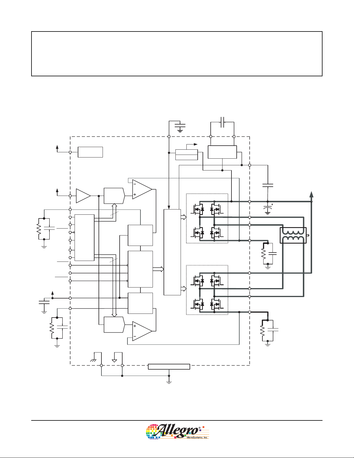
DMOS Microstepping Driver with Translator
Functional Block Diagram
A3979
R
T1
Logic
Supply
Reference
Supply
STEP
C
T1
RESET
HOME
SLEEP
ENABLE
V
PFD
0.1 µF
VDD
REF
RC1
DIR
MS1
MS2
SR
PFD
RC2
UVLO and
Fault
Translator
Charge
Pump
0.22 µF
CP1
VCP
VBB1
OUT1A
OUT1B
SENSE1
VBB2
OUT2A
OUT2B
SENSE2
R
0.22 µF
S1
>47 µF
C
S1
Load
Supply
0.22 µF
VREG
Regulator
Bandgap
DAC
4
PWM Timer:
PWM Latch
Blanking
Mixed Decay
Gate
Drive
4
Control
Logic
PWM Timer:
PWM Latch
Blanking
Mixed Decay
CP2
2 V
DMOS Full Bridge
DMOS Full Bridge
26184.23
C
R
T2
T2
AGND PGND
DAC
Exposed Thermal Pad
C
R
S2
S2
(Required)
Allegro MicroSystems, Inc.
115 Northeast Cutoff, Box 15036
Worcester, Massachusetts 01615-0036 (508) 853-5000
www.allegromicro.com
2
A3979
DMOS Microstepping Driver with Translator
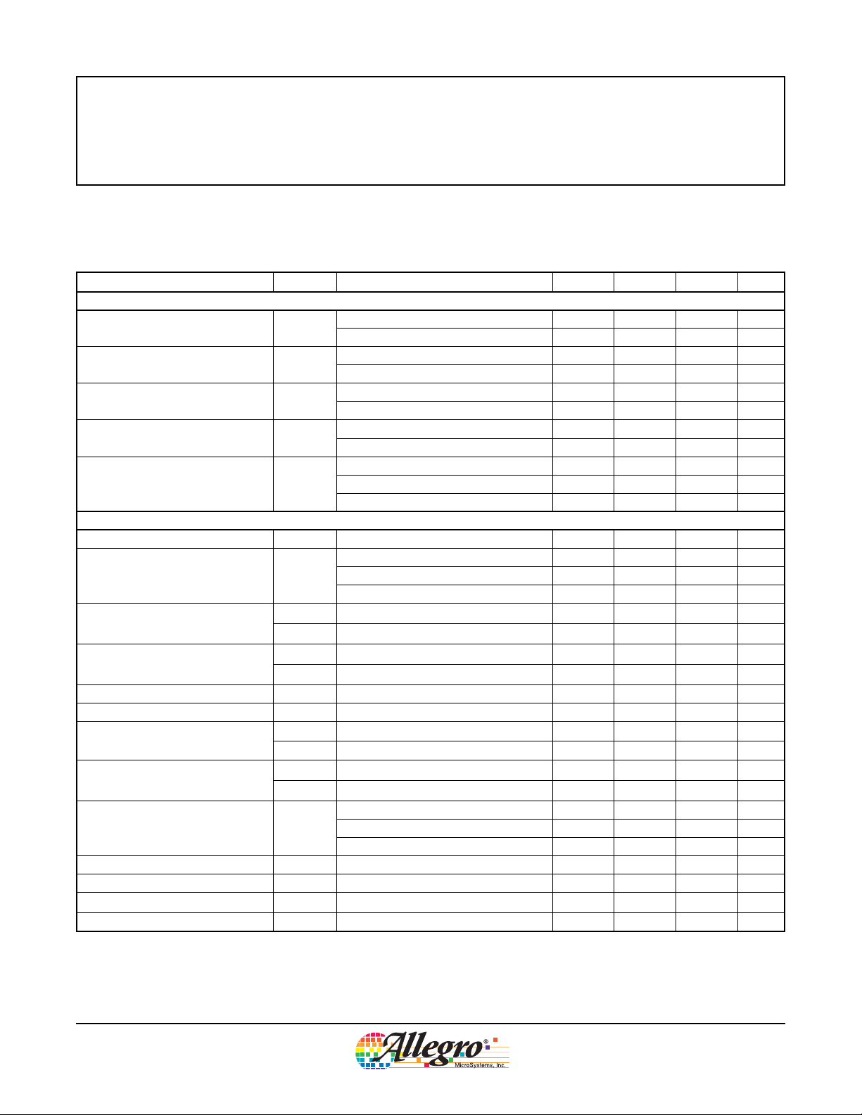
ELECTRICAL CHARACTERISTICS at T
Characteristics Symbol Test Conditions Min.
Output Drivers
Load Supply Voltage Range V
Output Leakage Current
2
Output On Resistance R
Body Diode Forward Voltage V
Motor Supply Current I
Control Logic
Logic Supply Voltage Range V
Logic Supply Current I
Logic Input Voltage
Logic Input Current
2
Reference Input Voltage Range V
Reference Input Current I
HOME Output Voltage
Mixed Decay Mode Trip Point
Gain (G
m
) Error
3
STEP Pulse Width t
Blank Time t
Fixed Off-Time
Crossover Dead Time t
BB
I
DSS
DS(On)
F
BB
DD
DD
V
IN(1)
V
IN(0)
I
IN(1)
I
IN(0)
REF
REF
V
HOME(1)
V
HOME(0)
V
PFDH
V
PFDL
E
G
W
BLANKRT
t
OFF
DT
= 25°C, V
A
= 35 V, VDD = 3.0 to 5.5 V (unless otherwise noted)
BB
1
Typ.
Max. Units
Operating 8 – 35 V
During Sleep mode 0 – 35 V
V
= V
OUT
V
OUT
Source driver, I
Source driver, I
BB
= 0 V – <1.0 –20 μA
= –2.5 A – 0.28 0.335 Ω
OUT
= 2.5 A – 0.22 0.265 Ω
OUT
– <1.0 20 μA
Source diode, IF = –2.5 A – – 1.4 V
Sink diode, IF = 2.5 A – – 1.4 V
f
< 50 kHz – – 8.0 mA
PWM
Operating, outputs disabled – – 6.0 mA
Sleep mode – – 20 μA
Operating 3.0 5.0 5.5 V
f
< 50 kHz – – 12 mA
PWM
Outputs off – – 10 mA
Sleep mode – – 20 μA
0.7× V
DD
––
VIN = 0.7 × V
V
= 0.3 × V
IN
DD
DD
–20 <1.0 20 μA
–20 <1.0 20 μA
Operating 0 – V
––V
0.3
×V
DD
DD
–0±3μA
I
I
V
V
V
= –200 μA
HOME(1)
= 200 μA––
HOME(0)
0.7
× V
DD
–
–
= 2 V, Phase Current = 38.27% – – ±10 %
REF
= 2 V, Phase Current = 70.71% – – ±5.0 %
REF
= 2 V, Phase Current = 100.00% – – ±5.0 %
REF
––V
0.3
× V
0.6
0.21
×V
×V
DD
DD
–V
–V
DD
1––μs
= 56 kΩ, CT = 680 pF 700 950 1200 ns
RT = 56 kΩ, CT = 680 pF 30 38 46 μs
Synchronous rectification enabled 100 475 800 ns
V
V
V
Continued on the next page...
26184.23
Allegro MicroSystems, Inc.
115 Northeast Cutoff, Box 15036
Worcester, Massachusetts 01615-0036 (508) 853-5000
www.allegromicro.com
3
A3979
DMOS Microstepping Driver with Translator
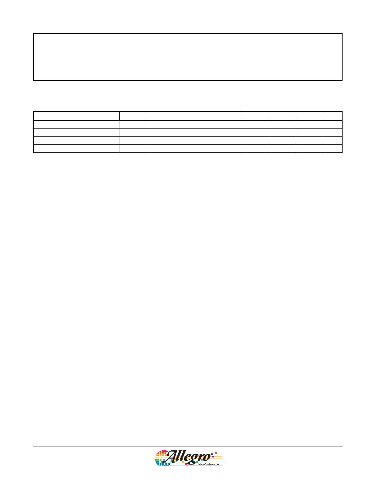
ELECTRICAL CHARACTERISTICS, continued at T
= 25°C, V
A
Characteristics Symbol Test Conditions Min.
Thermal Shutdown Temperature T
Thermal Shutdown Hysteresis T
UVLO Enable Threshold V
UVLO Hysteresis V
1
Typical data are for initial design estimations only, and assume optimum manufacturing and application conditions. Performance may vary for
individual units, within the specified maximum and minimum limits.
2
Negative current is defined as coming out of (sourcing from) the specified device pin.
3
EG = ( [ V
REF
/ 8] – V
SENSE
) / ( V
REF
/ 8 ).
JSD
JSDHYS
UVLO
UVLOHYS
Increasing VDD 2.45 2.7 2.95 V
= 35 V, VDD = 3.0 to 5.5 V (unless otherwise noted)
BB
1
Typ.
Max. Units
– 165 – °C
–15–°C
0.05 0.10 – V
26184.23
Allegro MicroSystems, Inc.
115 Northeast Cutoff, Box 15036
Worcester, Massachusetts 01615-0036 (508) 853-5000
www.allegromicro.com
4
A3979
DMOS Microstepping Driver with Translator
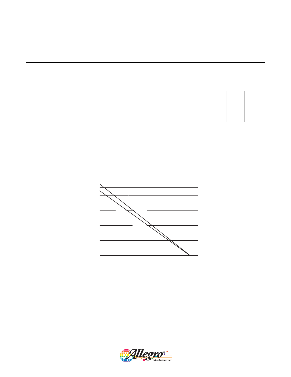
THERMAL CHARACTERISTICS may require derating at maximum conditions, see application information
Characteristic Symbol Test Conditions* Value Units
Two-layer PCB with 3.8 in.2 of copper area on each side
Package Thermal Resistance R
θJA
connected with thermal vias and to device exposed pad
High-K PCB (multilayer with significant copper areas,
based on JEDEC standard)
*Additional thermal information available on Allegro Web site.
32 ºC/W
28 ºC/W
Maximum Power Dissipation, P
5.0
4.5
(W)
D
Power Dissipation, P
4.0
3.5
3.0
2.5
2.0
1.5
1.0
0.5
0.0
High-K PCB
(R
θJA
= 28 ºC/W)
2-Layer PCB with 3.8 in
(R
θJA
= 32 ºC/W)
2
copper per side
20 40 60 80 100 120 140 160
Temperature (°C)
D(max)
26184.23
Allegro MicroSystems, Inc.
115 Northeast Cutoff, Box 15036
Worcester, Massachusetts 01615-0036 (508) 853-5000
www.allegromicro.com
5

DMOS Microstepping Driver with Translator
Timing Requirements
(T
= +25°C, VDD = 5 V, Logic Levels are VDD and Ground)
A
A3979
STEP
MS1/MS2/
DIR/RESET
SLEEP
50%
C D
B
A
E
A. Minimum Command Active Time
Before Step Pulse (Data Set-Up Time) ..... 200 ns
B. Minimum Command Active Time
After Step Pulse (Data Hold Time)............ 200 ns
C. Minimum STEP Pulse Width ...................... 1.0 μs
D. Minimum STEP Low Time ......................... 1.0 μs
Dwg. WP-042
26184.23
E. Maximum Wake-Up Time ......................... 1.0 ms
Figure 1. Logic Interface Timing Diagram
Table 1. Microstep Resolution Truth Table
MS1 MS2 Microstep Resolution Excitation Mode
L L Full Step 2 Phase
H L Half Step 1-2 Phase
L H Quarter Step W1-2 Phase
H H Sixteenth Step 4W1-2 Phase
Allegro MicroSystems, Inc.
115 Northeast Cutoff, Box 15036
Worcester, Massachusetts 01615-0036 (508) 853-5000
www.allegromicro.com
6

A3979
DMOS Microstepping Driver with Translator
Functional Description
Functional Description
Device Operation. The A3979 is a complete micro-
stepping motor driver with a built-in translator for easy
operation with minimal control lines. It is designed to
operate bipolar stepper motors in full-, half-, quarter-, and
sixteenth-step modes. The currents in each of the two output
full-bridges (all of the N-channel MOSFETs) are regulated
with fixed off-time PMW (pulse width modulated) control
circuitry. At each step, the current for each full-bridge is
set by the value of its external current-sense resistor (R
or RS2), a reference voltage (V
), and the output voltage
REF
S1
of its DAC (which in turn is controlled by the output of the
translator).
At power-on or reset, the translator sets the DACs and the
phase current polarity to the initial Home state (shown in
figures 2 through 5), and the current regulator to Mixed
decay mode for both phases. When a step command signal
occurs on the STEP input, the translator automatically
sequences the DACs to the next level and current polarity.
(See table 2 for the current-level sequence.) The microstep
resolution is set by the combined effect of inputs MS1 and
MS2, as shown in table 1.
While stepping is occurring, if the next output level of the
DACs is lower than the immediately preceeding output
level, then the decay mode (Fast, Slow, or Mixed) for the
active full bridge is set by the PFD input. If the next DAC
output level is higher than or equal to the preceeding level,
then the decay mode for that full bridge will be Slow decay.
This automatic current-decay selection improves microstepping performance by reducing the distortion of the current
waveform due to back EMF of the motor.
RESET Input ( ¯R¯ ¯E¯ ¯S¯ ¯E¯ ¯T¯ ). The ¯R¯ ¯E¯ ¯S¯ ¯E¯ ¯T¯ input (active
low) sets the translator to a predefined Home state (shown
in figures 2 through 5), and turns off all of the DMOS outputs. The HOME output goes low and all STEP inputs are
ignored until the ¯R¯ ¯E¯ ¯S¯ ¯E¯ ¯T¯
input is set to high.
Home Output (HOME). The HOME output is a logic
output indicator of the initial state of the translator. At
power-on, the translator is reset to the Home state (shown in
figures 2 through 5).
Step Input (STEP). A low-to-high transition on the
STEP input sequences the translator and advances the motor
one increment. The translator controls the input to the DACs
and the direction of current flow in each winding. The size
of the increment is determined by the combined state of
inputs MS1 and MS2 (see table 1).
Microstep Select (MS1 and MS2). The input on
terminals MS1 and MS2 selects the microstepping format,
as shown in table 1. Any changes made to these inputs do not
take effect until the next rising edge of a step command signal
on the STEP input.
Direction Input (DIR). The state of the DIR input deter-
mines the direction of rotation of the motor. Any changes
made to this input does not take effect until the next rising
edge of a step command signal on the STEP input.
Internal PWM Current Control. Each full bridge is
controlled by a fixed–off-time PWM current-control circuit
that limits the load current to a desired value, I
a diagonal pair of source and sink MOS outputs are enabled
and current flows through the motor winding and the current
sense resistor, R
. When the voltage across R
Sx
DAC output voltage, the current-sense comparator resets the
PWM latch. The latch then turns off either the source MOSFETs (when in Slow decay mode) or the sink and source
MOSFETs (when in Fast or Mixed decay mode).
The maximum value of current limiting is set by the selection of R
and the voltage at the V
S
input with a transcon-
REF
ductance function approximated by:
I
max = V
TRIP
The DAC output reduces the V
/8R
REF
REF
S
output to the cur-
rent-sense comparator in precise steps (see table 2 for
% I
max at each step).
TRIP
= (% I
I
TRIP
max/100) I
TRIP
TRIP
It is critical that the maximum rating (0.5 V) on either the
SENSE1 and SENSE2 pins is not exceeded. For full stepping, V
because the peak sense value is 0.707 × V
modes, V
can be applied up to the maximum rating of VDD
REF
REF
should not exceed 4 V.
REF
. Initially,
TRIP
equals the
Sx
max
/ 8. In all other
26184.23
Allegro MicroSystems, Inc.
115 Northeast Cutoff, Box 15036
Worcester, Massachusetts 01615-0036 (508) 853-5000
www.allegromicro.com
7

A3979
DMOS Microstepping Driver with Translator
Fixed Off-Time. The internal PWM current-control cir-
cuitry uses a one-shot timer to control the duration of time
that the MOSFETs remain off. The one shot off-time, t
is determined by the selection of external resistors, R
capacitors, C
ground. The off-time, over a range of values of C
to 1500 pF and R
, connected from each RCx timing terminal to
Tx
= 12 kΩ to 100 kΩ is approximated by:
T
t
= RTCT
OFF
= 470 pF
T
OFF
Tx
,
, and
RC Blanking. In addition to the fixed off-time of the
PWM control circuit, the CTx component sets the comparator blanking time. This function blanks the output of the
current-sense comparators when the outputs are switched
by the internal current-control circuitry. The comparator
outputs are blanked to prevent false overcurrent detection
due to reverse recovery currents of the clamp diodes, or to
switching transients related to the capacitance of the load.
The blank time t
can be approximated by:
BLANK
t
BLANK
= 1400C
T
Charge Pump (CP1 and CP2). The charge pump is
used to generate a gate supply greater than that of VBB for
driving the source-side DMOS gates. A 0.22 μF ceramic
capacitor should be connected between CP1 and CP2 for
pumping purposes. In addition, a 0.22 μF ceramic capacitor
is required between VCP and VBB, to act as a reservoir for
operating the high-side DMOS gates.
V
(VREG). This internally-generated voltage is used to
REG
operate the sink-side DMOS outputs. The VREG pin must
be decoupled with a 0.22 μF capacitor to ground. V
REG
is
internally monitored, and in the case of a fault condition, the
DMOS outputs of the device are disabled.
Enable Input (¯E¯ ¯N¯ ¯A¯ ¯B¯ ¯L¯ ¯E¯ ). This active-low input
enables all of the DMOS outputs. When set to a logic high,
the outputs are disabled. The inputs to the translator (STEP,
DIR, MS1, and MS2), all remain active, independent of the
¯E¯ ¯N¯ ¯A¯ ¯B¯ ¯L¯ ¯E¯ input state.
Shutdown. During normal operation, in the event of a
fault, such as overtemperature (excess T
) or an undervolt-
J
age on VCP, the outputs of the device are disabled until the
fault condition is removed.
At power up, and in the event of low V
, the undervoltage
DD
lockout (UVLO) circuit disables the drivers and resets the
translator to the Home state.
Sleep Mode ( ¯S¯ ¯L¯ ¯E¯ ¯E¯ ¯P¯ ). This active-low control input
is used to minimize power consumption when the motor is
not in use. It disables much of the internal circuitry including the output DMOS FETs, current regulator, and charge
pump. Setting this to a logic high allows normal operation,
as well as start-up (at which time the A3979 drives the
motor to the Home microstep position). When bringing the
device out of Sleep mode, in order to allow the charge pump
(gate drive) to stabilize, provide a delay of 1 ms before issuing a step command signal on the STEP input.
Percent Fast Decay Input (PFD). When a STEP
input signal commands a lower output current than the
previous step, it switches the output current decay to either
Slow, Fast, or Mixed decay mode, depending on the voltage
level at the PFD input. If the voltage at the PFD input is
greater than 0.6 × V
If the voltage on the PFD input is less than 0.21 × VDD , then
Fast decay mode is selected. Mixed decay mode is selected
when V
is between these two levels, as described in
PFD
the next section. This terminal should be decoupled with a
0.1 μF capacitor.
Mixed Decay Operation. If the voltage on the PFD input
is between 0.6 × V
in Mixed decay mode, as determined by the step sequence
(shown in figures 2 through 5). As the trip point is reached,
the device goes into Fast decay mode until the voltage
on the RCx terminal decays to the same level as voltage
applied to the PFD terminal. The time that the device operates in fast decay is approximated by:
tFD = RTCTln (0.6VDD/V
After this Fast decay portion, the device switches to Slow
decay mode for the remainder of the fixed off-time period.
, then Slow decay mode is selected.
DD
and 0.21 × VDD , the bridge operates
DD
)
PFD
26184.23
Allegro MicroSystems, Inc.
115 Northeast Cutoff, Box 15036
Worcester, Massachusetts 01615-0036 (508) 853-5000
www.allegromicro.com
8

A3979
DMOS Microstepping Driver with Translator
Synchronous Rectification. When a PWM off-
cycle is triggered by an internal fixed–off-time cycle, load
current recirculates according to the decay mode selected
by the control logic. The A3979 synchronous rectification
feature turns on the appropriate MOSFETs during the decay
of the current, and effectively shorts out the body diodes
with the low R
driver. This reduces power dissipation
DS(On)
significantly and eliminates the need for external Schottky
diodes for most applications. The synchronous rectification
can be set to either Active mode or Disabled mode:
Applications Information
Layout. The printed circuit board on which the device is
mounted should have a heavy ground plane. For optimum
electrical and thermal performance, the A3979 should be
soldered directly onto the board.
The load supply terminals, VBBx, should be decoupled with
an electrolytic capacitor (>47 μF is recommended), placed
as close to the device as possible.
To avoid problems due to capacitive coupling of the high
dv / dt switching transients, route the bridge-output traces
away from the sensitive logic-input traces.
Always drive the logic inputs with a low source impedance
to increase noise immunity.
Grounding. The AGND (analog ground) terminal and the
PGND (power ground) terminal must be connected together
externally.
All ground lines should be connected together and be as
short as possible. A star ground system, centered under the
device, is an optimum design.
The copper ground plane located under the exposed thermal
pad is typically used as the star ground.
• Active Mode. When the SR input is logic low, Active
mode is enabled and synchronous rectification can occur.
This mode prevents reversal of the load current by turning
off synchronous rectification when a zero current level is
detected. This prevents the motor winding from conducting in the reverse direction.
• Disabled Mode. When the SR input is logic high, syn-
chronous rectification is disabled. This mode is typically used when external diodes are required to transfer
power dissipation from the A3979 package to the external
diodes.
Current Sensing. To minimize inaccuracies caused by
ground-trace IR drops in sensing the output current level,
the current-sense resistors, R
ground return to the star ground of the device. This path
should be as short as possible.
For low-value sense resistors, the IR drops in the printed circuit board sense resistor traces can be significant and should
be taken into account.
The use of sockets should be avoided as they can introduce
variation in R
due to their contact resistance.
Sx
Allegro MicroSystems recommends a value of R
RS = 0.5/I
Thermal Protection.
all drivers when the junction temperature reaches 165°C,
typical. It is intended only to protect the device from failures
due to excessive junction temperatures and should not imply
that output short circuits are permitted. Thermal shutdown
has a hysteresis of approximately 15°C.
, should have an independent
Sx
given by
S
max
TRIP
This internal circuitry turns off
26184.23
Allegro MicroSystems, Inc.
115 Northeast Cutoff, Box 15036
Worcester, Massachusetts 01615-0036 (508) 853-5000
www.allegromicro.com
9

Home Microstep Position
Home Microstep Position
100.00
70.71
–70.71
0.00
–100.00
100.00
70.71
–70.71
0.00
–100.00
Phase 2
I
OUT2B
Direction = H
(%)
Phase 1
I
OUT1A
Direction = H
(%)
Slow
Mixed
Slow
Mixed
Slow
Mixed
Mixed
Slow
Mixed
Slow
Mixed
Slow
Slow
STEP Input
HOME Output
STEP Input
HOME Output
A3979
DMOS Microstepping Driver with Translator
100.00
70.71
Phase 1
I
OUT1A
0.00
Slow
Direction = H
(%)
–70.71
–100.00
100.00
70.71
Home Microstep Position
Phase 2
I
OUT2A
(%)
0.00
Slow
–70.71
–100.00
Direction = H
STEP Input
HOME Output
100.00
92.39
70.71
(%)
(%)
–38.27
–70.71
–92.39
–100.00
100.00
–38.27
–70.71
–92.39
–100.00
38.27
0.00
92.39
70.71
38.27
0.00
Slow
Slow
Phase 1
I
OUT1A
Direction = H
Phase 2
I
Figure 4. Decay Modes for Quarter-Step Increments
Direction = H
OUT2B
26184.23
Home Microstep Position
Mixed
Home Microstep Position
Slow
Figure 3. Decay Modes for Half-Step IncrementsFigure 2. Decay Mode for Full-Step Increments
Slow
Mixed
Mixed
Slow
Slow
MixedMixed
Allegro MicroSystems, Inc.
115 Northeast Cutoff, Box 15036
Worcester, Massachusetts 01615-0036 (508) 853-5000
www.allegromicro.com
10

DMOS Microstepping Driver with Translator
STEP Input
HOME Output
Phase 1
Direction = H
Phase 2
Direction = H
Figure 5. Decay Modes for Sixteenth-Step Increments
26184.23
I
OUT1A
(%)
I
OUT2B
(%)
100.00
95.69
88.19
83.15
77.30
70.71
63.44
55.56
47.14
38.27
29.03
19.51
0.00
–9.8
–19.51
–29.03
–38.27
–47.14
–55.56
–63.44
–70.71
–77.30
–83.15
–88.19
–95.69
–100.00
100.00
95.69
88.19
83.15
77.30
70.71
63.44
55.56
47.14
38.27
29.03
19.51
0.00
–9.8
–19.51
–29.03
–38.27
–47.14
–55.56
–63.44
–70.71
–77.30
–83.15
–88.19
–95.69
–100.00
9.8
Slow
9.8
Mixed
MixedSlow MixedSlow
Home Microstep Position
MixedSlow Slow
A3979
Allegro MicroSystems, Inc.
115 Northeast Cutoff, Box 15036
Worcester, Massachusetts 01615-0036 (508) 853-5000
www.allegromicro.com
11

DMOS Microstepping Driver with Translator
Table 2. Step Sequencing Settings
Home microstep position at Step Angle 45º; DIR = H; 360° = 4 full steps
A3979
Full
Step
#
Half
Step
#
1/4
Step
#
1/16
Step
#
Phase 1
Current
[% I
tripMax
(%)
Phase 2
]
[% I
Current
tripMax
(%)
]
Step
Angle
(º)
Full
Step
#
Half
Step
#
1/4
Step
#
1/16
Step
#
Phase 1
Current
[% I
tripMax
(%)
Phase 2
Current
[% I
]
tripMax
(%)
]
Angle
1 1 1 100.00 0.00 0.0 5 9 33 –100.00 0.00 180.0
2 99.52 9.80 5.6 34 –99.52 –9.80 185.6
3 98.08 19.51 11.3 35 –98.08 –19.51 191.3
4 95.69 29.03 16.9 36 –95.69 –29.03 196.9
2 5 92.39 38.27 22.5 10 37 –92.39 –38.27 202.5
6 88.19 47.14 28.1 38 –88.19 –47.14 208.1
7 83.15 55.56 33.8 39 –83.15 –55.56 213.8
8 77.30 63.44 39.4 40 –77.30 –63.44 219.4
1 2 3 9 70.71 70.71 45.0 3 6 11 41 –70.71 –70.71 225.0
10 63.44 77.30 50.6 42 –63.44 –77.30 230.6
11 55.56 83.15 56.3 43 –55.56 –83.15 236.3
12 47.14 88.19 61.9 44 –47.14 –88.19 241.9
4 13 38.27 92.39 67.5 12 45 –38.27 –92.39 247.5
14 29.03 95.69 73.1 46 –29.03 –95.69 253.1
15 19.51 98.08 78.8 47 –19.51 –98.08 258.8
16 9.80 99.52 84.4 48 –9.80 –99.52 264.4
3 5 17 0.00 100.00 90.0 7 13 49 0.00 –100.00 270.0
18 –9.80 99.52 95.6 50 9.80 –99.52 275.6
19 –19.51 98.08 101.3 51 19.51 –98.08 281.3
20 –29.03 95.69 106.9 52 29.03 –95.69 286.9
6 21 –38.27 92.39 112.5 14 53 38.27 –92.39 292.5
22 –47.14 88.19 118.1 54 47.14 –88.19 298.1
23 –55.56 83.15 123.8 55 55.56 –83.15 303.8
24 –63.44 77.30 129.4 56 63.44 –77.30 309.4
2 4 7 25 –70.71 70.71 135.0 4 8 15 57 70.71 –70.71 315.0
26 –77.30 63.44 140.6 58 77.30 –63.44 320.6
27 –83.15 55.56 146.3 59 83.15 –55.56 326.3
28 –88.19 47.14 151.9 60 88.19 –47.14 331.9
8 29 –92.39 38.27 157.5 16 61 92.39 –38.27 337.5
30 –95.69 29.03 163.1 62 95.69 –29.03 343.1
31 –98.08 19.51 168.8 63 98.08 –19.51 348.8
32 –99.52 9.80 174.4 64 99.52 –9.80 354.4
Step
(º)
26184.23
Allegro MicroSystems, Inc.
115 Northeast Cutoff, Box 15036
Worcester, Massachusetts 01615-0036 (508) 853-5000
www.allegromicro.com
12

DMOS Microstepping Driver with Translator
Terminal List Table
Number Name Description
1 SENSE1 Sense resistor for Bridge 1
2 HOME Logic Output
3 DIR Logic input
4 OUT1A Output A for Bridge 1
5 PFD Mixed decay setting
6 RC1 Analog input for fixed off-time for Bridge 1
7 AGND Analog Ground
8 REF Current trip reference voltage input
9 RC2 Analog input for fixed off-time for Bridge 2
10 VDD Logic supply
11 OUT2A Output A for Bridge 2
12 MS2 Logic input
13 MS1 Logic input
14 SENSE2 Sense resistor for Bridge 2
15 VBB2 Load supply for Bridge 2
16 SR Logic input
17 ¯R¯ ¯E¯ ¯S¯ ¯E¯ ¯T¯ Logic input
18 OUT2B Output B for Bridge 2
19 STEP Logic input
20 VREG Regulator decoupling
21 PGND Power Ground
22 VCP Reservoir capacitor
23 CP1 Charge pump capacitor 1
24 CP2 Charge pump capacitor 2
25 1OUT1B Output B for Bridge 1
26 ¯E¯ ¯N¯ ¯A¯ ¯B¯ ¯L¯ ¯E¯ Logic input
27 ¯S¯ ¯L¯ ¯E¯ ¯E¯ ¯P¯ Logic input
28 VBB1 Load supply for Bridge 1
A3979
26184.23
Allegro MicroSystems, Inc.
115 Northeast Cutoff, Box 15036
Worcester, Massachusetts 01615-0036 (508) 853-5000
www.allegromicro.com
13

LP Package, 28-Pin TSSOP with Exposed Thermal Pad
Preliminary dimensions, for reference only
Dimensions in millimeters
U.S. Customary dimensions (in.) in brackets, for reference only
(reference JEDEC MO-153 AET)
Dimensions exclusive of mold flash, gate burrs, and dambar protrusions
Exact case and lead configuration at supplier discretion within limits shown
A
Terminal #1 mark area
B
Exposed thermal pad (bottom surface)
28X
28X
0.10 [.004]
M C A B
0.30
0.19
DMOS Microstepping Driver with Translator
9.8
.386
9.6
28
A
21
C0.10 [.004]
.012
.007
.378
5
.200
NOM
0.65 .026
B
A
3
NOM
.118
0.150.006
4.5
4.3
SEATING
PLANE
1.20
MAX
.000
B
.177
.169
6.6
.260
6.2
.244
C
.047
A3979
8º
0º
0.20
.008
0.09
.004
0.75
.030
0.45
.018
1
.039
REF
0.25 .010
SEATING PLANE
GAUGE PLANE
The products described here are manufactured under one or more U.S. patents or U.S. patents pending.
Allegro MicroSystems, Inc. reserves the right to make, from time to time, such de par tures from the detail spec i fi ca tions as may be
required to permit improvements in the per for mance, reliability, or manufacturability of its products. Before placing an order, the user is
cautioned to verify that the information being relied upon is current.
®
Allegro
products are not authorized for use as critical components in life-support devices or sys tems without express written approval.
The in for ma tion in clud ed herein is believed to be ac cu rate and reliable. How ev er, Allegro MicroSystems, Inc. assumes no re spon si bil i ty
for its use; nor for any in fringe ment of patents or other rights of third parties which may result from its use.
Copyright©2005 AllegroMicrosystems, Inc.
26184.23
Allegro MicroSystems, Inc.
115 Northeast Cutoff, Box 15036
Worcester, Massachusetts 01615-0036 (508) 853-5000
www.allegromicro.com
14
 Loading...