

A3972
Dual DMOS Full-Bridge Microstepping PWM Motor Driver
Features and Benefits
▪ ±1.5 A, 50 V Continuous Output Rating
▪ Low R
▪ Optimized Microstepping via 6-Bit Linear DACs
▪ Programmable Mixed, Fast, and Slow Current-Decay
Modes
▪ 4 MHz Internal Oscillator for Digital Timing
▪ Serial-Interface Controls Chip Functions
▪ Synchronous Rectification for Low Power Dissipation
▪ Internal UVLO and Thermal Shutdown Circuitry
▪ Crossover-Current Protection
▪ Precision 2 V Reference
▪ Inputs Compatible with 3.3 or 5 V Control Signals
▪ Sleep and Idle Modes
DMOS Output Drivers
DS(on)
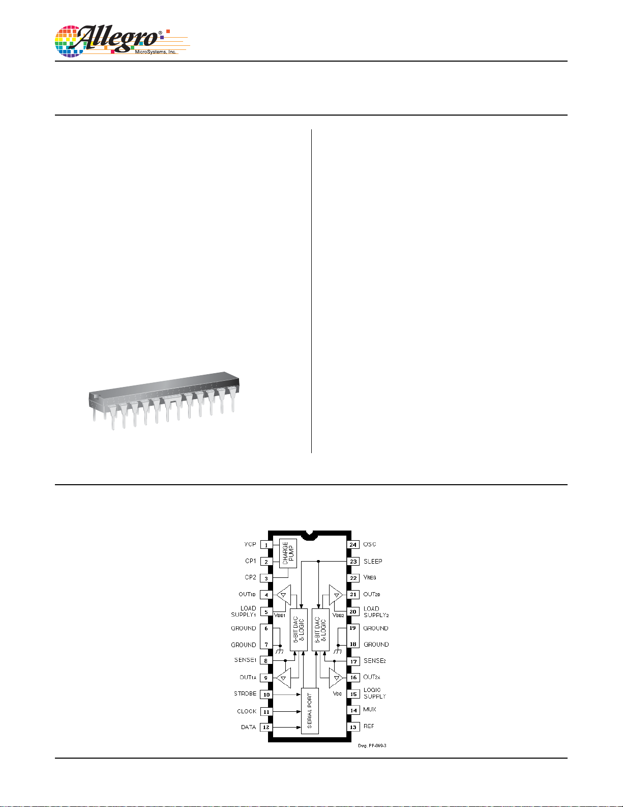
Package: 24-pin DIP with 4 fused leads
(suffix B)
Not to scale
Description
Designed for pulse-width modulated (PWM) current control
of bipolar microstepping stepper motors, the A3972 is capable
of continuous output currents to ±1.5 A and operating voltages
to 50 V. Internal fixed off-time PWM current-control timing
circuitry can be programmed via a serial interface to operate
in slow, fast, and mixed current-decay modes.
The desired load-current level is set via the serial port with
two 6-bit linear DACs in conjunction with a reference voltage.
The six bits of control allow maximum flexibility in torque
control for a variety of step methods, from microstepping to
full-step drive. Load current is set in 1.56% increments of the
maximum value.
Synchronous rectification circuitry allows the load current
to flow through the low R
during the current decay. This feature will eliminate the
need for external clamp diodes in most applications, saving
cost and external component count, while minimizing power
dissipation.
Internal circuit protection includes thermal shutdown with
hysteresis, transient-suppression diodes, and crossover-current
protection. Special power-up sequencing is not required.
The A3972SB is supplied in a 24-pin plastic DIP with two
batwing power tabs (suffix ‘B’). The power tabs are at ground
potential and need no electrical isolation. The device is lead
(Pb) free with 100% matte tin leadframe plating.
of the DMOS output driver
DS(on)
29319.33, Rev. D
Pin-out Diagram

Dual DMOS Full-Bridge
A3972
Microstepping PWM Motor Driver
Selection Guide
Part Number Packing
A3972SB-T 15 pieces/tube
Absolute Maximum Ratings
Characteristic Symbol Notes Rating Units
Load Supply Voltage V
Output Current* I
Logic Supply Voltage V
Logic Input Voltage Range V
Reference Voltage V
Sense Voltage (DC) V
Package Power Dissipation P
Operating Ambient Temperature T
Junction Temperature T
Storage Temperature T
*Output current rating may be limited by duty cycle, ambient temperature, and heat sinking. Under any set of conditions, do not exceed
the specifi ed current rating or a junction temperature of 150°C.
BB
OUT
DD
REF
stg
IN
S
D
A
J
Range S –20 to 85 ºC
50 V
±1.5 A
7.0 V
–0.3 to VDD + 0.3 V
3V
500 mV
3.1 W
150 ºC
–55 to 150 ºC
Allegro MicroSystems, Inc.
115 Northeast Cutoff
Worcester, Massachusetts 01615-0036 U.S.A.
1.508.853.5000; www.allegromicro.com
2
A3972
Dual DMOS Full-Bridge
Microstepping PWM Motor Driver
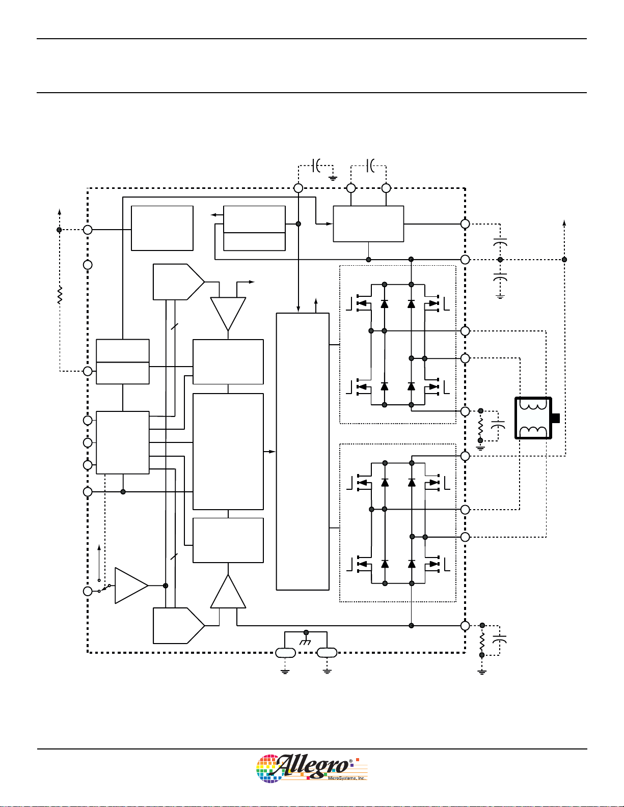
FUNCTIONAL BLOCK DIAGRAM
LOGIC
SUPPLY
CLOCK
DATA
STROBE
SLEEP
V
MUX
OSC
15
DD
14
24
11
12
10
23
OSCILATOR
OSC SELECT/
DIVIDER
SERIAL
PORT
2 V
UVLO AND
FAULT
DETECT
6-BIT
LINEAR
DAC
6
6
2 V
REGULATOR
BANDGAP
+-
PROGRAMMABLE
PWM TIMER
FIXED-OFF
BLANK
MIXED DECAY
CONTROL
LOGIC
PHASE 1/2
SYNC. RECT. MODE
SYNC. RECT. DISABLE
MODE 1/2
PROGRAMMABLE
PWM TIMER
FIXED-OFF
BLANK
MIXED DECAY
SENSE
1
V
22
GATE
DRIVE
0.22 μF
REG
V
CP
0.22 μF
3
CP1CP2
2
CHARGE PUMP
DMOS H-BRIDGE
DMOS H-BRIDGE
1
5
9
OUT
4
8
20
16
21
V
CP
V
BB1
OUT
1A
1B
SENSE
V
BB2
OUT
2A
OUT
2B
1
0.1 μF
0.22 μF
LOAD
SUPPLY
REF
13
Dwg. FP-050-1
BUFFER
6-BIT
LINEAR
DAC
+-
GROUND
6
18
7
19
Copyright © 2000, Allegro MicroSystems, Inc.
SENSE
17
Allegro MicroSystems, Inc.
115 Northeast Cutoff
Worcester, Massachusetts 01615-0036 U.S.A.
1.508.853.5000; www.allegromicro.com
2
0.1
μ
F
3

Dual DMOS Full-Bridge
A3972
Microstepping PWM Motor Driver
ELECTRICAL CHARACTERISTICS at TA = +25°C, VBB = 50 V, VDD = 5.0 V, VS = 0.5 V,
f
< 50 kHz (unless otherwise noted).
PWM
Limits
Characteristic Symbol Test Conditions Min. Typ. Max. Units
Load Supply Voltage Range VBB Operating 15 — 50 V
During sleep mode 0 — 50 V
Logic Supply Voltage Range V
Load Supply Current I
Operating 4.5 5.0 5.5 V
DD
f
BB
< 50 kHz — — 8.0 mA
PWM
Operating, outputs disabled — — 6.0 mA
Sleep or idle mode — — 20 μA
Logic Supply Current IDD f
< 50 kHz — — 12 mA
PWM
Outputs off — — 10 mA
Idle mode (D0 = 1, D18 = 0) — — 1.5 mA
Sleep mode — — 100 μA
Output Drivers
Output Leakage Current I
V
Output On Resistance r
Sink driver, I
Body Diode Forward Voltage V
V
DSS
DS(on)
F
OUT
OUT
Source driver, I
Source diode, IF = 1.5 A — — 1.2 V
Sink diode, IF = 1.5 A — — 1.2 V
= VBB — <1.0 50 μA
= 0 V — <-1.0 -50 μA
= –1.5 A — 0.5 0.55 Ω
OUT
= 1.5 A — 0.315 0.35 Ω
OUT
Control Logic
Logic Input Voltage V
V
Logic Input Current I
I
OSC Input Frequency Range f
2.0 — — V
IN(1)
— — 0.8 V
IN(0)
VIN = 2.0 V — <1.0 20 μA
IN(1)
V
IN(0)
Divide by one 2.5 — 6.0 MHz
OSC
= 0.8 V — <-2.0 -20 μA
IN
(D0 =1, D13 = 0, D14 = 1)
OSC Input Duty Cycle — 40 — 60 %
Input Hysterisis ΔVIN 0.20 — 0.40 V
continued next page ...
Allegro MicroSystems, Inc.
115 Northeast Cutoff
Worcester, Massachusetts 01615-0036 U.S.A.
1.508.853.5000; www.allegromicro.com
4

Dual DMOS Full-Bridge
A3972
Microstepping PWM Motor Driver
ELECTRICAL CHARACTERISTICS at TA = +25°C, VBB = 50 V, VDD = 5.0 V, VS = 0.5 V,
f
< 50 kHz (unless otherwise noted).
PWM
Limits
Characteristics Symbol Test Conditions Min. Typ. Max. Units
Control Logic (continued)
Internal Oscillator f
DAC Accuracy (total error) E
OSC
T
Reference Input Voltage Range V
Reference Buffer Offset V
Reference Divider Ratio V
REF(EXT)
OS
REF/VS
OSC shorted to ground 3.0 4.0 5.0 MHz
R
= 51 kΩ 3.4 4.0 4.6 MHz
OSC
Relative to DAC reference buffer
— ±1/2 — LSB
output, D0 = 0, D17 = 0
0.5 — 2.6 V
— ±10 — mV
D0 = 0, D18 = 0 — 8.0 — —
D0 = 0, D18 = 1 — 4.0 — —
Reference Input Current I
Internal Reference Voltage V
REF
REF(INT)
V
= 2.0 V — — ±0.5 μA
REF
1.94 2.0 2.06 V
Gain (Gm) Error (note 3) EG D0 = 0, D17 = 0,
D18 = 0, DAC = 63 — 0 ±6 %
D18 = 0, DAC = 31 — 0 ±9 %
D18 = 1, DAC = 63 — 0 ±6 %
D18 = 1, DAC = 15 — 0 ±10 %
Comparator Input Offset Voltage VIO V
= 0 V — ±5.0 — mV
REF
Propagation Delay Times tpd 50% to 90%:
PWM change to source on 500 800 1200 ns
PWM change to source off 50 150 350 ns
PWM change to sink on 500 800 1200 ns
PWM change to sink off 50 150 350 ns
Crossover Dead Time tdt 300 700 900 ns
Thermal Shutdown Temperature TJ — 165 — °C
Thermal Shutdown Hysteresis ΔTJ — 15 — °C
UVLO Enable Threshold V
UVLO Hysteresis ΔV
Increasing VDD 3.9 4.2 4.45 V
UVLO
0.05 0.10 — V
UVLO
NOTES: 1. Typical Data is for design information only.
2. Negative current is defi ned as coming out of (sourcing) the specifi ed device terminal.
3. EG = [(V
/Range) – VS]/(V
REF
/Range).
REF
Allegro MicroSystems, Inc.
115 Northeast Cutoff
Worcester, Massachusetts 01615-0036 U.S.A.
1.508.853.5000; www.allegromicro.com
5

A3972
Dual DMOS Full-Bridge
Microstepping PWM Motor Driver
FUNCTIONAL DESCRIPTION
Serial Interface. The A3972SB is controlled via a 3-wire
(clock, data, strobe) serial port. The programmable functions
allow maximum fl exibility in confi guring the PWM to the motor
drive requirements. The serial data is written as two
19-bit words: 1 bit to select the word and 18 bits of data. The
serial data is clocked in starting with D18.
Word 0 Bit Assignments
Bit Function
D0 Word select = 0
D1 Bridge 1, DAC, LSB
D2 Bridge 1, DAC, bit 2
D3 Bridge 1, DAC, bit 3
D4 Bridge 1, DAC, bit 4
D5 Bridge 1, DAC, bit 5
D6 Bridge 1, DAC, MSB
D7 Bridge 2, DAC, LSB
D8 Bridge 2, DAC, bit 2
D9 Bridge 2, DAC, bit 3
D10 Bridge 2, DAC, bit 4
D11 Bridge 2, DAC, bit 5
D12 Bridge 2, DAC, MSB
D13 Bridge 1 phase
D14 Bridge 2 phase
D15 Bridge 1 mode
D16 Bridge 2 mode
D17 REF select
D18 Range select
D1 – D6 Bridge 1 Linear DAC. Six-bit word sets desired
current level for Bridge 1. Setting all six bits to zero disables
Bridge 1, with all drivers off (See current regulation section of
functional description).
D7 – D12 Bridge 2 Linear DAC. Six-bit word sets desired
current level for Bridge 2. Setting all six bits to zero disables
Bridge 2, with all drivers off (See current regulation section of
functional description).
D13 Bridge 1 Phase. This bit controls the direction of output
current for Load 1.
D13 OUT1A OUT
1B
0 L H
1 H L
D14 Bridge 2 Phase. This bit controls the direction of output
current for Load 2.
D14 OUT2A OUT
2B
0 L H
1 H L
D15 Bridge 1 Mode.
D15 Mode
0 Mixed-decay
1 Slow-decay
D16 Bridge 2 Mode.
D16 Mode
0 Mixed-decay
1 Slow-decay
D17 REF Select. This bit determines the reference input for
the 6-bit linear DACs.
D17 Reference Voltage
0 Internal 2 V
1 External (3 V max)
D18 Gm Range Select. This bit determines the scaling factor
(4 or 8) used.
D18 Divider Load Current
0 1/8 I
1 1/4 I
TRIP
TRIP
= V
= V
DAC
DAC
/8R
/4R
S
S
continued next page ...
Allegro MicroSystems, Inc.
115 Northeast Cutoff
Worcester, Massachusetts 01615-0036 U.S.A.
1.508.853.5000; www.allegromicro.com
6

A3972
Dual DMOS Full-Bridge
Microstepping PWM Motor Driver
FUNCTIONAL DESCRIPTION (continued)
Word 1 Bit Assignments
Bit Function
D0 Word select = 1
D1 Blank-time LSB
D2 Blank-time MSB
D3 Off-time LSB
D4 Off-time bit 1
D5 Off-time bit 2
D6 Off-time bit 3
D7 Off-time MSB
D8 Fast-decay time LSB
D9 Fast-decay time bit 1
D10 Fast-decay time bit 2
D11 Fast-decay time MSB
D12 C0 oscillator control
D13 C1 oscillator control
D14 SR control bit 1
D15 SR control bit 2
D16 Reserved for testing
D17 Reserved for testing
D18 Idle mode
D1 – D2 Blank Time. These two bits set the blank time for
the current-sense comparator. When a source driver turns on, a
current spike occurs due to the reverse-recovery currents of the
clamp diodes and/or switching transients related to distributed
capacitance in the load. To prevent this current spike from er-
roneously resetting the source-enable latch, the sense comparator
is blanked. The blank timer runs after the off-time counter to
provide the programmable blanking function. The blank timer is
reset when PHASE is changed.
D2 D1 Time
0 0 4/f
0 1 6/f
1 0 8/f
1 1 12/f
OSC
OSC
OSC
OSC
D3 – D7 Fixed Off Time. These fi ve bits set the fi xed off-time
for the internal PWM control circuitry. Fixed off-time is defi ned
by:
t
= [(1 + N) x 8/f
off
OSC
] - 1/f
OSC
where N = 0….31
For example, with a master oscillator frequency of 4 MHz, the
fi xed off-time will be adjustable from 1.75 μs to 63.75 μs in
increments of 2 μs.
D8 – D11 Fast Decay Time. These four bits set the fast-
decay portion of fi xed off-time for the internal PWM control
circuitry. The fast-decay portion is defi ned by:
tfd = [(1 + N) x 8/f
OSC
] - 1/f
OSC
where N = 0….15
For example, with an oscillator frequency of 4 MHz, the fast-
decay time will be adjustable from 1.75 μs to 31.75 μs in increments of 2 μs. For t
> t
, the device will effectively operate
fd
off
in fast-decay mode.
D12 – D13 Oscillator Control. A 4 MHz internal oscillator
is used for the timing functions and charge-pump clock. If more
precise control is required, an external oscillator can be input
to the OSC terminal. To accommodate a wider range of system
clocks, an internal divider is provided to generate the desired
MO frequency according to the following table:
D13 D12 OSC
0 0 4 MHz internal clock
0 1 External clock
1 0 External clock/2
1 1 External clock/4
D14 – D15 Synchronous Rectifi cation.
D15 D14 Synchronous Rectifi er
0 0 Active
0 1 Disabled
1 0 Passive
1 1 Low side only
The different modes of operation are in the synchronous rectifi -
cation section of the functional description.
D16, D17. These bits are reserved for testing and should be
programmed to zero during normal operation.
D18 Idle Mode. The device can be placed in a low power
“idle” mode by writing a “0” to D18. The outputs will be dis-
abled, the charge pump will be turned off, and the device will
draw a lower load supply currrent. The undervoltage monitor
circuit will remain active. D18 should be programmed high for
1 ms before attempting to enable any output driver.
continued next page ...
Allegro MicroSystems, Inc.
115 Northeast Cutoff
Worcester, Massachusetts 01615-0036 U.S.A.
1.508.853.5000; www.allegromicro.com
7

A3972
Dual DMOS Full-Bridge
Microstepping PWM Motor Driver
FUNCTIONAL DESCRIPTION (continued)
V
. This internally generated supply voltage is used to run
REG
the sink-side DMOS outputs. V
is internally monitored and
REG
in the case of a fault condition, the outputs of the device are
disabled. The V
pin should be decoupled with a 0.22 μF
REG
capacitor to ground.
Current Regulation. The reference voltage can be set by ana-
log input to the REF terminal, or via the internal 2 V precision
reference. The choice of reference voltage and sense resistor set
the maximum trip current.
I
TRIPMAX
= V
/(Range x RS)
REF
Microstepping current levels are set according to the following
equations:
I
= V
TRIP
V
= [(1 + DAC) x V
DAC
/(Range x RS)
DAC
REF
]/64
where DAC input code equals 1 to 63 and Range is 4 or 8 as
selected by Word 0, D18. Programming the DAC input code to
zero disables the bridge, and results in minimum load current.
PWM Timer Function. The PWM timer is programmable via
the serial port to provide fi xed off-time PWM signals to the con-
trol block. In mixed-decay mode, the fi rst portion of the off time
operates in fast decay, until the fast-decay time count is reached,
followed by slow decay for the rest of the fi xed off-time period.
If the fast-decay time is set longer than the off-time, the device
effectively operates in fast-decay mode.
Oscillator. The PWM timer is based on an oscillator input,
typically 4 MHz. The A3972SB can be confi gured to select ei-
ther a 4 MHz internal oscillator or, if more precision is required,
an external clock can be connected to the OSC terminal. If an
external clock is used, three internal divider choices are select-
able via the serial port to allow fl exibility in choosing f
OSC
,
based on available system clocks. If the internal oscillator op-
tion is used, the absolute accuracy is dependent on the process
variation of resistance and capacitance. A precision resistor can
be connected from the OSC terminal to VDD to further improve
the tolerance. The frequency will be:
= 204 x 109/R
f
OSC
OSC
If the internal oscillator is used without the external resistor, the
OSC terminal should be connected to ground.
Shutdown. In the event of a fault due to excessive junction
temperature, or low voltage on V
CP
or V
, the outputs of the
REG
device are disabled until the fault condition is removed. At
power up, or in the event of low VDD, the UVLO circuit disables
the drivers and resets the data in the serial port to zeros.
Synchronous Rectifi cation. When a PWM off-cycle is
triggered, either by a bridge disable command or internal fi xed
off-time cycle, the load current will recirculate according to
the decay mode selected by the control logic. The A3972SB
synchronous rectifi cation feature will turn on the appropriate
MOSFET(s) during the current decay and effectively short out
the body diodes with the low r
driver. This will lower
DS(on)
power dissipation signifi cantly and can eliminate the need for
external Schottky diodes for most applications.
Four distinct modes of operation can be confi gured with the two
serial port control bits:
1. Active Mode. Prevents reversal of load current by turning
off synchronous rectifi cation when a zero current level is
detected.
2. Passive Mode. Allows reversal of current but will turn
off the synchronous rectifi er circuit if the load current inver-
sion ramps up to the current limit.
3. Disabled. MOSFET switching will not occur during load
recirculation. This setting would only be used with four
external clamp diodes per bridge.
4. Low Side Only. The low-side MOSFETs will switch on
during the off time to short out the current path through
the MOSFET body diode. With this setting, the high-side
MOSFETs will not synchronously rectify so four external
diodes from output to supply are recommended. This mode
is intended for use with high-power applications where it
is desired to save the expense of two external diodes per
bridge. In this mode, the sink-side MOSFETs are chopped
during the PWM off time. In all other cases, the source-side
MOSFETs are chopped in response to a PWM off com-
mand.
Sleep Mode. The input terminal SLEEP is dedicated to putting
the device into a minimum current draw mode. When pulled
low, the serial port will be reset to all zeros and all circuits will
be disabled.
continued next page ...
Allegro MicroSystems, Inc.
115 Northeast Cutoff
Worcester, Massachusetts 01615-0036 U.S.A.
1.508.853.5000; www.allegromicro.com
8

A3972
Dual DMOS Full-Bridge
Microstepping PWM Motor Driver
APPLICATIONS INFORMATION
Current Sensing. To minimize inaccuracies in sensing the
I
current level caused by ground-trace IR drops, the sense
PEAK
resistor should have an independent ground return to the ground
terminal of the device. For low-value sense resistors, the IR
drops in the sense resistor’s PCB traces can be signifi cant and
should be taken into account. The use of sockets should be
avoided as they can introduce variation in RS due to their contact
resistance.
Thermal Protection. Circuitry turns off all drivers when the
junction temperature reaches 165°C typically. It is intended
only to protect the device from failures due to excessive junction
temperature and should not imply that output short circuits are
permitted. Thermal shutdown has a hysteresis of approximately
15°C.
Serial Port Write Timing Operation. Data is clocked into
a shift register on the rising edge of CLOCK signal. Normally,
STROBE will be held high, and only will be brought low to
initiate a write cycle. The data is written MSB fi rst, followed
by the word-select bit. Refer to serial port diagram for timing
requirements.
SLEEP
H
Layout. The printed wiring board should use a heavy ground
plane. For optimum electrical and thermal performance, the
driver should be soldered directly onto the board. The ground
side of RS should have an individual path to the ground pin(s) of
the driver. This path should be as short as physically possible
and should not have any other components connected to it. The
load supply pin, VBB, should be decoupled with an electrolytic
capacitor (>47 μF is recommended) placed as close to the driver
as is possible.
STROBE
E
CLOCK
A
B
DATA
D18 D0
A. Minimum Data Setup Time ....................................... 15 ns
B. Minimum Data Hold Time ........................................ 10 ns
C. Minimum Setup Strobe to Clock Rising Edge ........150 ns
D. Minimum Clock High Pulse Width ...........................40 ns
E. Minimum Clock Low Pulse Width ............................ 40 ns
F. Minimum Setup Clock Rising Edge to Strobe ........... 50 ns
G. Minimum Strobe Pulse Width ................................. 150 ns
H. Minimum Setup Sleep to Strobe Falling ................... 50 μs
D17
F
Allegro MicroSystems, Inc.
115 Northeast Cutoff
Worcester, Massachusetts 01615-0036 U.S.A.
1.508.853.5000; www.allegromicro.com
GC D
Dwg. WP-038-1
9

A3972
Dual DMOS Full-Bridge
Microstepping PWM Motor Driver
B Package, 24-Pin DIP
1.185
24
0.010
A
0.005
0.250 0.430
2
1
All dimensions nominal, not for tooling use
0.210
0.130
0.100
0.060
0.018
(reference JEDEC MS-001 BE)
Dimensions in inches
Pins 6, 7, 18 and 19 internally fused
Dimensions exclusive of mold flash, gate burrs, and dambar protrusions
Exact case and lead configuration at supplier discretion within limits shown
A
Terminal #1 mark area
0.300
Copyright ©2000-2007, Allegro MicroSystems, Inc.
The products described here are manufactured under one or more U.S. patents or U.S. patents pending.
Allegro MicroSystems, Inc. reserves the right to make, from time to time, such de par tures from the detail spec i fi ca tions as may be required to per-
mit improvements in the per for mance, reliability, or manufacturability of its products. Before placing an order, the user is cautioned to verify that the
information being relied upon is current.
Allegro’s products are not to be used in life support devices or systems, if a failure of an Allegro product can reasonably be expected to cause the
failure of that life support device or system, or to affect the safety or effectiveness of that device or system.
The in for ma tion in clud ed herein is believed to be ac cu rate and reliable. How ev er, Allegro MicroSystems, Inc. assumes no re spon si bil i ty for its use;
nor for any in fringe ment of patents or other rights of third parties which may result from its use.
For the latest version of this document, visit our website:
www.allegromicro.com
Allegro MicroSystems, Inc.
115 Northeast Cutoff
Worcester, Massachusetts 01615-0036 U.S.A.
1.508.853.5000; www.allegromicro.com
10
 Loading...