

Allegro A3971SLB Datasheet
3971
Data Sheet
29319.32
ADVANCE INFORMATION
(Subject to change without notice)
May 2, 2000
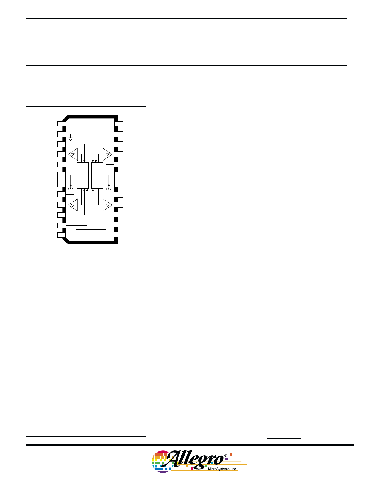
CONNECTION
LOGIC
GROUND
OUT
LOAD
SUPPLY
GROUND
GROUND
SENSE
OUT
PWM
NO
S
S
CP1
1
NC
2
10
3
4
1A
5
1
V
BB1
6
7
1
8
9
1B
9
10
11
11
1
12
LOGIC
CHARGE PUMP
LOGIC
24
DD
V
23
22
21
20
V
BB2
19
18
17
16
15
14
13
LOGIC
SUPPLY
2
PWM
S
20
OUT
2A
LOAD
SUPPLY
GROUND
GROUND
SENSE
OUT
2B
S
21
V
CP
CP2
Dwg. PP-069-2
DUAL DMOS
FULL-BRIDGE DRIVER
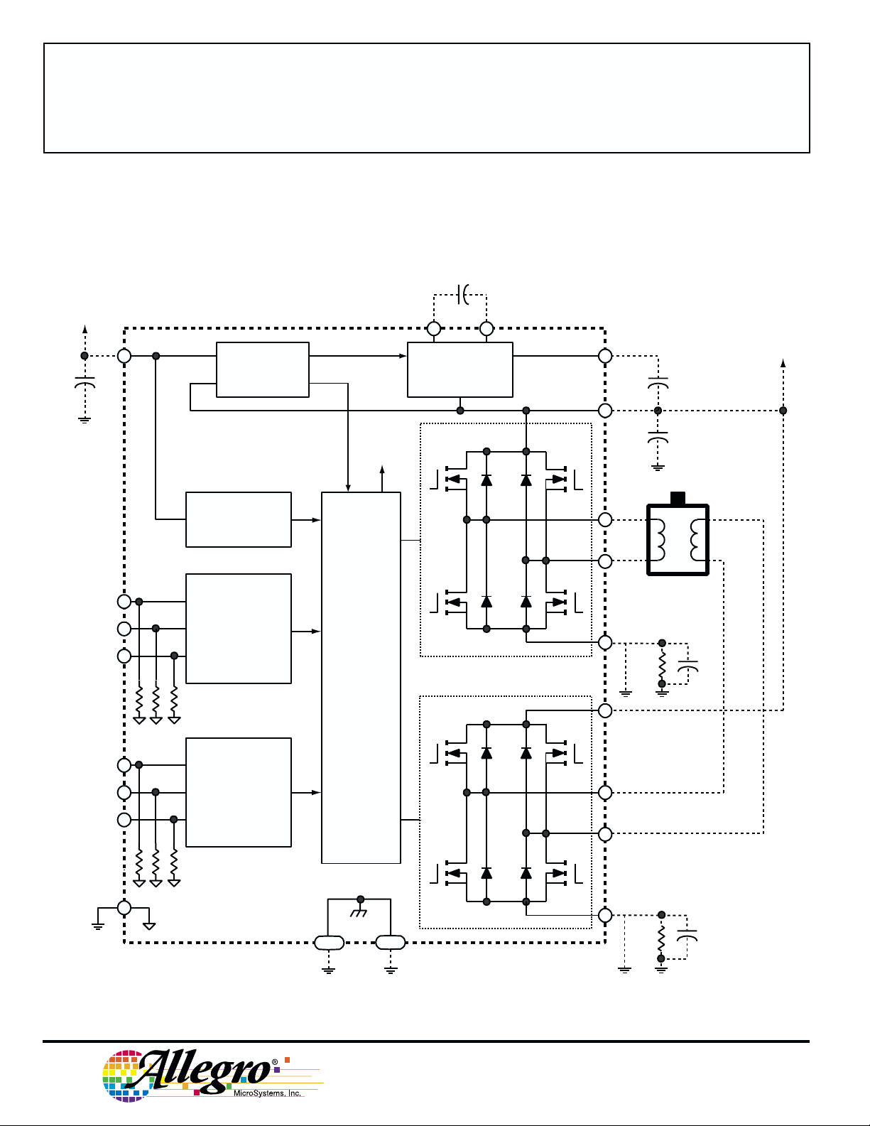
Designed to interface between external PWM control logic and
inductive loads such as relays, solenoids, dc motors, or stepper motors,
each full bridge can operate with output currents to ±2.5 A and operating
voltages to 50 V.
Low r
during PWM operation. Internal charge pump circuitry is used to create
a boosted voltage to fully enhance the high-side DMOS switches.
2
Three TTL-compatible logic-input terminals per bridge allow flexibility in configuring PWM control.
2
Internal circuit protection includes thermal shutdown with hysteresis,
and crossover-current protection. Special power -up sequencing is not
required.
The A3971SLB is supplied in a 24-lead plastic SOIC with a copper
batwing tab. The power tab is at ground potential and needs no electrical isolation.
DMOS output drivers provide low power dissipation
DS(on)
ABSOLUTE MAXIMUM RATINGS
at TA = +25°C
Load Supply Voltage, VBB................ 50 V
Output Current, I
Transient (<500 ns) ................... ±5 A
Logic Supply Voltage,
VDD............................................ 7.0 V
Sense Voltage, V
Logic Input Voltage Range,
VIN.................. -0.3 V to V
High-Side Gate Voltage ........... V
Package Power Dissipation,
PD............................................. 2.2 W
Operating Temperature Range,
TA............................. -20°C to +85°C
Junction Temperature, TJ............. +150°C
Storage Temperature Range,
TS........................... -55°C to +150°C
Output duty cycle, ambient temperature, and
heat sinking may limit current rating. Under
any set of conditions, do not exceed the
specified current rating or a junction temperature of 150 °C.
OUT
...................... 0.5 V
SENSE
DD
BB
+ 0.3 V
+ 8 V
FEATURES
■ ±2.5 A Load Current Capability per Bridge
■ Parallel Outputs for 5 A Load-Current Capability
■ Low r
Typically 325 mΩ source, 175 mΩ sink
■ Synchronous Rectification via Control Logic
■ Internal Undervoltage Monitor
■ Crossover-Current Protection
■ Source Connections for External Current Sensing
■ Thermal Shutdown Circuitry
Always order by complete part number: A3971SLB .
DS(on)
Outputs
3971
DUAL DMOS
FULL-BRIDGE DRIVER
LOGIC
SUPPLY
V
DD
24
VOLTAGE
REFERENCE
FUNCTIONAL BLOCK DIAGRAM
0.22 µF/100 V
CP1CP2
12
V
REF
LOW SIDE SUPPLY
V
CP
13
CHARGE PUMP
DMOS H-BRIDGE
V
CP
14
V
BB2
20
0.22 µF
50 V
LOAD
SUPPLY
S
S
PWM
PWM
LGND
UVLO &
THERMAL
OUT
2A
21
SHUTDOWN
OUT
2B
16
3
10
10
11
11
1
BRIDGE 1
CONTROL
LOGIC
GATE
17
SENSE
(OPTIONAL)
2
RS, C
S
DRIVE
DMOS H-BRIDGE
22
S
20
15
S
21
23
2
2
BRIDGE 2
CONTROL
LOGIC
5
V
OUT
4
OUT
9
SENSE
8
BB1
1A
1B
(OPTIONAL)
1
R
,
C
S
S
GROUND
6
7
18
19
115 Northeast Cutoff, Box 15036
Worcester, Massachusetts 01615-0036 (508) 853-5000
Copyright © 2000, Allegro MicroSystems, Inc.
Dwg. FP-050
3971
DUAL DMOS
FULL-BRIDGE DRIVER
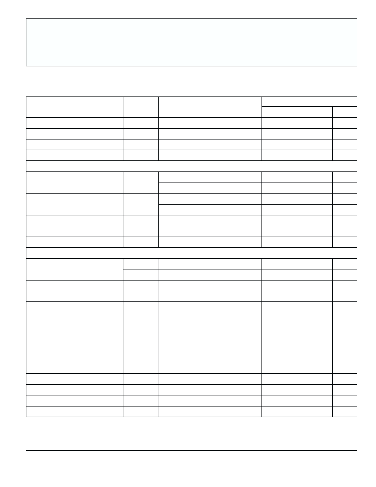
ELECTRICAL CHARACTERISTICS at TA = +25°C, VBB = 50 V, VDD = 5.0 V (unless otherwise noted).
Limits
Characteristic Symbol Test Conditions Min. Typ. Max. Units
Load Supply Voltage Range V
Logic Supply Voltage Range V
Load Supply Current I
Logic Supply Current I
Output Drivers
Output Leakage Current I
Output ON Resistance r
DS(on)
Body Diode Forward Voltage V
High-Side Gate Voltage V
Control Logic
Logic Input Voltage V
V
Logic Input Current I
I
Propagation Delay Time t
BB
DD
BB
DD
DSS
F
CP
IN(0)
IN(1)
IN(0)
IN(1)
PD
Operating 10 — 50 V
Operating 4.5 5.0 5.5 V
Operating, each supply, no load — — 3.0 mA
Operating — — 5.0 mA
V
= V
OUT
V
OUT
High-side switch, I
Low-side switch, I
BB
= 0 V — <-1.0 -20 mA
= -2.5 A — 325 375 mΩ
OUT
= 2.5 A — 175 200 mΩ
OUT
— <1.0 20 µA
Source diode, IF = 2.5 A — 1.2 — V
Sink diode, IF = 2.5 A — 1.0 — V
C = 0.22 µF, reference V
BB
6.0 6.5 7.0 V
——0.8V
2.0 — — V
VIN = 0 V — <1.0 -5.0 µA
VIN = 5.0 V — 20 50 µA
50% to 90%:
PWM change to source off — 50 — ns
PWM change to sink off — 60 — ns
PWM change to source on — 565 — ns
PWM change to sink on — 665 — ns
Disable to source on — 150 — ns
Disable to sink on — 250 — ns
Thermal Shutdown Temperature T
Thermal Shutdown Hysteresis ∆T
UVLO Threshold V
UVLO Hysteresis ∆V
J
J
UVLO
UVLO
Increasing V
NOTES: 1. Typical Data is for design information only.
2. Negative current is defined as coming out of (sourcing) the specified device terminal.
www.allegromicro.com
DD
— 165 — °C
—15—°C
3.9 4.15 4.4 V
—0.15— V
 Loading...