

Allegro A3968SLB, A3968SA Datasheet
3968
Data Sheet
29319.29
ADVANCE INFORMATION
(subject to change without notice)
September 3, 1999
A3968SLB
OUT
INPUT
INPUT
GROUND
SENSE
OUT
SUPPLY
REFERENCE
1
1A
V
2
1A
3
1B
4
5
1
6
1B
LOAD
710
89
REF
BB
LOGICLOGIC
V
BB
ABSOLUTE MAXIMUM RATINGS
Load Supply Voltage, VBB................... 30 V
Output Current, I
(continuous) .............................. ±650 mA
Logic Supply Voltage, VCC................. 7.0 V
Input Voltage, Vin..... -0.3 V to VCC + 0.3 V
Sense Voltage, VS................................ 1.0 V
Package Power Dissipation
A3968SA ................................... 2.08 W*
A3968SLB ................................. 1.87 W*
Operating Temperature Range,
TA................................... -20°C to +85°C
Junction Temperature,
TJ................................................. +150°C
Storage Temperature Range,
TS................................. -55°C to +150°C
Output current rating may be limited by duty
cycle, ambient temperature, and heat sinking.
Under any set of conditions, do not exceed the
specified current rating or a junction temperature
of 150°C.
* Per SEMI G42-88 Specification, Thermal Test
Board Standardization for Measuring Junctionto-Ambient Thermal Resistance of Semiconductor
Packages.
(peak) .......... ±750 mA
OUT
16
15
14
13
12
11
V
CC
RC
Dwg. PP-066
(TA = 25°C)
OUT
INPUT
INPUT
GROUND
SENSE
OUT
LOGIC
SUPPLY
RCV
, P
DUAL FULL-BRIDGE PWM
MOTOR DRIVER WITH BRAKE
The A3968SA and A3968SLB are designed to bidirectionally control two
dc motors. Each device includes two H-bridges capable of continuous output
currents of ±650 mA and operating voltages to 30 V. Motor winding current
can be controlled by the internal fixed-frequency, pulse-width modulated
2A
2A
2B
2
2B
D
(PWM), current-control circuitry. The peak load current limit is set by the
user’s selection of a reference voltage and current-sensing resistors. Except
for package style and pinout, the two devices are identical.
The fixed-frequency pulse duration is set by a user-selected external
RC timing network. The capacitor in the RC timing network also determines
a user-selectable blanking window that prevents false triggering of the PWM
current-control circuitry during switching transitions.
To reduce on-chip power dissipation, the H-bridge power outputs have
been optimized for low saturation voltages. The sink drivers feature Allegro’s
patented Satlington™ output structure. The Satlington outputs combine the
low voltage drop of a saturated transistor and the high peak current capability
of a Darlington.
For each bridge, the INPUT
and INPUTB terminals determine the load
A
current polarity by enabling the appropriate source and sink driver pair.
When a logic low is applied to both INPUTs of a bridge, the braking function
is enabled. In brake mode, both source drivers are turned OFF and both sink
drivers are turned ON, thereby dynamically braking the motor. When a logic
high is applied to both INPUTs of a bridge, all output drivers are disabled.
Special power-up sequencing is not required. Internal circuit protection
includes thermal shutdown with hysteresis, ground-clamp and flyback diodes,
and crossover-current protection.
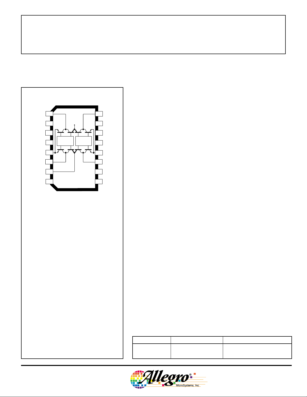
The A3968SA is supplied in a 16-pin dual in-line plastic package. The
A3968SLB is supplied in a 16-lead plastic SOIC with copper heat sink tabs.
The power tab is at ground potential and needs no electrical isolation.
FEATURES
■ ±650 mA Continuous Output Current
■ 30 V Output Voltage Rating
■ Internal Fixed-Frequency PWM Current Control
■ Satlington™ Sink Drivers
■ Brake Mode
■ User-Selectable Blanking Window
■ Internal Ground-Clamp & Flyback Diodes
■ Internal Thermal-Shutdown Circuitry
■ Crossover-Current Protection and UVLO Protection
Always order by complete part number:
Part Number Package R
θJA
A3968SA 16-pin DIP 60°C/W 38°C/W —
A3968SLB 16-lead batwing SOIC 67°C/W — 6°C/W
R
θJC
R
θJT
3968
DUAL FULL-BRIDGE
PWM MOTOR DRIVER
WITH BRAKE
FUNCTIONAL BLOCK DIAGRAM
(one-half of circuit shown)
INPUT
UVLO
& TSD
INPUT
GROUND
A
LOGIC
SUPPLY
V
A
CC
OUT
V
BB
B
OUT
LOAD
SUPPLY
+
CONTROL LOGIC
B
R
T
SOURCE
ENABLE
RC
PWM LATCH
Q
C
T
OSC
BLANKING
GATE
R
S
CURRENT-SENSE
COMPARATOR
TO OTHER
BRIDGE
TO OTHER
BRIDGE
SENSE
+
–
TO OTHER
BRIDGE
÷4
REFERENCE
R
S
Dwg. FP-036-4
SENSE
OUT
LOAD
SUPPLY
REFERENCE
RC
LOGIC
SUPPLY
OUT
SENSE
A3968SA
TRUTH TABLE
INPUT
1
1
2
1B
3
V
4
REF
RC
5
V
6
CC
7
2B
8
2
V
LOGIC
BB
LOGIC
16
15
14
13
12
11
10
9
Dwg. PP-066-3
INPUT
OUT
1B
1A
1A
INPUTAINPUT
OUT
B
LLLLBrake mode
L H L H “Forward”
H L H L “Reverse”
H H Z Z Disable
GROUND
GROUND
OUT
2A
INPUT
2A
INPUT
2B
115 Northeast Cutoff, Box 15036
Worcester, Massachusetts 01615-0036 (508) 853-5000
Copyright © 1998, Allegro MicroSystems, Inc.
Z = High impedance
OUT
A
B
Description
3968
DUAL FULL-BRIDGE
PWM MOTOR DRIVER
WITH BRAKE
ELECTRICAL CHARACTERISTICS at T
V
= 0 V, 56 kΩ & 680 pF RC to Ground (unless noted otherwise)
S
= +25°C, V
A
= 30 V, VCC = 4.75 V to 5.5 V, V
BB
REF
= 2 V,
Limits
Characteristic Symbol Test Conditions Min. Typ. Max. Units
Output Drivers
Load Supply Voltage Range V
Output Leakage Current I
Output Saturation Voltage V
CE(SAT)
Clamp Diode Forward Voltage V
Motor Supply Current I
(No Load)
BB(ON)
I
BB(OFF)
BB
CEX
F
Operating, I
V
= 30 V — <1.0 50 µA
OUT
V
= 0 V — <-1.0 -50 µA
OUT
Source Driver, I
Source Driver, I
Sink Driver, I
Sink Driver, I
= ±650 mA, L = 3 mH V
OUT
= -400 mA — 1.7 2.0 V
OUT
= -650 mA — 1.8 2.1 V
OUT
= +400 mA, VS = 0.5 V — 0.3 0.5 V
OUT
= +650 mA, VS = 0.5 V — 0.4 1.3 V
OUT
CC
—30 V
IF = 400 mA — 1.1 1.4 V
IF = 650 mA — 1.4 1.6 V
Both bridges ON (forward or reverse) — 3.0 5.0 mA
All INPUTs = 2.4 V — <1.0 200 µA
Control Logic
Logic Supply Voltage Range V
Logic Input Voltage V
V
Logic Input Current I
Reference Input Volt. Range V
Reference Input Current I
Reference Divider Ratio V
REF/VTRIP
Current-Sense Comparator V
IN(1)
I
IN(0)
REF
CC
IN(1)
IN(0)
REF
IO
Operating 4.75 — 5.50 V
V
IN
V
IN
Operating 0.1 – 2.0 V
V
REF
Input Offset Voltage
Current-Sense Comparator V
S
Operating -0.3 — 1.0 V
Input Voltage Range
Sense-Current Offset I
SO
IS – I
NOTES: 1. Typical Data is for design information only.
2. Negative current is defined as coming out of (sourcing) the specified device terminal.
2.4 — — V
— — 0.8 V
= 2.4 V — <1.0 20 µA
= 0.8 V — <-20 -200 µA
-2.5 0 1.0 µA
3.8 4.0 4.2 —
= 0.1 V -6.0 0 6.0 mV
, 50 mA ≤ I
OUT
≤ 650 mA 12 18 24 mA
OUT

3968
DUAL FULL-BRIDGE
PWM MOTOR DRIVER
WITH BRAKE
ELECTRICAL CHARACTERISTICS at T
V
= 0 V, 56 kΩ & 680 pF RC to Ground (unless noted otherwise) (cont.)
S
= +25°C, V
A
= 30 V, VCC = 4.75 V to 5.5 V, V
BB
REF
= 2 V,
Limits
Characteristic Symbol Test Conditions Min. Typ. Max. Units
Control Logic (continued)
PWM RC Frequency f
PWM Propagation Delay Time t
Cross-Over Dead Time t
Propagation Delay Times t
Thermal Shutdown Temp. T
Thermal Shutdown Hysteresis ∆T
UVLO Enable Threshold V
UVLO Hysteresis V
Logic Supply Current I
osc
PWM
codt
T(UVLO)+
T(UVLO)hys
CC(ON)
I
CC(OFF)
I
CC(BRAKE)
pd
J
J
CT = 680 pF, R
Comparator Trip to Source OFF — 1.0 1.4 µs
Cycle Reset to Source ON — 0.8 1.2 µs
1 kΩ Load to 25 V 0.2 1.8 3.0 µs
I
= ±650 mA, 50% to 90%:
OUT
Disable OFF to Source ON — 100 — ns
Disable ON to Source OFF — 500 — ns
Disable OFF to Sink ON — 200 — ns
Disable ON to Sink OFF — 200 — ns
Brake Enable to Sink ON — 2200 — ns
Brake Enable to Source OFF — 200 — ns
Increasing V
Both bridges ON (forward or reverse) — — 50 mA
All INPUTs = 2.4 V — — 9.0 mA
All INPUTs = 0.8 V — — 95 mA
= 56 kΩ 22.9 25.4 27.9 kHz
T
— 165 — °C
—15—°C
CC
— 4.1 4.6 V
0.1 0.6 — V
NOTES: 1. Typical Data is for design information only.
2. Negative current is defined as coming out of (sourcing) the specified device terminal.
115 Northeast Cutoff, Box 15036
Worcester, Massachusetts 01615-0036 (508) 853-5000
 Loading...