

Allegro A3966SA, A3966SLB Datasheet
A3966SLB
OUT
PHASE
ENABLE
GROUND
SENSE
OUT
LOAD
SUPPLY
REFERENCE
1
1A
V
2
1
3
1
4
5
1
6
1B
710
V
89
REF
BB
LOGICLOGIC
V
BB
16
OUT
PHASE
15
ENABLE
14
GROUND
13
12
SENSE
OUT
11
V
CC
RC
LOGIC
SUPPLY
RC
Dwg. PP-066-1
ABSOLUTE MAXIMUM RATINGS
Load Supply Voltage, VBB...................... 30 V
Output Current, I
(continuous) ..............................
Logic Supply Voltage, V
Input Voltage, V
Sense Voltage, V
Package Power Dissipation (T
A3966SA ..................................... 2.08 W*
A3966SLB ................................... 1.87 W*
Operating Temperature Range,
T
..................................... -20°C to +85°C
A
Junction Temperature,
T
.................................................. +150°C
J
Storage Temperature Range,
T
................................... -55°C to +150°C
S
Output current rating may be limited by duty cycle,
ambient temperature, and heat sinking. Under any set
of conditions, do not exceed the specified current rating
or a junction temperature of 150°C.
* Per SEMI G42-88 Specification, Thermal Test Board
Standardization for Measuring Junction-to-Ambient
Thermal Resistance of Semiconductor Packages.
(peak) ........... ±750 mA
OUT
±650 mA
.................... 7.0 V
CC
........ -0.3 V to VCC + 0.3 V
in
................................ 1.0 V
S
= 25°C), P
A
29319.25A†
Data Sheet
3966
DUAL FULL-BRIDGE PWM
MOTOR DRIVER
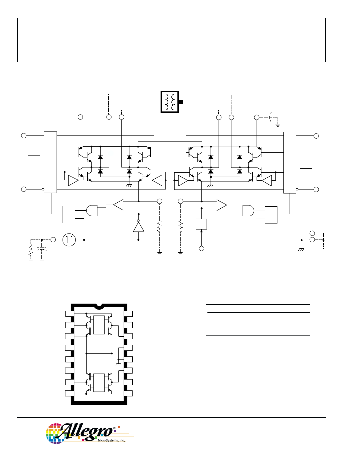
The A3966SA and A3966SLB are designed to drive both windings of a
two-phase bipolar stepper motor. Each device includes two H-bridges
capable of continuous output currents of ±650 mA and operating voltages to
30 V. Motor winding current can be controlled by the internal fixed-fre-
2A
2
2
2B
D
quency, pulse-width modulated (PWM), current-control circuitry. The peak
load current limit is set by the user’s selection of a reference voltage and
current-sensing resistors. Except for package style and pinout, the two
devices are identical.
2
The fixed-frequency pulse duration is set by a user-selected external
RC timing network. The capacitor in the RC timing network also determines
a user-selectable blanking window that prevents false triggering of the PWM
current-control circuitry during switching transitions.
To reduce on-chip power dissipation, the H-bridge power outputs have
been optimized for low saturation voltages. The sink drivers feature Allegro’s
patented Satlington™ output structure. The Satlington outputs combine the
low voltage drop of a saturated transistor and the high peak current capability
of a Darlington.
For each bridge, a PHASE input controls load-current polarity by
selecting the appropriate source and sink driver pair. For each bridge, an
ENABLE input, when held high, disables the output drivers. Special powerup sequencing is not required. Internal circuit protection includes thermal
shutdown with hysteresis, ground-clamp and flyback diodes, and crossovercurrent protection.
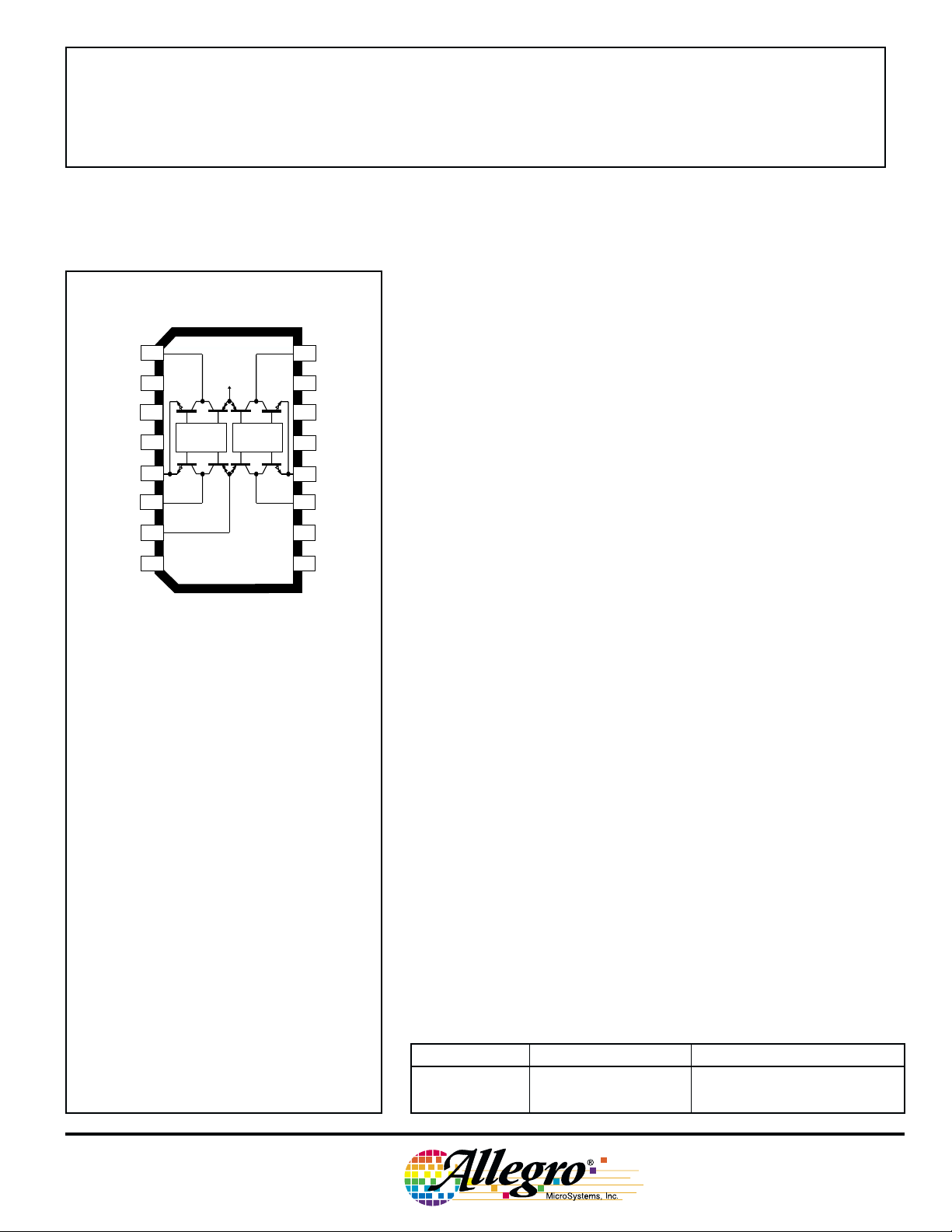
The A3966SA is supplied in a 16-pin dual in-line plastic package. The
A3966SLB is supplied in a 16-lead plastic SOIC with copper heat sink tabs.
The power tab is at ground potential and needs no electrical isolation.
FEATURES
■ ±650 mA Continuous Output Current
■ 30 V Output Voltage Rating
■ Internal Fixed-Frequency PWM Current Control
■ Satlington™ Sink Drivers
■ User-Selectable Blanking Window
■ Internal Ground-Clamp & Flyback Diodes
■ Internal Thermal-Shutdown Circuitry
■ Crossover-Current Protection and UVLO Protection
Always order by complete part number:
Part Number Package R
θJA
A3966SA 16-pin DIP 60°C/W 38°C/W —
A3966SLB 16-lead batwing SOIC 67°C/W — 6°C/W
R
θJC
R
θJT
3966
DUAL FULL-BRIDGE
PWM MOTOR DRIVER
LOGIC
SUPPLY
V
CC
PHASE
1
1
FUNCTIONAL BLOCK DIAGRAM
1A
1B
OUT
OUT
V
BB
2A
OUT
2B
OUT
LOAD
SUPPLY
+
PHASE
2
2
ENABLE
R
T
UVLO
& TSD
1
CONTROL LOGIC
1
SOURCE
ENABLE
RC
C
T
SENSE
OUT
LOAD
SUPPLY
REFERENCE
RC
LOGIC
SUPPLY
OUT
SENSE
PWM LATCH
Q
S
OSC
1
1
2
1B
3
4
5
6
7
2B
8
2
1
R
V
REF
RC
V
CC
CURRENT-SENSE
BLANKING
GATE
COMPARATOR
1
A3966SA
LOGIC
V
BB
LOGIC
UVLO
& TSD
CONTROL LOGIC
ENABLE
2
÷4
REFERENCE
CURRENT-SENSE
COMPARATOR
+
–
2
BLANKING
GATE
2
PWM LATCH
R
S
2
2
SOURCE
ENABLE
Q
GROUND
Dwg. FP-036-6
1
+
–
SENSE
R
1S
SENSE
1
2
R
2S
TRUTH TABLE
16
15
14
13
12
11
10
9
ENABLE
PHASE
OUT
1A
GROUND
GROUND
OUT
2A
PHASE
ENABLE
PHASE ENABLE OUT
1
1
XH OffOff
HL H L
LL L H
X = Irrelevant
2
2
OUT
A
B
Dwg. PP-066-2
2
115 Northeast Cutoff, Box 15036
Worcester, Massachusetts 01615-0036 (508) 853-5000
Copyright © 1998, 2000 Allegro MicroSystems, Inc.

3966
DUAL FULL-BRIDGE
PWM MOTOR DRIVER
ELECTRICAL CHARACTERISTICS at TA = +25°C, VBB = 30 V, VCC = 4.75 V to 5.5 V, V
REF
= 2 V,
VS = 0 V, 56 kΩ & 680 pF RC to Ground (unless noted otherwise)
Limits
Characteristic Symbol Test Conditions Min. Typ. Max. Units
Output Drivers
Load Supply Voltage Range V
Output Leakage Current I
Output Saturation Voltage V
Clamp Diode Forward Voltage V
Motor Supply Current I
(No Load)
Control Logic
BB
CEX
CE(SAT)
F
BB(ON)
I
BB(OFF)
Operating, I
V
= 30 V — <1.0 50 µA
OUT
V
= 0 V — <-1.0 -50 µA
OUT
Source Driver, I
Source Driver, I
Sink Driver, I
Sink Driver, I
= ±650 mA, L = 3 mH V
OUT
= -400 mA — 1.7 2.0 V
OUT
= -650 mA — 1.8 2.1 V
OUT
= +400 mA, VS = 0.5 V — 0.3 0.5 V
OUT
= +650 mA, VS = 0.5 V — 0.4 1.3 V
OUT
CC
—30 V
IF = 400 mA — 1.1 1.4 V
IF = 650 mA — 1.4 1.6 V
V
V
ENABLE1
ENABLE1
= V
= V
= 0.8 V — 3.0 5.0 mA
ENABLE2
= 2.4 V — <1.0 200 µA
ENABLE2
Logic Supply Voltage Range V
Logic Input Voltage V
V
Logic Input Current I
I
Reference Input Volt. Range V
Reference Input Current I
Reference Divider Ratio V
REF/VTRIP
Current-Sense Comparator V
CC
IN(1)
IN(0)
IN(1)
IN(0)
REF
REF
IO
Operating 4.75 — 5.50 V
V
IN
V
IN
Operating 0.1 – 2.0 V
V
REF
Input Offset Voltage
Current-Sense Comparator V
S
Operating -0.3 — 1.0 V
Input Voltage Range
Sense-Current Offset I
SO
IS – I
NOTES:1. Typical Data is for design information only.
2. Negative current is defined as coming out of (sourcing) the specified device terminal.
2.4 — — V
— — 0.8 V
= 2.4 V — <1.0 20 µA
= 0.8 V — <-20 -200 µA
-2.5 0 1.0 µA
3.8 4.0 4.2 —
= 0 V -6.0 0 6.0 mV
, 50 mA ≤ I
OUT
≤ 650 mA 12 18 24 mA
OUT
www.allegromicro.com
3
3966
DUAL FULL-BRIDGE
PWM MOTOR DRIVER
ELECTRICAL CHARACTERISTICS at TA = +25°C, VBB = 30 V, VCC = 4.75 V to 5.5 V, V
REF
= 2 V,
VS = 0 V, 56 kΩ & 680 pF RC to Ground (unless noted otherwise) (cont.)
Limits
Characteristic Symbol Test Conditions Min. Typ. Max. Units
Control Logic (continued)
PWM RC Frequency f
PWM Propagation Delay Time t
Cross-Over Dead Time t
PWM
codt
Propagation Delay Times t
Thermal Shutdown Temp. T
Thermal Shutdown Hysteresis ∆T
UVLO Enable Threshold V
UVLO Hysteresis V
Logic Supply Current I
T(UVLO)+
T(UVLO)hys
CC(ON)
I
CC(OFF)
osc
pd
J
J
CT = 680 pF, RT = 56 kΩ 22.9 25.4 27.9 kHz
Comparator Trip to Source OFF — 1.0 1.4 µs
Cycle Reset to Source ON — 0.8 1.2 µs
1 kΩ Load to 25 V 0.2 1.8 3.0 µs
I
= ±650 mA, 50% to 90%:
OUT
ENABLE ON to Source ON — 100 — ns
ENABLE OFF to Source OFF — 500 — ns
ENABLE ON to Sink ON — 200 — ns
ENABLE OFF to Sink OFF — 200 — ns
PHASE Change to Sink ON — 2200 — ns
PHASE Change to Sink OFF — 200 — ns
PHASE Change to Source ON — 2200 — ns
PHASE Change to Source OFF — 200 — ns
— 165 — °C
—15—°C
Increasing V
CC
— 4.1 4.6 V
0.1 0.6 — V
V
ENABLE 1
V
ENABLE 1
= V
= V
ENABLE 2
ENABLE 2
= 0.8 V — — 50 mA
= 2.4 V — — 9.0 mA
NOTES:1. Typical Data is for design information only.
2. Negative current is defined as coming out of (sourcing) the specified device terminal.
4
115 Northeast Cutoff, Box 15036
Worcester, Massachusetts 01615-0036 (508) 853-5000
 Loading...