


查询A3965供应商查询A3965供应商
These parts are in production but have been determined to be
NOT FOR NEW DESIGN. This classification indicates that sale of
this device is currently restricted to existing customer applications.
The device should not be purchased for new design applications
because obsolescence in the near future is probable. Samples are no
longer available.
A3965
DMOS Dual Full-Bridge PWM Motor Driver
Not for New Design
Date of status change: November 1, 2004
Recommended Substitutions:
The A3965 is a fairly unique device within Allegro’s portfolio, typically
fitting niche low-voltage, battery-driven stepper motor applications.
Our closest recommended alternatives are:
• For customers looking for a stepper motor driver for battery-driven
applications, we recommend the A3977, A3982, A3983, or A3984.
• The closest device functionally is the A3966, if supply current and a
low logic voltage (4.75 to 5.5 V) are not issues.
NOTE: For detailed information on purchasing options, contact your
local Allegro field applications engineer or sales representative.
Allegro MicroSystems, Inc. reserves the right to make, from time to time, revisions to the anticipated product life cycle plan for a
product to accommodate changes in production capabilities, alternative product availabilities, or market demand. The information
included herein is believed to be accurate and reliable. However, Allegro MicroSystems, Inc. assumes no responsibility for its use; nor
for any infringements of patents or other rights of third parties which may result from its use.

PRELIMINARY DATASHEET - 12/4/2002
D
E
(Subject to change without notice)
ABSOLUTE MAXIMUM RATINGS
at TA = +25°C
Load Supply Voltage, VBB ..........................20 V
Output Current, I
Logic Supply Voltage, VDD..........................7.0 V
Logic Input Voltage Range,
VIN......................-0.3 V to V
(tW<30ns) ..................-1.0V to VDD +1V
Sense Voltage, V
Reference Voltage, V
Package Power Dissipation (TA = +25°C), P
A3965SLB........................... 50°C/W**
............................ ±500 mA*
OUT
DD
..................................0.5 V
SENSE
.................................3 V
REF
+ 0.3 V
D
3965
MOS DUAL FULL-BRIDG
PWM MOTOR DRIVER
Designed for Pulse Width Modulated (PWM) current control of low
voltage stepper motors, the A3965S is capable of output currents to ± 500 mA
and operating voltages to 20 V.
The A3965 is particularly attractive for low power or battery
operated motors where minimal power consumption is desired. A SLEEP
mode disables all circuitry and typically draws less than 1µA supply current
from motor and logic supply. During operation the fixed frequency ON
pulses of each H-bridge are 180 degrees out of phase to minimize the peak
demand required of the motor supply allowing savings in size and cost of
external power supply components.
PHASE and ENABLE input terminals are provided for use in
controlling the speed and direction of a stepper motor with externally applied
PWM control signals.
Operating Temperature Range,
TA................................ -20°C to +85°C
Junction Temperature, TJ......................... +150°C
Storage Temperature Range,
TS............................... -55°C to +150°C
* Output current rating may be limited by duty cycle,
ambient temperature, and heat sinking. Under any set of
conditions, do not exceed the specified current rating or a
junction temperature of 150°C.
*Measured with 062" thick FR4, two sided PCB with 1 sq
inch copper area.
Internal circuit protection includes thermal shutdown with
hysteresis, undervoltage monitoring of V
current protection. Special power up sequencing is not required.
The A3965 is supplied in a 24-lead plastic SOIC with a copper
batwing tab (suffix ‘LB’).
and charge pump, and crossover
DD
FEATURES
±500 mA, 20 V Output Rating
2.85 to 5.5V Logic Supply Operation
Sleep Mode for Minimum Power Consumption
Fixed Frequency PWM
Offset On Pulses to Minimize Peak Supply Transient Currents
Internal UVLO and Thermal Shutdown Circuitry
Crossover-Current Protection
1
3965 DMOS Dual Full Bridge
PWM Motor Driver
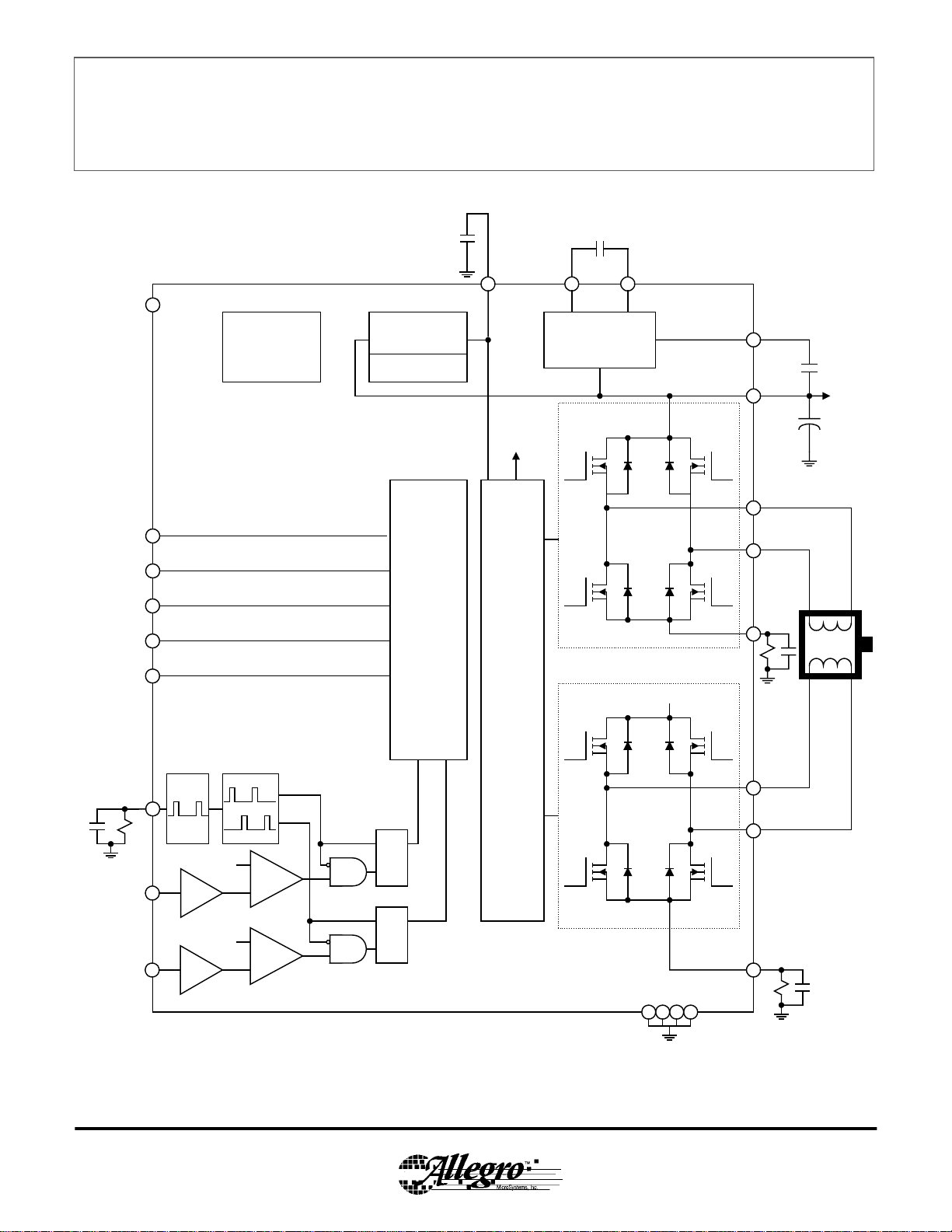
Functional Block Diagram
V
SLEEP
PHASE2
PHASE1
ENABLE1
ENABLE2
.22uf
VREG
DD
UVLO AND
REGULATOR
FAULT
DETECT
BANDGAP
.22uf
CP2
CHARGE PUMP
CP1
V
CP
V
BB
.22uf
DMOS H-BRIDGE
V
CP
OUT
1A
OUT
1B
CONTROL
SENSE1
LOGIC
GATE
DRIVE
DMOS H-BRIDGE
V
BB
OUT
2A
OUT
2B
SENSE2
.1uF
RC
REF2
REF1
OSC
SENSE2
1/6
SENSE1
1/6
+-
SRQ
SRQ
+-
GROUND
2

3965 DMOS Dual Full Bridge
PWM Motor Driver
ELECTRICAL CHARACTERISTICS at T
noted otherwise)
= +25°C, V
A
= 20 V, VDD = 3.0 V, V
BB
SENSE
= 0.5 V, f
< 50KHz (unless
PWM
Limits
Characteristics Symbol Test Conditions Min. Typ. Max. Units
Output Drivers
Load Supply Voltage Range VBB Operating, I
During Sleep Mode 0 20 V
Output Leakage Current I
Output On Resistance R
DSS
DSON
V
= V
OUT
V
= 0 V – <–1.0 -20 µA
OUT
Source Driver, I
Sink Driver, I
Source Driver, I
Sink Driver, I
Body Diode Forward Voltage V
F
Source Diode, IF = -500 mA – 1 – V
Sink Diode, IF = 500mA – 1 – V
Motor Supply Current I
BB
f
< 50 kHz – 3.5 7 mA
PWM
= ±500 mA 6 – 20 V
OUT
BB
= -500 mA – 1.2 1.35
OUT
= 500 mA – .75 .9
OUT
= -500 mA; VBB=6V 1.3 1.5
OUT
= 500 mA, VBB=6V .85 1.0
OUT
– <1.0 20 µA
Ω
Ω
Ω
Ω
Logic Supply Current
Control Logic
Logic Supply Voltage Range V
Logic Input Voltage V
Logic Input Current I
Charge Pump On, Outputs Disabled – 1.5 3 mA
Sleep Mode – – 10 uA
I
DD
f
< 50 kHz 4.5 mA
PWM
Outputs Off 3.6 mA
Sleep Mode (Inputs below .5V) <1 10 µA
DD
IN(1)
V
IN(0)
IN(1)
I
IN(0)
Operating 2.85 5.5 V
VDD*.7 – V
– VDD*.3 V
VIN = VDD*.7 -20 <1.0 20 µA
V
= VDD*.3 -20 <1.0 20 µA
IN
3

3965 DMOS Dual Full Bridge
PWM Motor Driver
ELECTRICAL CHARACTERISTICS at T
= +25°C, V
A
= 20V, VDD = 3.0 V, V
BB
= 0.5 V (unless noted otherwise)
SENSE
Limits
Characteristics Symbol Test Conditions Min. Typ. Max. Units
Control Logic
Reference Input Current I
VREF input voltage range V
Reference Divider Ratio V
(Note 3)
Propagation Delay t
REF
REF
REF/VS
ERR
PD
V
= V
REF
DD
V
= 1.5V -5 5 %GM Error V
REF
V
= .5V -10 10 %
REF
PWM CHANGE TO SOURCE OFF – 150 – ns
PWM CHANGE TO SINK OFF – 150 – ns
PWM CHANGE TO SOURCE ON – 1000 – ns
PWM CHANGE TO SINK ON – 1000 – ns
DISABLE TO SOURCE ON – 200 – ns
DISABLE TO SINK ON – 200 – ns
-1 0 1 µA
0 VDD- .1
6
t
COD
PWM RC Frequency f
Blank Time t
Thermal Shutdown Temp. T
Thermal Shutdown Hysteresis ∆T
UVLO Enable Threshold Rising V
UVLO Hysteresis 0.05 0.10 – V
OSC
BLANK
J
J
R = 1000pf, C = 20K 47.4 Khz
R = 1000pf, C = 20K .8 1.21 1.6 µs
DD
300 850 1200 ns
– 165 °C
– 15 – °C
2.5 2.8 V
NOTES: 1. Typical Data is for design information only.
2. Negative current is defined as coming out of (sourcing) the specified device pin.
3. V
ERR
=((V
REF
/6) – V
SENSE
)/(V
REF
/6)
4

3965 DMOS Dual Full Bridge
PWM Motor Driver
Functional Description
Sleep Mode. The input pin SLEEP is dedicated to put the
device into a minimum current draw mode. All circuits are
disabled including the VDD undervoltage monitor.
Shutdown. In the event of a fault due to excessive
junction temperature, or low voltage on V
CP
or V
outputs of the device are disabled until the fault condition is
removed. At power up, and in the event of low V
UVLO circuit disables the drivers
REG
DD
, the
, the
Current Regulation. Load current is regulated by a
fixed frequency PWM control circuit. When the outputs of
the DMOS H-bridge are turned on, current increases in the
motor winding until it reaches a value given by:
I
= V
TRIP
REF
/(6*R
At the trip point, the sense comparator resets the source
enable latch, turning off the source. At this point, load
inductance causes the current to recirculate until the end
fixed frequency cycle. (see timing diagram)
VREF. The V
voltage is divided down by 6 and
REF
compared to the voltage across the sense resistor to set the
value of bridge current that will trip the PWM comparator.
The V
connected to V
input is a high impedance input and can be
REF
, if desired, as well as via resistor divider.
DD
Note: When connected to V
greater than V
to allow proper headroom for the buffer
DD
output.
SENSE
DD
)
, the V
voltage must be 1.8V
BB
Fixed Frequency PWM. Selection of an external RC
sets the oscillator frequency as follows:
f
= 1/ ( 850ns + t
OSC
BLANK+RTCT
))
Blank Time. When a source driver turns on, a current
spike occurs due to the reverse recovery currents of the
clamp diodes and/or switching transients related to
distributed capacitance in the load. To prevent this current
spike from erroneously resetting the source enable latch, the
sense comparator is blanked. The blank duration is
determined by the time it takes to charge the external RC
.38*V
volts with a 1mA current source.
DD
t
= CT*.38*VDD/ ( 1mA – ( .41*VDD/RT))
BLANK
VREG. This supply voltage is used to run the sink side
DMOS outputs. VREG is internally monitored and in the
case of a fault condition, the outputs of the device are
disabled. The VREG pin should be decoupled with a 0.22
µF capacitor to ground.
Charge Pump. The Charge Pump is used to generate a
supply above VBB
0.22 uF ceramic monolithic capacitor should be connected
between CP
ceramic monolithic capacitor should be connected between
and VBB to act as a reservoir to run the high side
V
CP
DMOS devices. The V
in the case of a fault condition the outputs of the device are
disabled.
to drive the source side DMOS gates. A
and CP2 for pumping purposes. A 0.22 uF
1
Voltage is internally monitored and
CP
Thermal protection. Circuitry turns OFF all drivers
when the junction temperature reaches 165°C typically. It is
intended only to protect the device from failures due to
excessive junction temperatures and should not imply that
output short circuits are permitted. Thermal shutdown has a
hysteresis of approximately 15°C.
5

Control Logic
3965 DMOS Dual Full Bridge
PWM Motor Driver
Phase Enable Sleep Chopping
(Vs>V
REF
X X 0 X Off Off Sleep
X 1 1 X Off Off Fast Decay
0 0 1 0 L H Forward
0 0 1 1 L L Slow Decay Chop
1 0 1 0 H L Reverse
1 0 1 1 L L Slow Decay Chop
/6)
OUT
OUT
A
B
Function
Typical PWM Waveforms (Phase = 1)
RC
BLANK1
OUT1A
IOUT1
VSENSE1
BLANK2
OUT2A
IOUT2
VSENSE2
6

3965 DMOS Dual Full Bridge
PWM Motor Driver
Terminal List
Pin Name Pin Description SOIC 24
VREG Regulator decoupling Terminal 1
RC Analog Input for fixed frequency 2
SLEEP Logic input for SLEEP mode 3
VDD Logic Supply Voltage 4
OUT1B DMOS H – Bridge 1 Output B 5
GND Ground 6,7
SENSE1 Sense Resistor Terminal for Bridge 2 8
OUT1A DMOS H – Bridge 1 Output A 9
ENABLE1 Logic Input for Bridge 1 Enable Control 10
PHASE1 Logic Input for Bridge 1 PHASE Control 11
REF1 Gm Reference Input Voltage Bridge 2 12
REF2 Gm Reference Input Voltage Bridge 1 13
PHASE2 Logic Input for Bridge 2 PHASE Control 14
ENABLE2 Logic Input for Bridge 2 Enable Control 15
OUT2B DMOS H – Bridge 2 Output B 16
SENSE2 Sense Resistor Terminal for Bridge 1 17
GND Ground 18,19
OUT2A DMOS H – Bridge 2 Output A 20
VCP Reservoir Capacitor Terminal 21
CP2 Charge Pump Capacitor Terminal 22
CP1 Charge Pump Capacitor Terminal 23
VBB Load Supply 24
7
 Loading...