

Allegro A3964SLB, A3964SB Datasheet
3964
DUAL FULL-BRIDGE
PWM MOTOR DRIVER
DUAL FULL-BRIDGE PWM MOTOR DRIVER
3964
Data Sheet
29319.28*
A3964SLB
1
OUT
1B
1
OUT
LOAD
REF(IN)
RC
2
1
3
1A
4
5
6
7
9
8
1
9
1
10
1
V
BB
θ
1
PWM 1
SENSE
SUPPLY
GROUND
GROUND
V
PHASE
ENABLE
ABSOLUTE MAXIMUM RATINGS
Load Supply Voltage, VBB. . . . . . . . . 33 V
Output Current, I
(continuous). . . . . . . . . . . . .
Logic Supply Voltage, V
Logic Input Voltage Range,
V
. . . . . . . . . . . -0.3 V to VCC + 0.3 V
IN
Sense Voltage, V
Reference Output Current,
I
REF(OUT)
Package Power Dissipation,
P
. . . . . . . . . . . . . . . . . . . . See Graph
D
Operating Temperature Range,
T
. . . . . . . . . . . . . . . . -20˚C to +85˚C
A
Junction Temperature, T
Storage Temperature Range,
T
. . . . . . . . . . . . . . . -55˚C to +150˚C
S
* Output current rating may be limited by duty cycle,
ambient temperature, and heat sinking. Under any set
of conditions, do not exceed the specified current rating
or a junction temperature of 150˚C.
† Fault conditions that produce excessive junction
temperature will activate the device’s thermal shutdown
circuitry. These conditions can be tolerated but should
be avoided.
(10 µs) . . . . . . ±1.0 A*
OUT
CC
. . . . . . . . . . . . . . . 1.0 V
S
. . . . . . . . . . . . . . . . . . 1.0 mA
J
20
OUT
2B
2
19
SENSE
2
18
OUT
2A
LOGIC
17
V
CC
SUPPLY
16
GROUND
15
GROUND
V
14
REF(OUT)
13
RC
12
11
2
PHASE
ENABLE
Dwg. PP-047-1
2
2
PWM 2
θ
2
±800 mA*
. . . . . . . . . 7.0 V
. . . . . . . +150˚C†
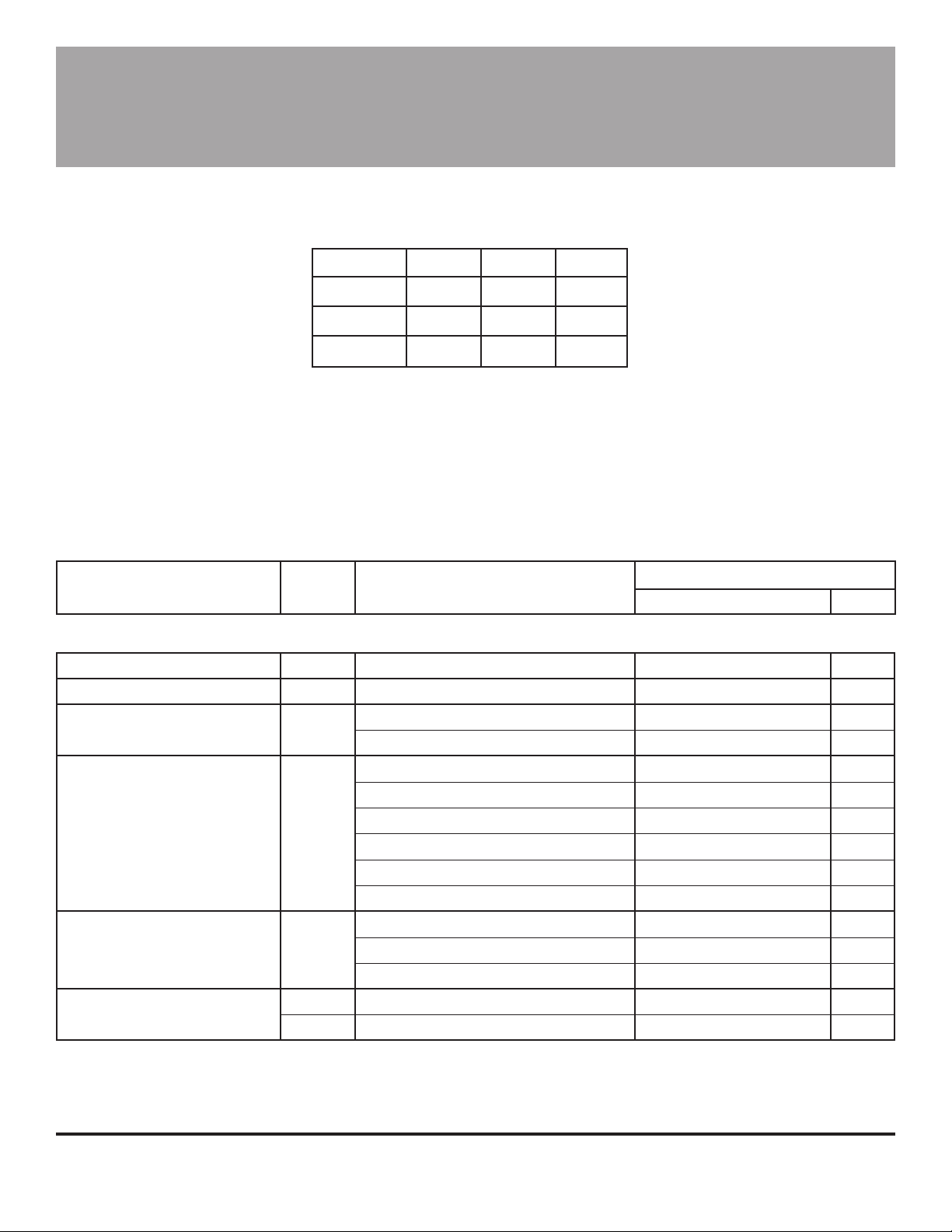
Designed for pulse-width modulated (PWM) current control of
bipolar stepper motors, the A3964SB and A3964SLB are capable of
continuous output currents to ±800 mA and operating voltages to 30 V.
Internal fixed off-time PWM current-control circuitry can be used to
regulate the maximum load current to a desired value. An internal
precision voltage reference is provided to improve motor peak-current
control accuracy. The peak load current limit is set by the user’s
selection of an external resistor divider and current-sensing resistors.
The fixed off-time pulse duration is set by user-selected external
RC timing networks. The capacitor in the RC timing network also
determines a user-selectable blanking window that prevents false
triggering of the PWM current control circuitry during switching transitions. This eliminates the need for two external RC filter networks on
the current-sensing comparator inputs.
For each bridge the PHASE input controls load current polarity by
selecting the appropriate source and sink driver pair. For each bridge
the ENABLE input, when held high, disables the output drivers. Special power-up sequencing is not required. Internal circuit protection
includes thermal shutdown with hysteresis, transient-suppression
diodes, and crossover-current protection.
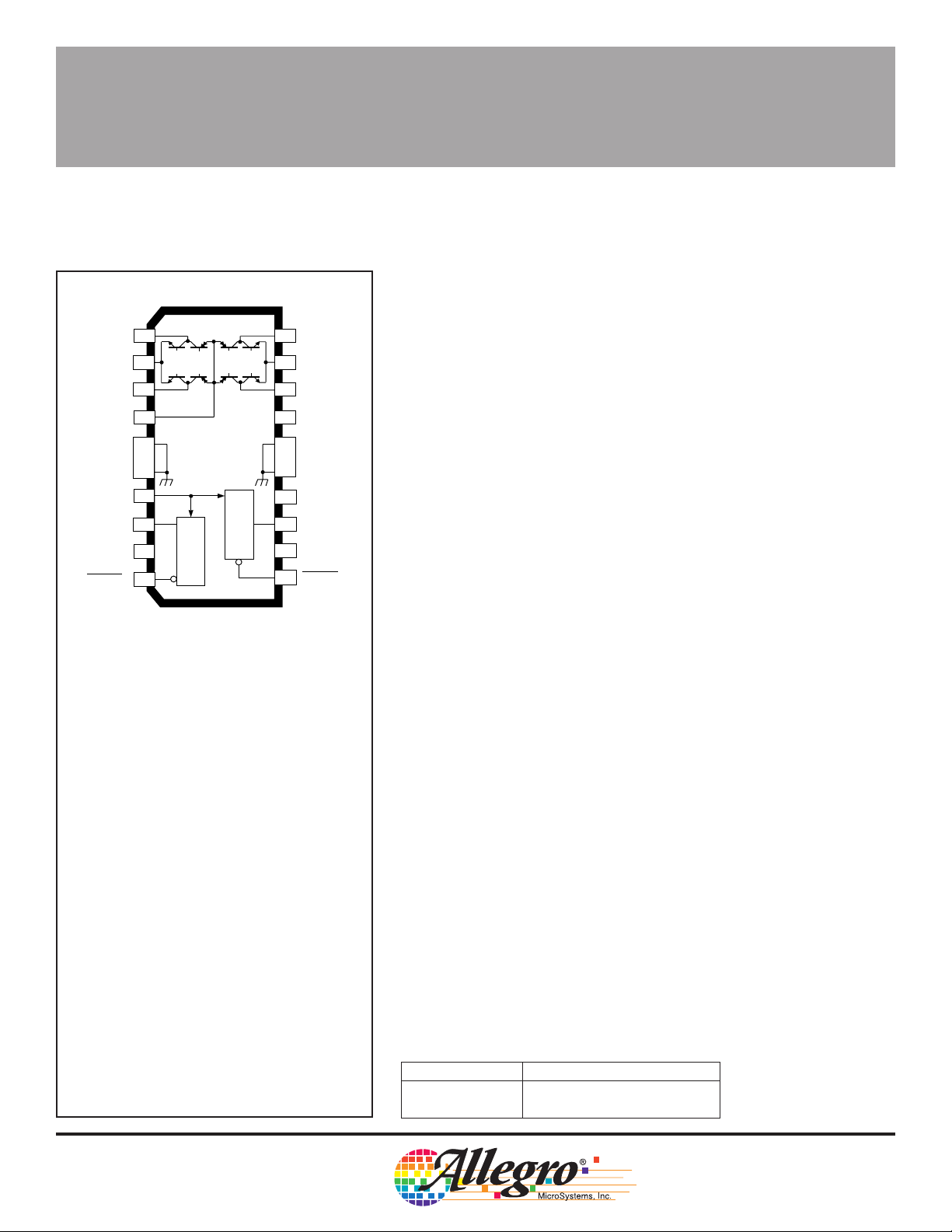
The A3964SB is supplied in a 24-pin plastic DIP with copper heat
sink tabs; A3964SLB is supplied in a 20-lead plastic SOIC with copper
heat sink tabs. The power tabs are at ground potential and need no
electrical isolation.
FEATURES
■ ±800 mA Continuous Output Current Rating
■ 30 V Output Voltage Rating
■ Internal PWM Current Control, Saturated Sink Drivers
■ Internally Generated, Precision 2.5 V Reference
■ Internal Transient-Suppression Diodes
■ Internal Thermal-Shutdown Circuitry
■ Crossover-Current Protection, UVLO Protection
Always order by complete part number:
Part Number Package
A3964SB 24-Pin DIP
A3964SLB 20-Lead Wide-Body SOIC
3964
1452
19
–
–
8109
3141820
7
121113
17
61516
DUAL FULL-BRIDGE
PWM MOTOR DRIVER
A3964SB
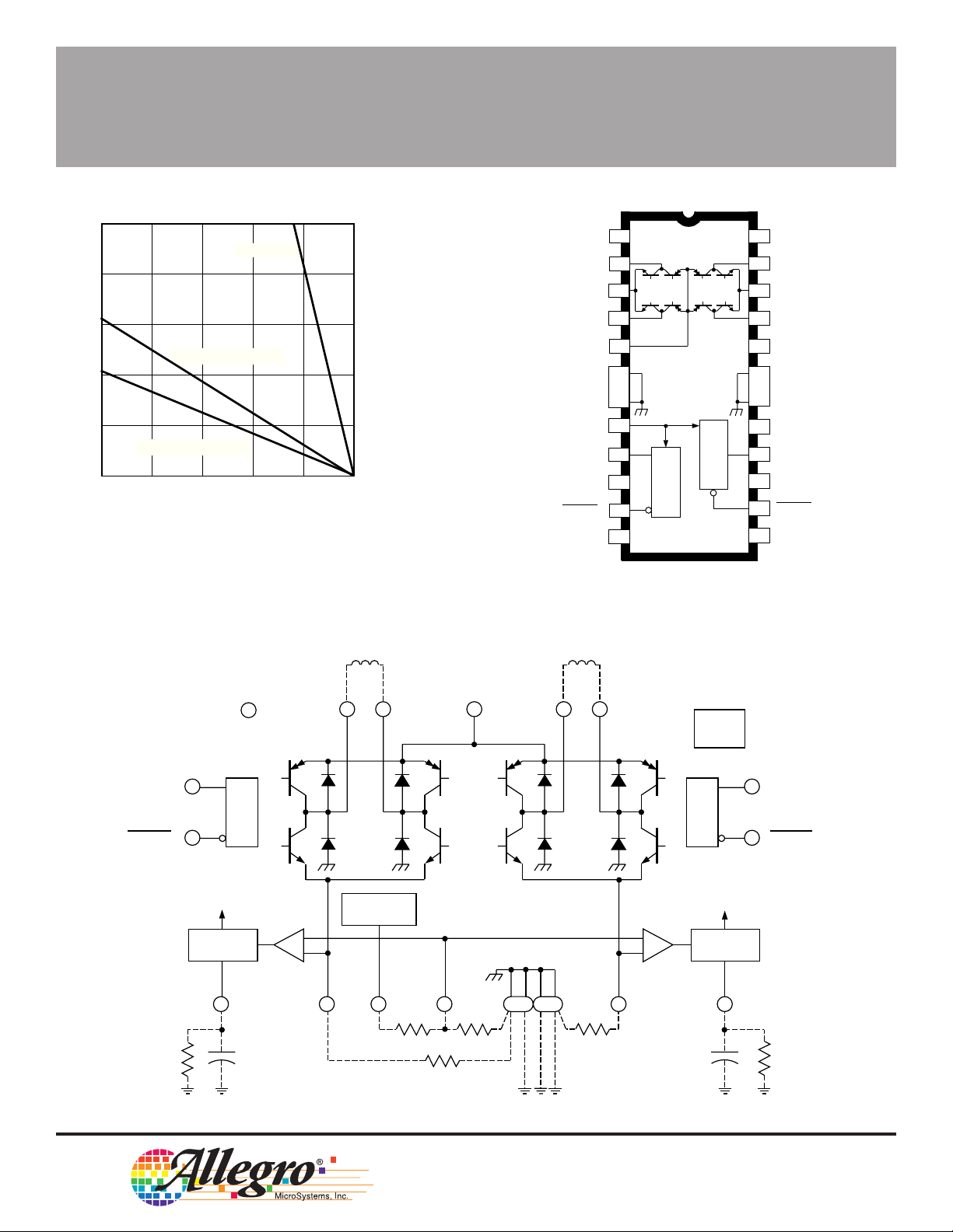
5
R = 6.0°C/W
θJT
4
3
SUFFIX 'B', R = 40°C/W
2
1
SUFFIX 'LB', R = 60°C/W
0
25
ALLOWABLE PACKAGE POWER DISSIPATION IN WATTS
50 75 100 125 150
TEMPERATURE IN °C
θJA
θJA
Dwg. GP-049-4
FUNCTIONAL BLOCK DIAGRAM
CONNECT.
OUT
SENSE
OUT
LOAD
SUPPLY
GROUND
GROUND
V
REF(IN)
PHASE
ENABLE
CONNECT.
(A3964SLB pinning shown)
RC
NO
NO
1
NC
2
1B
1
3
1
4
1A
5
6
7
8
9
9
1
10
θ
1
1
11
1
12
NC
V
BB
PWM 1
2
V
PWM 2
NC
NC
NO
24
CONNECT.
23
OUT
2B
22
SENSE
2
21
OUT
2A
LOGIC
20
CC
SUPPLY
19
GROUND
18
GROUND
17
V
REF(OUT)
16
RC
2
15
PHASE
θ
2
14
13
2
ENABLE
NO
CONNECT.
Dwg. PP-005-2
2
PHASE
ENABLE
1
1
R
T
SOURCE
DISABLE
ONE SHOT
1
RC
C
T
LOGIC
V
CC
PWM 1
SUPPLY
+
SENSE
OUT
1
1A
1
2.5 V
REFERENCE
OUT
REF
1B
OUT
R
A
IN
REF
R
S
V
V
REF(IN)
LOAD
BB
R
SUPPLY
B
2A
OUT
2B
OUT
UVLO
& TSD
PHASE
2
2
PWM 2
ENABLE
2
SOURCE
DISABLE
+
2
ONE SHOT
2
RC
R
SENSE
S
C
T
R
T
Dwg. FP-033-1
115 Northeast Cutoff, Box 15036
Worcester, Massachusetts 01615-0036 (508) 853-5000
Copyright © 1997 Allegro MicroSystems, Inc.
3964
DUAL FULL-BRIDGE
PWM MOTOR DRIVER
TRUTH TABLE
ENABLE PHASE OUT
OUT
A
B
H X Off Off
L HHL
LLLH
X = Irrelevant
ELECTRICAL CHARACTERISTICS at T
V
= 0 V, 30 kΩ & 1000 pF RC to Ground (unless noted otherwise)
S
Characteristic Symbol Test Conditions Min. Typ. Max. Units
= +25°C, V
A
= 30 V, VCC = 4.75 V to 5.25 V,
BB
Limits
Output Drivers
Load Supply Voltage Range V
Output Sustaining Voltage V
CE(sus)
Output Leakage Current I
Output Saturation Voltage V
CE(SAT)
Clamp Diode Forward Voltage V
(Sink or Source)
Motor Supply Current I
(No Load)
BB(ON)
I
BB(OFF)
BB
CEX
F
Operating, I
I
= ±800 mA, L = 3 mH, VBB = 33 V 33 — — V
OUT
V
= VBB = 33 V — <1.0 50 µA
OUT
V
= 0 V, VBB = 33 V — <1.0 -50 µA
OUT
Source Driver, I
Source Driver, I
Source Driver, I
Sink Driver, I
Sink Driver, I
Sink Driver, I
= ±800 mA, L = 3 mH 5.0 — 30 V
OUT
= -500 mA — 1.0 1.2 V
OUT
= -750 mA — 1.1 1.5 V
OUT
= -800 mA — — 1.7 V
OUT
= +500 mA — 0.3 0.6 V
OUT
= +750 mA — 0.5 1.2 V
OUT
= +800 mA — — 1.5 V
OUT
IF = 500 mA — 1.1 1.4 V
I
= 750 mA — 1.3 1.6 V
F
IF = 800 mA — — 1.7 V
V
V
= 0.8 V — 2.0 4.0 mA
ENABLE
= 2.4 V — 0 500 µA
ENABLE
NOTES: 1. Typical Data is for design information only.
2. Negative current is defined as coming out of (sourcing) the specified device terminal.
 Loading...