

A3959
DMOS Full-Bridge PWM Motor Driver
Features and Benefits
▪ ±3 A, 50 V Output Rating
▪ Low r
Outputs (270 mΩ, Typical)
DS(on)
▪ Mixed, Fast, and Slow Current-Decay Modes
▪ Synchronous Rectification for Low Power Dissipation
▪ Internal UVLO and Thermal-Shutdown Circuitry
▪ Crossover-Current Protection
▪ Internal Oscillator for Digital PWM Timing
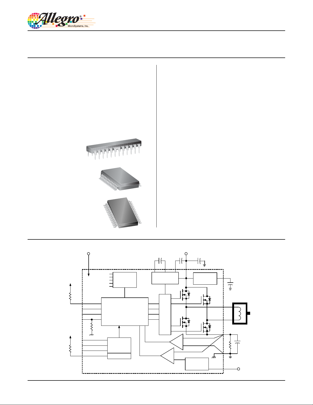
Packages:
Package B, 24-pin DIP
with exposed tabs
Package LB, 24-pin SOIC
with internally fused pins
Package LP, 28-pin TSSOP
with exposed thermal pad
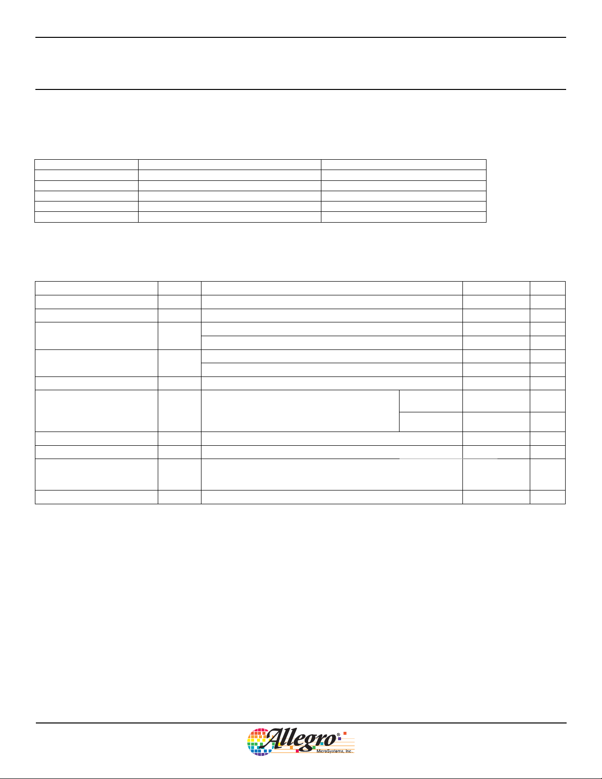
Description
Designed for pulse width modulated (PWM) current control of
DC motors, the A3959 is capable of output currents to ±3 A and
operating voltages to 50 V. Internal fixed off-time PWM currentcontrol timing circuitry can be adjusted via control inputs to
operate in slow, fast, and mixed current-decay modes.
PHASE and ENABLE input terminals are provided for use
in controlling the speed and direction of a DC motor with
externally applied PWM-control signals. Internal synchronous
rectification control circuitry is provided to reduce power
dissipation during PWM operation.
Internal circuit protection includes thermal shutdown with
hysteresis, undervoltage monitoring of supply and charge
pump, and crossover-current protection. Special power-up
sequencing is not required.
The A3959 provides a choice of three power packages, a 24-pin
DIP with batwing tabs (package suffix ‘B’), a 24-lead SOIC
with four internally-fused pins (package suffix ‘LB’), and a
thin (<1.2 mm) 28-pin TSSOP with an exposed thermal pad
(suffix ‘LP’). In all cases, the power pins and tabs are at ground
potential and need no electrical isolation. Each package is lead
(Pb) free, with 100% matte tin leadframes.
DD
TO V
SLEEP
EXT MODE
PHASE
ENABLE
TO V
DD
BLANK
PFD1
PFD2
ROSC
Not to scale
V
DD
LOGIC
SUPPLY
CHARGE PUMP
BANDGAP
V
C
REG
TSD
Functional Block Diagram
CP1
VOLTAGE &
DD
FAULT DETECT
CONTROL LOGIC
PWM
TIMER
OSC
UNDER-
CHARGE
PUMP
CURRENT
CP2
GATE DRIVE
SENSE
CP
ZERO
CURRENT
DETECT
V
BB
+
LOAD
SUPPLY
BANDGAP
REGULATOR
REFERENCE
BUFFER &
w10
V
REG
OUT
OUT
SENSE
REF
A
B
C
S
S
R
Dwg. FP-048-2A
V
REF
29319.37K
A3959
DMOS Full-Bridge PWM Motor Driver
Selection Guide
Part Number Package Packing
A3959SB-T 24-pin DIP with exposed tabs 15 per tube
A3959SLB-T 24-pin SOIC with internally fused pins 31 per tube
A3959SLBTR-T 24-pin SOIC with internally fused pins 1000 per reel
A3959SLP-T 28-pin TSSOP with exposed thermal pad 50 per tube
A3959SLPTR-T 28-pin TSSOP with exposed thermal pad 4000 per reel
Absolute Maximum Ratings
Characteristic Symbol Notes Rating Units
Load Supply Voltage V
Logic Supply Voltage V
Input Voltage V
Sense Voltage V
Reference Voltage V
Output Current I
Package Power Dissipation P
Operating Ambient Temperature T
Maximum Junction Temperature TJ(max)
Storage Temperature T
BB
DD
IN
REF
OUT
stg
Continuous –0.3 to V
tw < 30 ns –1.0 to V
Continuous 0.5 V
S
t
< 3 μs 2.5 V
w
Output current rating may be limited by duty cycle, am-
bient temperature, and heat sinking. Under any set of
conditions, do not exceed the specifi ed current rating
or a junction temperature of 150°C.
See Thermal Characteristics – –
D
Range S –20 to 85 ºC
A
Fault conditions that produce excessive junction temperature will activate
the device’s thermal shutdown circuitry. These conditions can be toler-
ated but should be avoided.
50 V
7.0 V
+ 0.3 V
DD
+ 1.0 V
DD
V
DD
Repetitive ±3.0 A
Peak, < 3 μs ±6.0 A
150 ºC
–55 to 150 ºC
V
Allegro MicroSystems, Inc.
115 Northeast Cutoff
Worcester, Massachusetts 01615-0036 U.S.A.
1.508.853.5000; www.allegromicro.com
2
A3959
0
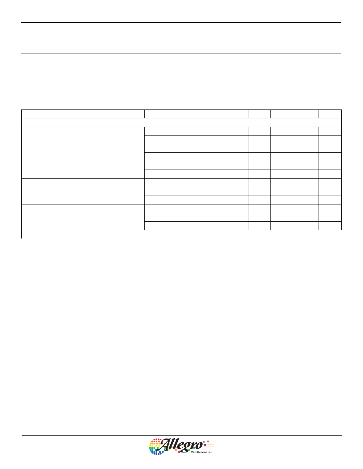
Thermal Characteristics
Characteristic Symbol Test Conditions Value Units
Package Power Dissipation P
Package Thermal Resistance, Junction
to Ambient
Package Thermal Resistance, Junction
to Tab
Package Thermal Resistance, Junction
to Pad
*Additional thermal information available on Allegro website.
D
R
θJA
R
θJT
R
θJP
DMOS Full-Bridge PWM Motor Driver
B package
LB package
LP package
1-layer PCB, minimal exposed copper area 54 ºC/W
B Package
LB Package
LP Package
B and LB packages 6 ºC/W
LP package 2 ºC/W
2-layer PCB, 1-in.2 2-oz copper exposed area 36 ºC/W
4-layer PCB, based on JEDEC standard 26 ºC/W
1-layer PCB, minimal exposed copper area 77 ºC/W
2-layer PCB, 1-in.2 2-oz copper exposed area 51 ºC/W
4-layer PCB, based on JEDEC standard 35 ºC/W
1-layer PCB, minimal exposed copper area 100 ºC/W
2-layer PCB, 1-in.2 2-oz copper exposed area 40 ºC/W
4-layer PCB, based on JEDEC standard 28 ºC/W
3.3 W
2.5 W
3.1 W
5
SUFFIX 'B', R
SUFFIX 'LP', R
4
SUFFIX 'LB', R
4-LAYER BOARD
QJA
QJA
QJA
= 26oC/W
= 28oC/W
= 35oC/W
3
2
1
SUFFIX 'B', R
SUFFIX 'LP', R
SUFFIX 'LB', R
2-LAYER BOARD,
1 SQ. IN. COPPER EA. SIDE
ALLOWABLE PACKAGE POWER DISSIPATION (W)
0
25
QJA
= 36oC/W
QJA
= 40oC/W
QJA
= 51oC/W
50 75 100 125 15
TEMPERATURE IN ooooC
Allegro MicroSystems, Inc.
115 Northeast Cutoff
Worcester, Massachusetts 01615-0036 U.S.A.
1.508.853.5000; www.allegromicro.com
3
A3959
DMOS Full-Bridge PWM Motor Driver
Allegro MicroSystems, Inc.
115 Northeast Cutoff
Worcester, Massachusetts 01615-0036 U.S.A.
1.508.853.5000; www.allegromicro.com
4
 Loading...