

Allegro A3958SLB, A3958SB Datasheet
3958
DMOS FULL-BRIDGE PWM
Data Sheet
29319.31
MOTOR DRIVER
A3958SLB
CP
1
CP2
2
CP1
PHASE
OSC
GROUND
GROUND
LOGIC SUPPLY
ENABLE
DATA
CLOCK
STROBE
3
4
5
6
7
8
9
9
10
11
12
θ
V
CC
CHARGE PUMP
V
LOGIC
÷
SERIAL PORT
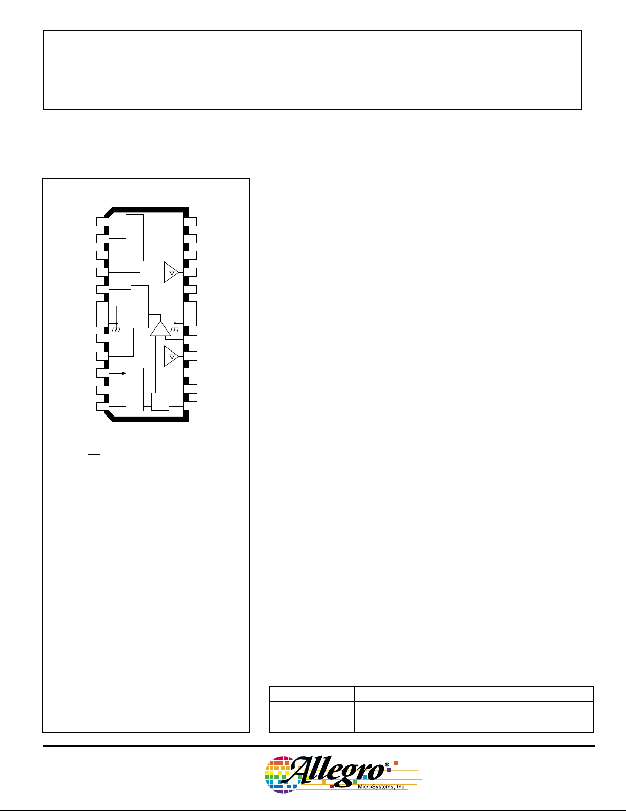
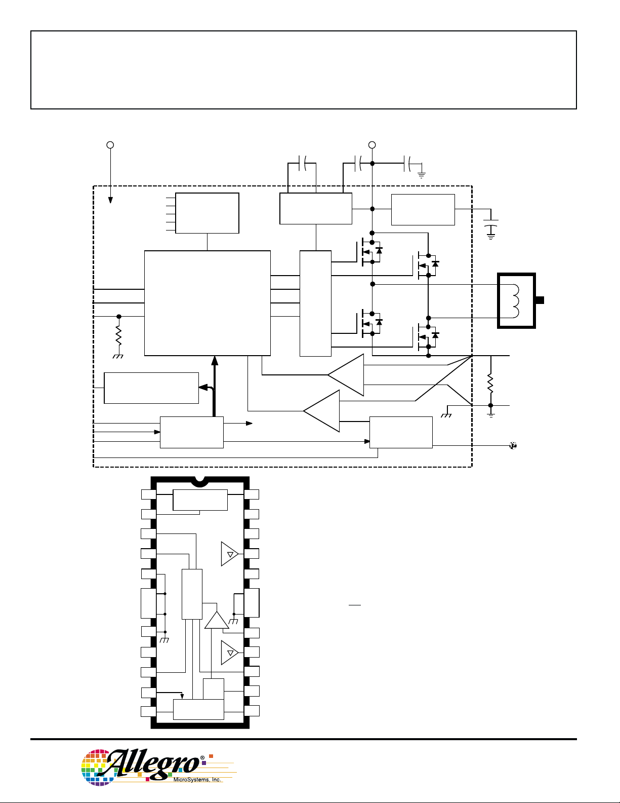
Note that the A3958SLB(SOIC) and A3958SB
(DIP) do not share a common terminal
assignment.
NC
BB
NC
V
24
RANGE
23
NO
22
CONNECTION
OUT
21
LOAD SUPPLY
20
GROUND
19
18
GROUND
SENSE
17
OUT
16
NO
15
CONNECTION
MODE
14
REF
13
REG
B
A
Dwg. PP-069
ABSOLUTE MAXIMUM RATINGS
Load Supply Voltage, VBB.................. 50 V
Output Current, I
Logic Supply Voltage, VDD................ 7.0 V
Input Voltage, VIN.... -0.3 V to VDD + 0.3 V
Sense Voltage, VS............................ 0.5 V
Reference Voltage, V
Package Power Dissipation (TA = 25°C), P
A3958SB ................................. 3.1 W*
A3958SLB ............................... 2.2 W*
Operating Temperature Range,
TA............................... -20°C to +85°C
Junction Temperature,
TJ............................................ +150°C
Storage Temperature Range,
TS............................. -55°C to +150°C
Output current rating may be limited by duty cycle,
ambient temperature, and heat sinking. Under any
set of conditions, do not exceed the specified
current rating or a junction temperature of 150°C.
* Per SEMI G42-88 Specification.
........................ ±2.0 A
OUT
.................. 2.7 V
REF
D
Designed for pulse-width modulated (PWM) current control of dc
motors, the A3958SB and A3958SLB are capable of continuous output
currents to ±2 A and operating voltages to 50 V. Internal fixed offtime PWM current-control timing circuitry can be programmed via a
serial interface to operate in slow, fast, and mixed current-decay
modes.
PHASE and ENABLE input terminals are provided for use in
controlling the speed and direction of a dc motor with externally
applied PWM-control signals. The ENABLE input can be
programmed via the serial port to PWM the bridge in fast or slow
current decay. Internal synchronous rectification control circuitry is
provided to reduce power dissipation during PWM operation.
Internal circuit protection includes thermal shutdown with
hysteresis, and crossover-current protection. Special power-up
sequencing is not required.
The A3958SB/SLB is supplied in a choice of two power
packages, a 24-pin plastic DIP with a copper batwing tab (package
suffix ‘B’), and a 24-lead plastic SOIC with a copper batwing tab
(package suffix ‘LB’). In both cases, the power tab is at ground
potential and needs no electrical isolation.
FEATURES
■ ±2 A, 50 V Continuous Output Rating
■ Low
■ Programmable Mixed, Fast, and Slow Current-Decay Modes
■ Serial Interface Controls Chip Functions
■ Synchronous Rectification for Low Power Dissipation
■ Internal UVLO and Thermal-Shutdown Circuitry
■ Crossover-Current Protection
Always order by complete part number:
r
Outputs (270 mΩ, Typical)
DS(on)
Part Number Package R
θJA
R
A3958SB 24-pin batwing DIP 40°C/W 6°C/W
A3958SLB 24-lead batwing SOIC 56°C/W 6°C/W
θJT
3958
DMOS FULL-BRIDGE
PWM MOTOR DRIVER
V
DD
LOGIC
SUPPLY
FUNCTIONAL BLOCK DIAGRAM
V
BB
CP1
CP2
CP
LOAD
SUPPLY
+
MODE
PHASE
ENABLE
OSC
CLOCK
DATA
STROBE
RANGE
CHARGE PUMP
BANDGAP
V
DD
C
REG
TSD
PROGRAMMABLE
PWM TIMER
UNDER-
VOLTAGE &
FAULT DETECT
CONTROL LOGIC
PHASE
ENABLE
FIXED OFF
BLANK
DECAY
SERIAL
PORT
SYNC RECT MODE
SYNC RECT DISABLE
PWM MODE INT
PWM MODE EXT
SLEEP
MODE
CHARGE
PUMP
GATE DRIVE
CURRENT
SENSE
ZERO
CURRENT
DETECT
RANGE
BANDGAP
REGULATOR
REFERENCE
BUFFER &
DIVIDER
V
REG
OUT
OUT
SENSE
REF
A
B
R
C
S
S
Dwg. FP-048
REF
V
CPCP2
1
CHARGE PUMP
CP1
2
PHASE
OSC
GROUND
GROUND
GROUND
GROUND
LOGIC
SUPPLY
ENABLE
DATA
CLOCK
θ
3
4
5
6
7
8
V
9
9
10
11
12
LOGIC
DD
÷
SERIAL PORT
2
24
V
REG
23
RANGE
22
OUT
21
V
BB
20
19
18
17
16
15
14
13
B
LOAD
SUPPLY
GROUND
GROUND
SENSE
A
OUT
MODE
REF
STROBE
Dwg. PP-069-1
A3958SB
Note that the A3958SLB (SOIC) and A3958SB
(DIP) do
assignment.
not share a common terminal
115 Northeast Cutoff, Box 15036
Worcester, Massachusetts 01615-0036 (508) 853-5000
Copyright © 2000, Allegro MicroSystems, Inc.

3958
DMOS FULL-BRIDGE
PWM MOTOR DRIVER
ELECTRICAL CHARACTERISTICS at TA = +25°C, VBB = 50 V, VDD = 5.0 V, V
f
< 50 kHz (unless noted otherwise)
PWM
SENSE
= 0.5 V,
Limits
Characteristics Symbol Test Conditions Min. Typ. Max. Units
Output Drivers
Load Supply Voltage Range V
BB
Operating 20 – 50 V
During sleep mode 0 – 50 V
Output Leakage Current I
Output On Resistance r
DS(on)
Body Diode Forward Voltage V
DSS
V
= V
OUT
V
OUT
Source driver, I
Sink driver, I
Source diode, IF = -2 A – 1.2 1.6 V
F
BB
= 0 V – <-1.0 -20 µA
= -2 A – 270 300 mΩ
OUT
= 2 A – 270 300 mΩ
OUT
– <1.0 20 µA
Sink diode, IF = 2 A – 1.2 1.6 V
Load Supply Current I
BB
f
< 50 kHz – 4.0 7.0 mA
PWM
Charge pump on, outputs disabled – 2.0 5.0 mA
Sleep Mode – – 20 µA
Control Logic
Logic Supply Voltage Range V
Logic Input Voltage V
V
Logic Input Current I
(all inputs except ENABLE)
I
ENABLE Input Current I
I
OSC input frequency f
OSC input duty cycle dc
DD
IN(1)
IN(0)
IN(1)
IN(0)
IN(1)
IN(0)
OSC
OSC
Operating 4.5 5.0 5.5 V
2.0 – – V
––0.8V
VIN = 2.0 V – <1.0 20 µA
VIN = 0.8 V – <-2.0 -20 µA
VIN = 2.0 V – 40 100 µA
VIN = 0.8 V – – 0 µA
Operating 2.9 – 6.1 MHz
Operating 40 – 60 %
OSC input hysteresis – Operating 200 – 400 mV
Input Hysterisis – All digital inputs except OSC 50 – 100 mV
Reference Input Volt. Range V
Reference Input Current I
Comparator Input Offset Volt. V
REF
REF
IO
Operating 0.0 – 2.6 V
V
= 2.5 V – – ±0.5 µA
REF
V
= 0 V – 0 ±5.0 mV
REF
Continued next page …
www.allegromicro.com
3

3958
DMOS FULL-BRIDGE
PWM MOTOR DRIVER
ELECTRICAL CHARACTERISTICS at TA = +25°C, VBB = 50 V, VDD = 5.0 V, V
f
< 50 kHz (unless noted otherwise), continued.
PWM
SENSE
= 0.5 V,
Limits
Characteristics Symbol Test Conditions Min. Typ. Max. Units
Control Logic
Buffer Input Offset Volt. V
IO
–0±15 mV
Reference Divider Ratio – D14 = High 9.9 10 10.2 –
D14 = Low 4.95 5.0 5.05 –
Propagation Delay Times t
pd
PWM change to source ON – 600 – ns
PWM change to source OFF – 100 – ns
PWM change to sink ON – 600 – ns
PWM change to sink OFF – 100 – ns
Phase change to sink ON – 600 – ns
Phase change to sink OFF – 100 – ns
Phase change to source ON – 600 – ns
Phase change to source OFF – 100 – ns
Thermal Shutdown Temp. T
Thermal Shutdown Hysteresis ∆T
J
J
UVLO Enable Threshold UVLO Increasing V
DD
– 165 – °C
–15– °C
3.90 4.2 4.45 V
UVLO Hysteresis ∆UVLO 0.05 0.10 – V
Logic Supply Current I
DD
f
< 50 kHz – 6.0 10 mA
PWM
Sleep Mode, Inputs < 0.5 V – – 2.0 mA
NOTES: 1. Typical Data is for design information only.
2. Negative current is defined as coming out of (sourcing) the specified device terminal.
4
115 Northeast Cutoff, Box 15036
Worcester, Massachusetts 01615-0036 (508) 853-5000
 Loading...