

Allegro A3955SLB, A3955SB Datasheet
1
PFD
2
REF
3
RC
GROUND
GROUND
LOGIC
SUPPLY
PHASE
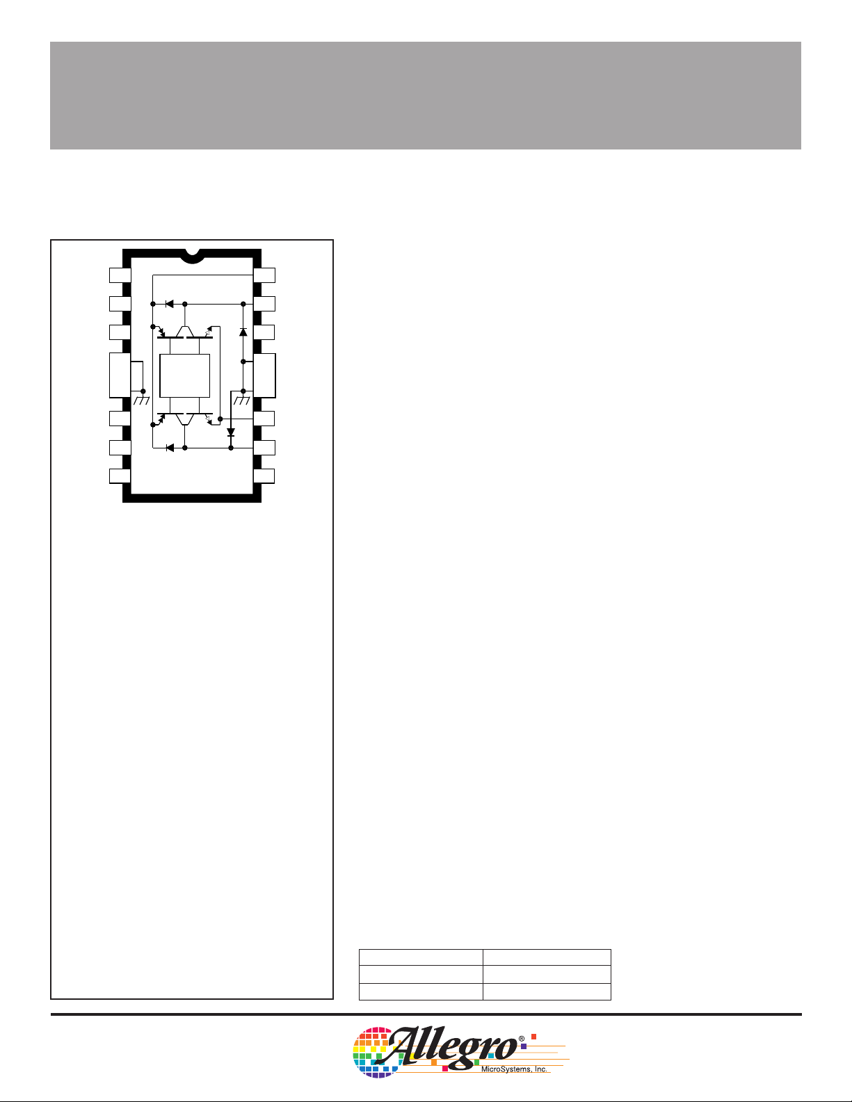
Note the A3955SB (DIP) and the A3955SLB
(SOIC) are electrically identical and share a
common terminal number assignment.
4
5
6
V
CC
7
D
8
2
LOGIC
V
BB
LOAD
16
SUPPLY
OUT
15
D
14
GROUND
13
12
GROUND
11
SENSE
OUT
10
9
D
Dwg. PP-056-2
Data Sheet
29319.41
3955
FULL-BRIDGE PWM
MICROSTEPPING MOTOR DRIVER
The A3955SB and A3955SLB are designed for driving one winding
of a bipolar stepper motor in a microstepping mode. The outputs are
rated for continuous output currents to ±1.5 A and operating voltages
B
0
A
1
to 50 V. Internal pulse-width modulated (PWM) current control combined with an internal three-bit nonlinear digital-to-analog converter
allows the motor current to be controlled in full-, half-, quarter-, or
eighth-step (microstepping) modes. Nonlinear increments minimize
the number of control lines necessary for microstepping.
Microstepping provides for increased step resolution, and reduces
torque variations and resonance problems at low speed.
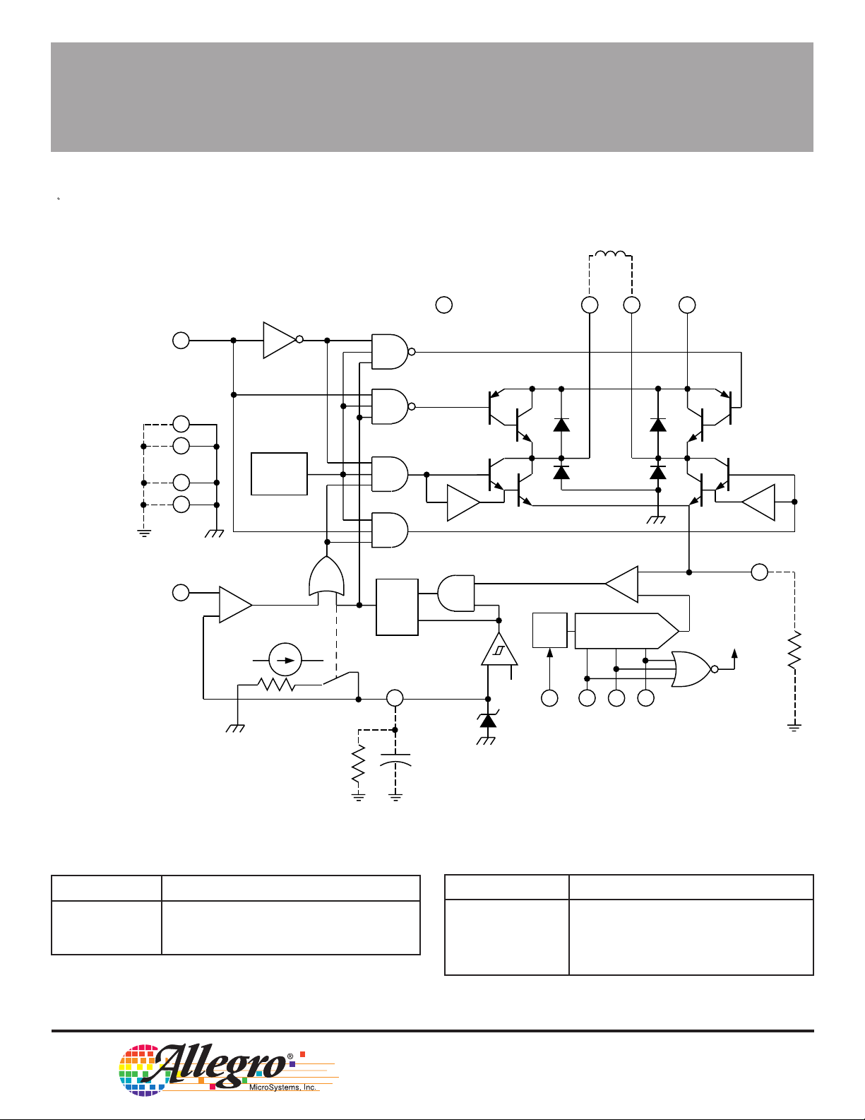
Internal circuitry determines whether the PWM current-control
circuitry operates in a slow (recirculating) current-decay mode, fast
(regenerative) current-decay mode, or in a mixed current-decay mode
in which the off time is divided into a period of fast current decay with
the remainder of the fixed off time spent in slow current decay. The
combination of user-selectable current-sensing resistor and reference
voltage, digitally selected output current ratio; and slow, fast, or mixed
current-decay modes provides users with a broad, variable range of
motor control.
ABSOLUTE MAXIMUM RATINGS
Load Supply Voltage, VBB. . . . . . . . . . 50 V
Output Current, I
(Continuous) . . . . . . . . . . . . . . ±1.5 A*
Logic Supply Voltage, V
Logic/Reference Input Voltage Range,
V
. . . . . . . . . . . -0.3 V to VCC + 0.3 V
IN
Sense Voltage, V
Package Power Dissipation,
P
. . . . . . . . . . . . . . . . . . . . See Graph
D
Operating Temperature Range,
T
. . . . . . . . . . . . . . . . . -20˚C to +85˚C
A
Junction Temperature, T
Storage Temperature Range,
T
. . . . . . . . . . . . . . . . -55˚C to +150˚C
S
* Output current rating may be limited by duty
cycle, ambient temperature, and heat sinking.
Under any set of conditions, do not exceed the
specified current rating or a junction temperature
of 150˚C.
† Fault conditions that produce excessive junction
temperature will activate the device’s thermal
shutdown circuitry. These conditions can be
tolerated but should be avoided.
OUT
. . . . . . . . . 7.0 V
CC
. . . . . . . . . . . . . . . . 1.0 V
S
. . . . . . . +150˚C†
J
Internal circuit protection includes thermal shutdown with hysteresis, transient-suppression diodes, and crossover current protection.
Special power-up sequencing is not required.
The A3955S— is supplied in a choice of two power packages; a
16-pin dual-in-line plastic package with copper heat-sink tabs (suffix
‘B’), and a 16-lead plastic SOIC with copper heat-sink tabs (suffix ‘LB’).
For both package styles, the power tab is at ground potential and
needs no electrical isolation.
FEATURES
■ ±1.5 A Continuous Output Current
■ 50 V Output Voltage Rating
■ Internal PWM Current Control
■ 3-Bit Non-Linear DAC
■ Fast, Mixed Fast/Slow, and Slow Current-Decay Modes
■ Internal Transient-Suppression Diodes
■ Internal Thermal-Shutdown Circuitry
■ Crossover-Current and UVLO Protection
Always order by complete part number:
Part Number Package
A3955SB 16-Pin DIP
A3955SLB 16-Lead SOIC
3955
9
2814
6
7
16
10
15
1
4
5
11
12
13
3
FULL-BRIDGE PWM
MICROSTEPPING
MOTOR DRIVER
FUNCTIONAL BLOCK DIAGRAM
PHASE
GROUND
PFD
UVLO
& TSD
MIXED-DECAY
COMPARATOR
+
–
BLANKING
V
CC
R
T
PWM LATCH
R
Q
S
RC
C
T
LOGIC
SUPPLY
V
CC
BLANKING
GATE
+ –
A
OUT
V
BB
CURRENT-SENSE
COMPARATOR
÷3
V
TH
REF
D/A
2
D
B
OUT
LOAD
SUPPLY
SENSE
+
–
DISABLE
R
S
1
0
D
D
Table 1 — PHASE Truth Table
PHASE OUT
A
HH L
LL H
OUT
B
115 Northeast Cutoff, Box 15036
Worcester, Massachusetts 01615-0036 (508) 853-5000
W
Copyright © 1997 Allegro MicroSystems, Inc.
Table 2 — PFD Truth Table
V
PFD
≥3.5 V Slow Current-Decay Mode
1.1 V to 3.1 V Mixed Current-Decay Mode
≤0.8 V Fast Current-Decay Mode
Description
Dwg. FP-042

3955
FULL-BRIDGE PWM
MICROSTEPPING
MOTOR DRIVER
5
R = 6.0°C/W
θJT
4
D
2
Table 3 — DAC Truth Table
DAC DATA Current
D
D
1
0
Ratio, % V
REF/VS
H H H 100 3.00
3
2
SUFFIX 'B', R = 43°C/W
θJA
H H L 92.4 3.25
H L H 83.1 3.61
H L L 70.7 4.24
L H H 55.5 5.41
1
SUFFIX 'LB', R = 63°C/W
0
25
ALLOWABLE PACKAGE POWER DISSIPATION IN WATTS
50 75 100 125 150
θJA
TEMPERATURE IN °C
Dwg. GP-049-2A
L H L 38.2 7.85
L L H 19.5 15.38
L L L All Outputs Disabled
where VS = I
TRIP•RS
. See Applications section.
ELECTRICAL CHARACTERISTICS at TA = 25˚C, VBB = 5 V to 50 V, VCC = 4.5 V to 5.5 V
(unless otherwise noted.)
Limits
Characteristic Symbol Test Conditions Min. Typ. Max. Units
Power Outputs
Load Supply Voltage Range V
Output Leakage Current I
Output Saturation Voltage V
CE(SAT)
(Forward or Reverse Mode)
Sense Current Offset I
Clamp Diode Forward Voltage V
(Sink or Source)
Motor Supply Current I
(No Load)
BB(ON)
I
BB(OFF)
BB
CEX
SO
Operating, I
V
= V
OUT
V
= 0 V — <-1.0 -50 µA
OUT
= ±1.5 A, L = 3 mH V
OUT
BB
CC
—50 V
— <1.0 50 µA
VS = 1.0 V:
Source Driver, I
Source Driver, I
Sink Driver, I
Sink Driver, I
IS - I
OUT
, I
OUT
= 850 mA, 20 33 40 mA
= -0.85 A — 1.0 1.2 V
OUT
= -1.5 A — 1.3 1.5 V
OUT
= 0.85 A — 0.5 0.6 V
OUT
= 1.5 A — 1.3 1.5 V
OUT
VS = 0 V, VCC = 5 V
F
IF = 0.85 A — 1.2 1.4 V
I
= 1.5 A — 1.4 1.7 V
F
— 2.0 4.0 mA
D0 = D1 = D2 = 0.8 V — 1.0 50 µA
Continued next page…
3955
FULL-BRIDGE PWM
MICROSTEPPING
MOTOR DRIVER
ELECTRICAL CHARACTERISTICS at TA = 25˚C, VBB = 5 V to 50 V, VCC = 4.5 V to 5.5 V
(unless otherwise noted. )
Limits
Characteristic Symbol Test Conditions Min. Typ. Max. Units
Control Circuitry
Logic Supply Voltage Range V
Reference Voltage Range V
CC
REF
UVLO Enable Threshold VCC = 0 → 5 V 3.35 3.70 4.05 V
UVLO Hysteresis 0.30 0.45 0.60 V
Logic Supply Current I
Logic Input Voltage V
Logic Input Current I
Mixed-Decay Comparator V
CC(ON)
I
CC(OFF)
IN(1)
V
IN(0)
IN(1)
I
IN(0)
PFD
Trip Points
Mixed-Decay Comparator V
IO(PFD)
Input Offset Voltage
Mixed-Decay Comparator ∆V
IO(PFD)
Hysteresis
Reference Input Current I
Reference Divider Ratio V
REF
REF/VS
Digital-to-Analog Converter — 1.0 V < V
Accuracy*
Current-Sense Comparator V
IO(S)
Input Offset Voltage*
Operating 4.5 5.0 5.5 V
Operating 0.5 — 2.5 V
—4250mA
D0 = D1 = D2 = 0.8 V — 12 16 mA
2.0 — — V
— — 0.8 V
V
= 2.0 V — <1.0 20 µA
IN
V
= 0.8 V — <-2.0 -200 µA
IN
Slow Current-Decay Mode 3.5 — — V
Mixed Current-Decay Mode 1.1 — 3.1 V
Fast Current-Decay Mode — — 0.8 V
—0±20 mV
5.0 25 55 mV
V
= 0 V to 2.5 V — — ±5.0 µA
REF
at trip, D0 = D1 = D2 = 2 V — 3.0 — —
≤ 2.5 V — — ±3.0 %
REF
0.5 V < V
V
REF
≤ 1.0 V — — ±4.0 %
REF
= 0 V — — ±5.0 mV
Step Reference SRCR D
Current Ratio
* The total error for the V
function is the sum of the D/A error and the current-sense comparator input offset voltage.
REF/VS
= D1 = D2 = 0.8 V — 0 — %
0
D
= 2 V, D1 = D2 = 0.8 V — 19.5 — %
0
= 0.8 V, D1 = 2 V, D2 = 0.8 V — 38.2 — %
D
0
= D1 = 2 V, D2 = 0.8 V — 55.5 — %
D
0
= D1 = 0.8 V, D2 = 2 V — 70.7 — %
D
0
= 2 V, D1 = 0.8 V, D2 = 2 V — 83.1 — %
D
0
= 0.8 V, D1 = D2 = 2 V — 92.4 — %
D
0
D
= D1 = D2 = 2 V — 100 — %
0
Continued next page…
115 Northeast Cutoff, Box 15036
Worcester, Massachusetts 01615-0036 (508) 853-5000
3955
FULL-BRIDGE PWM
MICROSTEPPING
MOTOR DRIVER
ELECTRICAL CHARACTERISTICS at TA = 25˚C, VBB = 5 V to 50 V, VCC = 4.5 V to 5.5 V
(unless otherwise noted.)
Limits
Characteristic Symbol Test Conditions Min. Typ. Max. Units
Control Circuitry (cont’d)
Thermal Shutdown Temp. T
Thermal Shutdown Hysteresis ∆T
AC Timing
J
J
— 165 — °C
—15—°C
PWM RC Fixed Off-time t
PWM Turn-Off Time t
PWM Turn-On Time t
PWM Minimum On Time t
Crossover Dead Time t
OFF RC
PWM(OFF)
PWM(ON)
ON(min)
CODT
CT = 470 pF, RT= 43 kΩ 18.2 20.2 22.3 µs
Current-Sense Comparator Trip — 1.0 1.5 µs
to Source OFF, I
Current-Sense Comparator Trip — 1.4 2.5 µs
to Source OFF, I
IRC Charge ON to Source ON, — 0.4 0.7 µs
I
= 100 mA
OUT
Charge ON to Source ON, — 0.55 0.85 µs
I
RC
I
= 1.5 A
OUT
VCC = 5.0 V, RT ≥ 43 kΩ, CT = 470 pF 1.0 1.6 2.2 µs
I
= 100 mA
OUT
1 kΩ Load to 25 V 0.3 1.5 3.0 µs
= 100 mA
OUT
= 1.5 A
OUT
 Loading...