

Allegro A3953SLB, A3953SB Datasheet
LOAD
BRAKE
1
2
REF
3
RC
GROUND
GROUND
SUPPLY
ENABLE
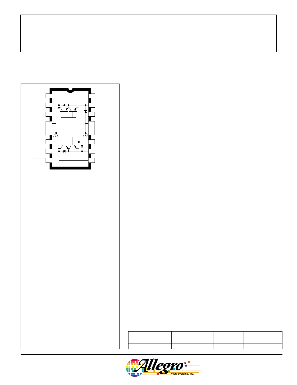
Note the A3953SB (DIP) and the A3953SLB
(SOIC) are electrically identical and share a
common terminal number assignment.
4
5
LOGIC
PHASE
V
6
CC
7
89
LOGIC
V
BB
V
BB
16
SUPPLY
15
OUT
14
MODE
13
GROUND
12
GROUND
11
SENSE
10
OUT
LOAD
SUPPLY
Dwg. PP-056
3953
FULL-BRIDGE PWM MOTOR DRIVER
Designed for bidirectional pulse-width modulated (PWM) current control
of inductive loads, the A3953S— is capable of continuous output currents to
±1.3 A and operating voltages to 50 V. Internal fixed off-time PWM current-
B
A
control circuitry can be used to regulate the maximum load current to a
desired value. The peak load current limit is set by the user’s selection of an
input reference voltage and external sensing resistor. The fixed off-time pulse
duration is set by a user- selected external RC timing network. Internal circuit
protection includes thermal shutdown with hysteresis, transient-suppression
diodes, and crossover current protection. Special power-up sequencing is not
required.
With the ENABLE input held low, the PHASE input controls load current
polarity by selecting the appropriate source and sink driver pair. The MODE
input determines whether the PWM current-control circuitry operates in a
slow current-decay mode (only the selected source driver switching) or in a
fast current-decay mode (selected source and sink switching). A userselectable blanking window prevents false triggering of the PWM currentcontrol circuitry. With the ENABLE input held high, all output drivers are
disabled. A sleep mode is provided to reduce power consumption.
Data Sheet
29319.8*
ABSOLUTE MAXIMUM RATINGS
Load Supply Voltage, VBB. . . . . . . . . . 50 V
Output Current, I
(Continuous) . . . . . . . . . . . . . . ±1.3 A*
Logic Supply Voltage, V
Logic/Reference Input Voltage Range,
. . . . . . . . . . . -0.3 V to VCC + 0.3 V
V
IN
Sense Voltage, V
(VCC = 5.0 V) . . . . . . . . . . . . . . . . 1.0 V
(V
= 3.3 V) . . . . . . . . . . . . . . . . 0.4 V
CC
Package Power Dissipation,
P
. . . . . . . . . . . . . . . . . . . . See Graph
D
Operating Temperature Range,
T
. . . . . . . . . . . . . . . . . -20˚C to +85˚C
A
Junction Temperature, T
Storage Temperature Range,
. . . . . . . . . . . . . . . . -55˚C to +150˚C
T
S
* Output current rating may be limited by duty
cycle, ambient temperature, and heat sinking.
Under any set of conditions, do not exceed the
specified current rating or a junction temperature
of 150˚C.
† Fault conditions that produce excessive junction
temperature will activate the device’s thermal
shutdown circuitry. These conditions can be
tolerated but should be avoided.
OUT
SENSE
. . . . . . . . . 7.0 V
CC
. . . . . . . +150˚C†
J
When a logic low is applied to the BRAKE input, the braking function is
enabled. This overrides ENABLE and PHASE to turn off both source drivers
and turn on both sink drivers. The brake function can be used to dynamically
brake brush dc motors.
The A3953S— is supplied in a choice of two power packages; a 16-pin
dual-in-line plastic package with copper heat-sink tabs, and a 16-lead plastic
SOIC with copper heat-sink tabs. For both package styles, the power tab is at
ground potential and needs no electrical isolation.
FEATURES
■ ±1.3 A Continuous Output Current
■ 50 V Output Voltage Rating
■ 3 V to 5.5 V Logic Supply Voltage
■ Internal PWM Current Control
■ Saturated Sink Drivers (Below 1 A)
■ Fast and Slow Current-Decay Modes
■ Automotive Capable
Always order by complete part number:
Part Number Package R
A3953SB 16-Pin DIP 43°C/W 6°C/W
A3953SLB 16-Lead SOIC 67°C/W 6°C/W
■ Sleep (Low Current
Consumption) Mode
■ Internal TransientSuppression Diodes
■ Internal ThermalShutdown Circuitry
■ Crossover-Current
and UVLO Protection
θJA
R
θJT
3953
FULL-BRIDGE
PWM MOTOR DRIVER
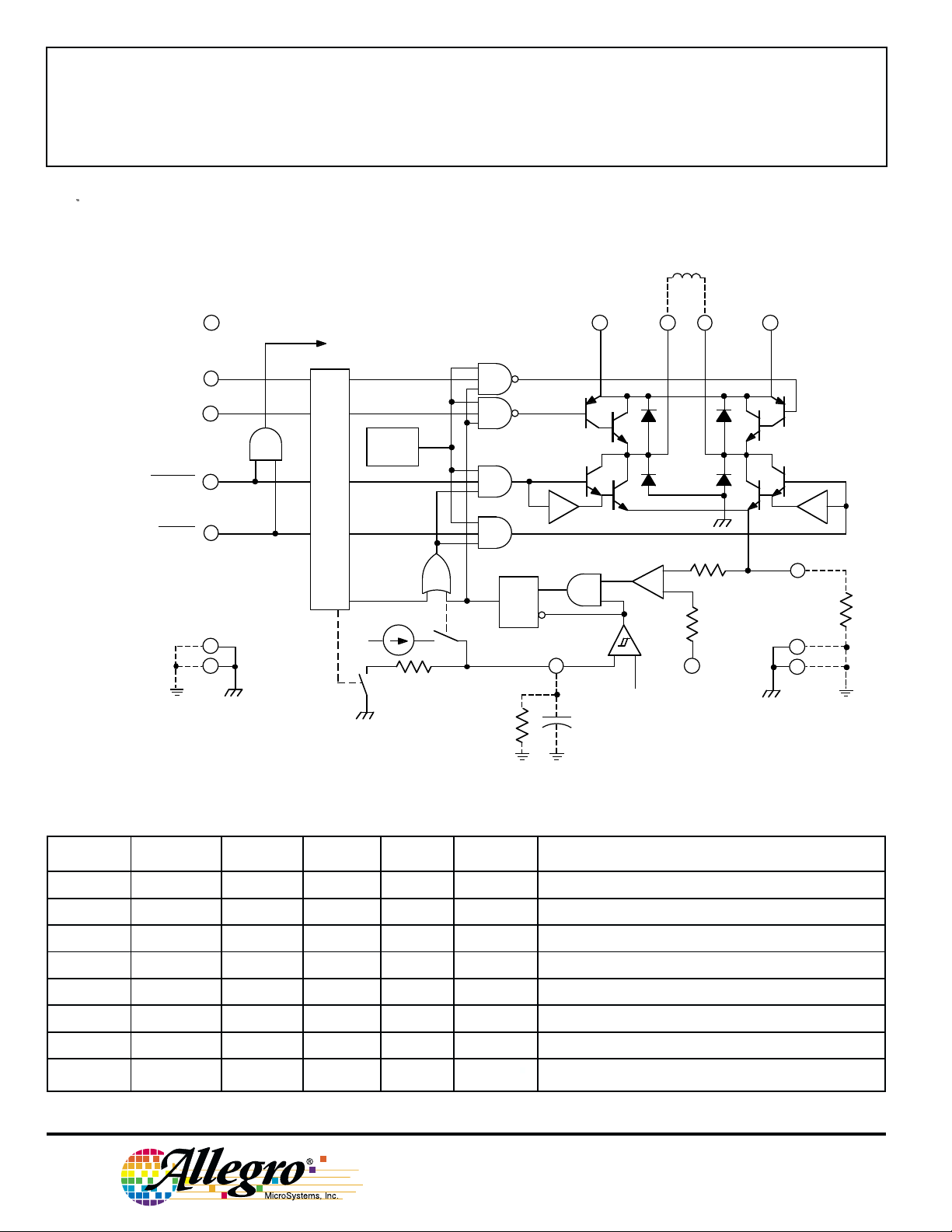
FUNCTIONAL BLOCK DIAGRAM
LOGIC
SUPPLY
MODE
PHASE
ENABLE
BRAKE
GROUND
A
+ –
OUT
10
V
+
–
V
TH
LOAD
V
6
CC
14
7
8
1
4
5 13
SLEEP &
STANDBY MODES
UVLO
& TSD
INPUT LOGIC
BLANKING
V
CC
PWM LATCH
R
Q
S
R
T
RC
3
SUPPLY
9
C
T
BB
2
REF
B
OUT
LOAD
15
SUPPLY
16
SENSE
GROUND
11
R
S
12
TRUTH TABLE
BRAKE ENABLE PHASE MODE OUT
A
H H X H Off Off Sleep Mode
H H X L Off Off Standby
H L H H H L Forward, Fast Current-Decay Mode
H L H L H L Forward, Slow Current-Decay Mode
H L L H L H Reverse, Fast Current-Decay Mode
H L L L L H Reverse, Slow Current-Decay Mode
L X X H L L Brake, Fast Current-Decay Mode
L X X L L L Brake, No Current Control
X = Irrelevant
2
115 Northeast Cutoff, Box 15036
Worcester, Massachusetts 01615-0036 (508) 853-5000
Copyright © 1995, 2000 Allegro MicroSystems, Inc.
OUT
B
DESCRIPTION
Dwg. FP-036-2A

3953
FULL-BRIDGE
PWM MOTOR DRIVER
5
R = 6.0°C/W
θJT
4
3
2
1
0
25
ALLOWABLE PACKAGE POWER DISSIPATION IN WATTS
SUFFIX 'B', R = 43°C/W
SUFFIX 'LB', R = 63°C/W
50 75 100 125 150
TEMPERATURE IN °C
θJA
θJA
Dwg. GP-049-2A
ELECTRICAL CHARACTERISTICS at TJ = 25˚C, VBB = 5 V to 50 V, VCC = 3.0 V to 5.5 V
(unless otherwise noted.)
Limits
Characteristic Symbol Test Conditions Min. Typ. Max. Units
Power Outputs
Load Supply Voltage Range V
Output Leakage Current I
Sense Current Offset I
Output Saturation Voltage V
BB
CEX
SO
CE(SAT)
BRAKE = H Source Driver, I
(Forward/Reverse Mode) Source Driver, I
Output Saturation Voltage V
CE(SAT)
BRAKE = L Sink Driver, I
(Brake Mode) Sink Driver, I
Clamp Diode Forward Voltage V
F
(Sink or Source) IF = 1.3 A — 1.4 1.6 V
Operating, I
V
= V
OUT
V
= 0 V — <-1.0 -50 µA
OUT
I
- I
SENSE
V
SENSE
V
= 0.4 V, VCC = 3.0 V:
SENSE
Sink Driver, I
Sink Driver, I
V
= 0.4 V, VCC = 3.0 V:
SENSE
= ±1.3 A, L = 3 mH V
OUT
BB
, I
OUT1
= 850 mA, 22 33 38 mA
OUT
= 0 V, VCC = 5 V
= -0.85 A — 1.0 1.1 V
OUT
= -1.3 A — 1.7 1.9 V
OUT
= 0.85 A — 0.4 0.5 V
OUT
= 1.3 A — 1.1 1.3 V
OUT
= 0.85 A — 1.0 1.2 V
OUT
= 1.3 A — 1.3 1.5 V
OUT
CC
— 50 V
— <1.0 50 µA
IF = 0.85 A — 1.2 1.4 V
www.allegromicro.com
Continued next page…
3

3953
FULL-BRIDGE
PWM MOTOR DRIVER
ELECTRICAL CHARACTERISTICS at TJ = 25˚C, VBB = 5 V to 50 V, VCC = 3.0 V to 5.5 V
(unless otherwise noted.)
Limits
Characteristic Symbol Test Conditions Min. Typ. Max. Units
AC Timing
PWM RC Fixed Off-time t
PWM Turn-Off Time t
PWM Turn-On Time t
PWM(OFF)
PWM(ON)
PWM Minimum On Time t
Propagation Delay Times t
OFF RC
ON(min)
pd
CT = 680 pF, RT= 30 kΩ, VCC = 3.3 V 18.3 20.4 22.5 µs
Comparator Trip to Source Off, — 1.0 1.5 µs
I
= 25 mA
OUT
Comparator Trip to Source Off, — 1.8 2.6 µs
I
= 1.3 A
OUT
IRC Charge On to Source On, — 0.4 0.7 µs
I
= 25 mA
OUT
IRC Charge On to Source On, — 0.55 0.85 µs
I
= 1.3 A
OUT
VCC = 3.3 V, RT ≥ 12 kΩ, CT = 680 pF 0.8 1.4 1.9 µs
VCC = 5.0 V, RT ≥ 12 kΩ, CT = 470 pF 0.8 1.6 2.0 µs
I
= ±1.3 A, 50% to 90%:
OUT
ENABLE On to Source On — 1.0 — µs
ENABLE Off to Source Off — 1.0 — µs
ENABLE On to Sink On — 1.0 — µs
ENABLE Off to Sink Off
(MODE = L)
— 0.8 — µs
PHASE Change to Sink On — 2.4 — µs
PHASE Change to Sink Off — 0.8 — µs
PHASE Change to Source On — 2.0 — µs
Crossover Dead Time t
Maximum PWM Frequency f
4
CODT
PWM(max)
PHASE Change to Source Off — 1.7 — µs
1 kΩ Load to 25 V, VBB = 50 V 0.3 1.5 3.0 µs
I
= 1.3 A 70 ——kHz
OUT
Continued next page…
115 Northeast Cutoff, Box 15036
Worcester, Massachusetts 01615-0036 (508) 853-5000
3953
FULL-BRIDGE
PWM MOTOR DRIVER
ELECTRICAL CHARACTERISTICS at TJ = 25˚C, VBB = 5 V to 50 V, VCC = 3.0 V to 5.5 V
(unless otherwise noted. )
Limits
Characteristic Symbol Test Conditions Min. Typ. Max. Units
Control Circuitry
Thermal Shutdown Temp. T
Thermal Shutdown Hysteresis ∆T
J
J
— 165 — °C
— 8.0 — °C
UVLO Enable Threshold 2.5 2.75 3.0 V
UVLO Hysteresis 0.12 0.17 0.25 V
Logic Supply Current I
Motor Supply Current I
(No Load) I
CC(ON)
I
CC(OFF)
I
CC(Brake)
I
CC(Sleep)
BB(ON)
BB(OFF)
I
BB(Brake)
I
BB(Sleep)
Logic Supply Voltage Range V
Logic Input Voltage V
V
Logic Input Current I
V
Voltage Range V
SENSE
SENSE(3.3)
V
SENSE(5.0)
Reference Input Current I
Comparator Input Offset Volt. V
IN(1)
I
IN(0)
REF
CC
IN(1)
IN(0)
IO
V
V
V
V
V
V
V
V
= 0.8 V, V
ENABLE
= 2.0 V, V
ENABLE
= 0.8 V — 42 50 mA
BRAKE
= V
ENABLE
ENABLE
ENABLE
BRAKE
ENABLE
MODE
= 0.8 V — 2.5 4.0 mA
= 2.0 V, V
= 0.8 V — 1.0 50 µA
= V
MODE
= 2.0 V — 42 50 mA
BRAKE
= 0.8 V — 12 15 mA
MODE
= V
MODE
= 2.0 V — 500 800 µA
BRAKE
= 0.8 V — 1.0 50 µA
= 2.0 V — 1.0 50 µA
Operating 3.0 5.0 5.5 V
2.0 —— V
——0.8 V
V
= 2.0 V — <1.0 20 µA
IN
V
= 0.8 V — <-2.0 -200 µA
IN
V
= 3.0 V to 3.6 V 0 — 0.4 V
CC
V
= 4.5 V to 5.5 V 0 — 1.0 V
CC
V
= 0 V to 1 V ——±5.0 µA
REF
V
= 0 V — ±2.0 ±5.0 mV
REF
www.allegromicro.com
5
 Loading...