

Allegro A3952KEB, A3952KB, A3952SW, A3952SLB, A3952SEB Datasheet
...
Data Sheet
29319.1*
FULL-BRIDGE PWM MOTOR DRIVER
Designed for bidirectional pulse-width modulated current control of
inductive loads, the A3952S– is capable of continuous output currents
to ±2 A and operating voltages to 50 V. Internal fixed off-time PWM
current-control circuitry can be used to regulate the maximum load
current to a desired value. The peak load current limit is set by the
user’s selection of an input reference voltage and external sensing
resistor. The fixed OFF-time pulse duration is set by a user-selected
external RC timing network. Internal circuit protection includes thermal
shutdown with hysteresis, transient suppression diodes, and crossovercurrent protection. Special power-up sequencing is not required.
With the ENABLE input held low, the PHASE input controls load
current polarity by selecting the appropriate source and sink driver pair.
The MODE input determines whether the PWM current-control circuitry
operates in a slow current-decay mode (only the selected sink driver
switching) or in a fast current-decay mode (selected source and sink
switching). A user-selectable blanking window prevents false triggering
of the PWM current control circuitry. With the ENABLE input held high,
all output drivers are disabled. A sleep mode is provided to reduce
power consumption when inactive.
When a logic low is applied to the BRAKE input, the braking
function is enabled. This overrides ENABLE and PHASE to turn OFF
both source drivers and turn ON both sink drivers. The brake function
can be safely used to dynamically brake brush dc motors.
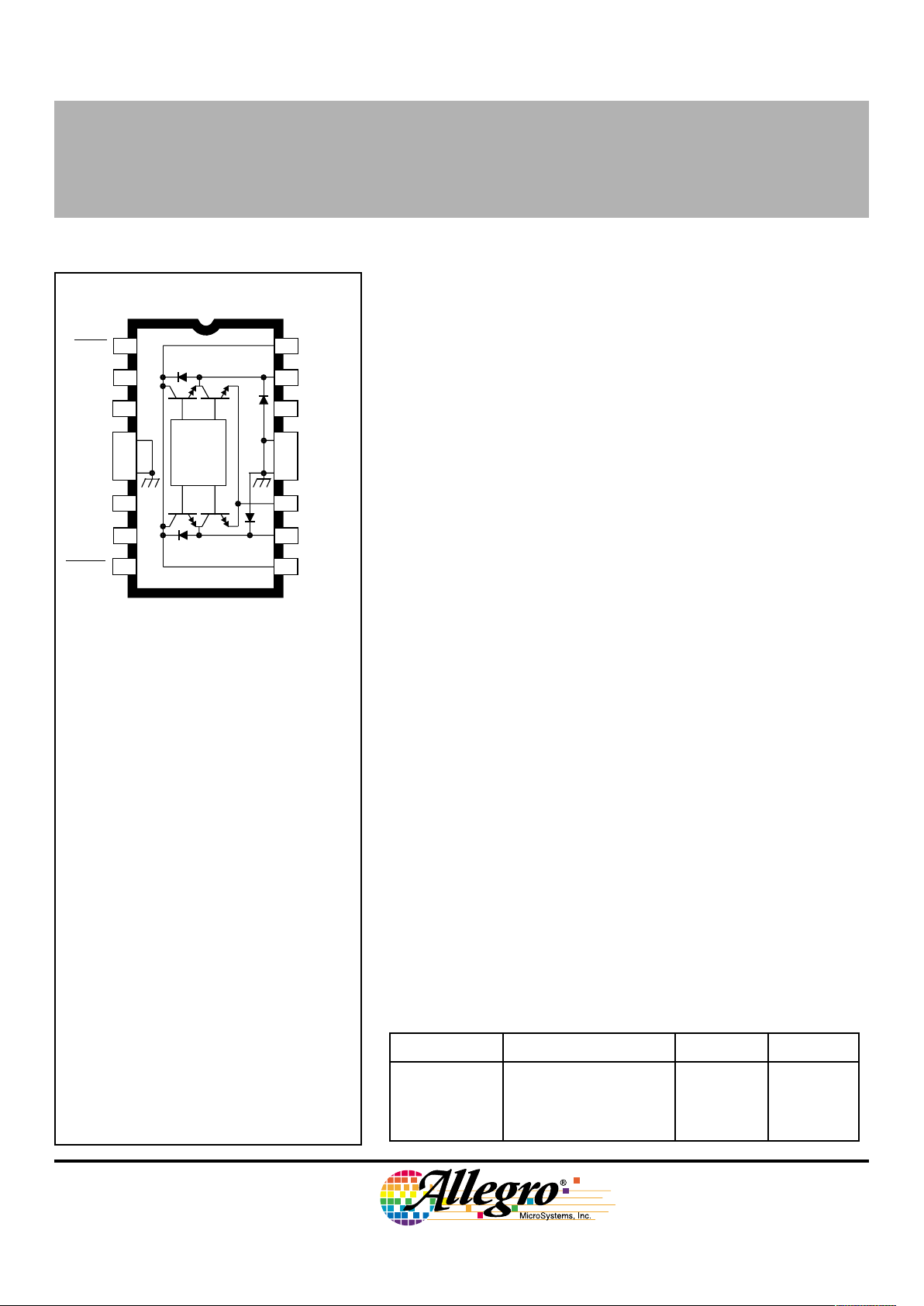
The A3952S– is supplied in a choice of four power packages. In all
package styles, the batwing/power tab is at ground potential and needs
no isolation. These devices are also available for operation from -40°C
to +125°C. To order, change the suffix from 'S–' to 'K–'.
FEATURES
■ ±2 A Continuous Output Current Rating
■ 50 V Output Voltage Rating
■ Internal PWM Current Control
■ Fast and Slow Current-Decay Modes
■ Sleep (Low Current Consumption) Mode
■ Internal Transient Suppression Diodes
■ Under-Voltage Lockout
■ Internal Thermal Shutdown Circuitry
■ Crossover-Current Protection
Always order by complete part number:
Part Number Package R
θJA
R
θJT
A3952SB 16-Pin DIP 43°C/W 6.0°C/W
A3952SEB 28-Lead PLCC 42°C/W 6.0°C/W
A3952SLB 16-Lead SOIC 67°C/W 6.0°C/W
A3952SW 12-Pin Power-Tab SIP 36°C/W 2.0°C/W
A3952SB
Note that the A3952SB (DIP) and the A3952SLB
(SOIC) are electrically identical and share a
common terminal number assignment.
ABSOLUTE MAXIMUM RATINGS
Load Supply Voltage, V
BB
.................. 50 V
Output Current, I
OUT
(t
w
≤ 20 µs).................................. ±3.5 A
(Continuous) ...............................
±2.0 A
Logic Supply Voltage, V
CC
................. 7.0 V
Logic Input Voltage Range,
V
IN
....................... -0.3 V to VCC + 0.3 V
Sense Voltage, V
SENSE
...................... 1.5 V
Reference Voltage, V
REF
.................... 15 V
Package Power Dissipation,
P
D
....................................... See Graph
Operating Temperature Range,
T
A
............................... –20°C to +85°C
Junction Temperature, T
J
............. +150°C*
Storage Temperature Range,
T
S
............................. –55°C to +150°C
Output current rating may be limited by duty cycle,
ambient temperature, heat sinking and/or forced
cooling. Under any set of conditions, do not
exceed the specified current rating or a junction
temperature of +150°C.
* Fault conditions that produce excessive junction
temperature will activate device thermal shutdown
circuitry. These conditions can be tolerated but
should be avoided.
3952
MODE
GROUND
GROUND
LOGIC
SUPPLY
PHASE
GROUND
GROUND
RC
SENSE
LOAD
SUPPLY
Dwg. PP-056
BRAKE
REF
LOAD
SUPPLY
V
CC
OUT
B
OUT
A
V
BB
V
BB
LOGIC
ENABLE
1
2
3
4
5
6
7
89
10
11
12
13
14
15
16
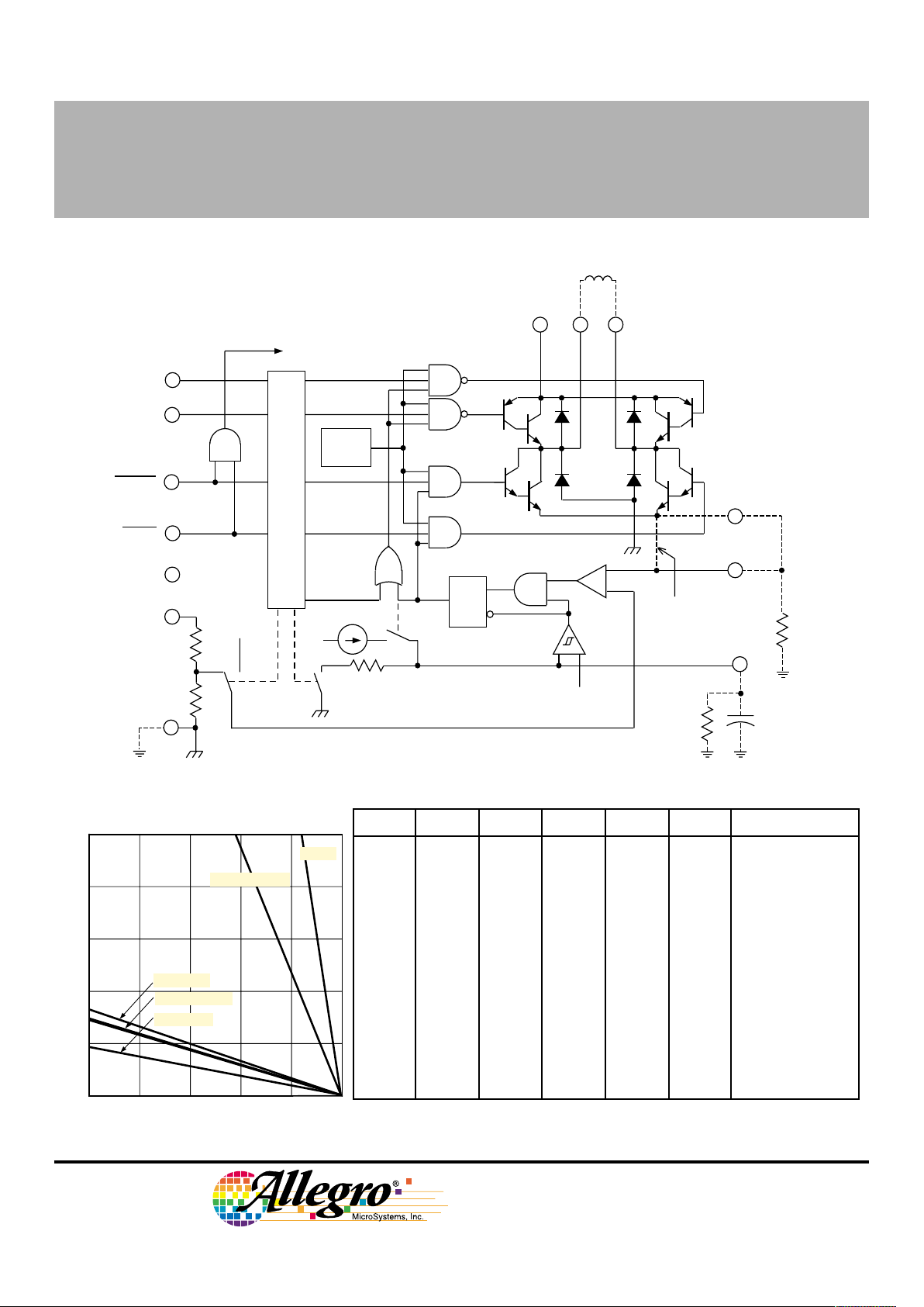
3952
FULL-BRIDGE
PWM MOTOR DRIVER
115 Northeast Cutoff, Box 15036
Worcester, Massachusetts 01615-0036 (508) 853-5000
V
BB
RC
V
CC
LOGIC
SUPPLY
LOAD
SUPPLY
PHASE
EMITTERS
UVLO
& TSD
R
S
Dwg. FP-036
MODE
REF
OUT
A
OUT
B
ENABLE
SENSE
–
+
BRAKE
9R
R
INPUT LOGIC
GROUND
Q
R
S
1.5 V
PWM LATCH
V
CC
+ –
BLANKING
SLEEP &
STANDBY MODES
V
TH
'EB' ONLY
'B', 'LB', & 'W'
PACKAGES
R
T
C
T
FUNCTIONAL BLOCK DIAGRAM
TRUTH TABLE
BRAKE ENABLE PHASE MODE OUT
A
OUTBDESCRIPTION
H H X H Z Z Sleep Mode
H H X L Z Z Standby, Note 1
H L H H H L Forward,
Fast-Decay Mode
H L H L H L Forward,
Slow-Decay Mode
H L L H L H Reverse,
Fast-Decay Mode
H L L L L H Reverse,
Slow-Decay Mode
L X X H L L Brake,
Fast-Decay Mode
L X X L L L Brake, No Current
Control, Note 2
X = Irrelevant Z = High Impedance (source and sink both OFF)
NOTES: 1. Includes active pull-offs for power outputs.
2. Includes internal default V
sense
level for over-current protection.
50 75 100 125 150
10
6
4
2
0
TEMPERATURE IN °C
8
25
Dwg. GP-007-1A
ALLOWABLE PACKAGE POWER DISSIPATION IN WATTS
'W' TAB
'B' , 'EB', & 'LB' TAB
'W' AMBIENT
'B' & 'EB' AMBIENT
'LB' AMBIENT
Copyright © 1994 Allegro MicroSystems, Inc.
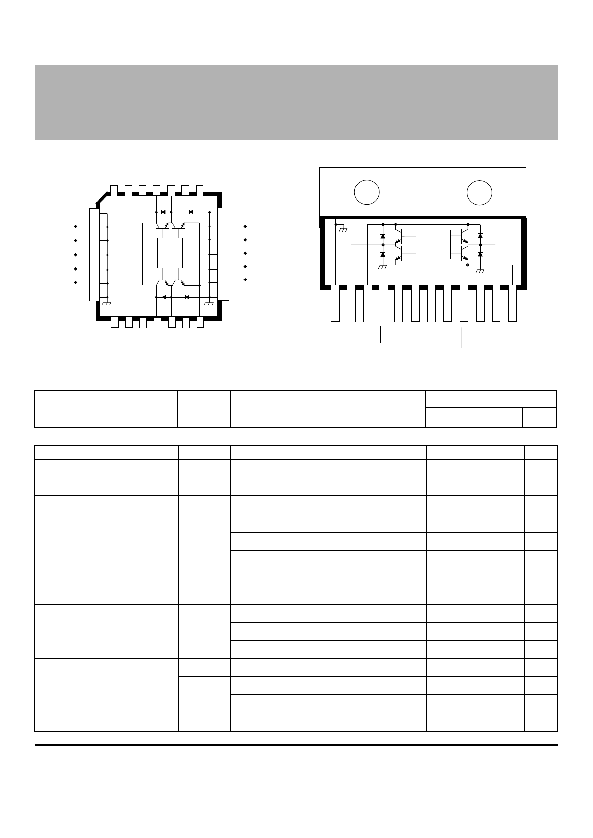
3952
FULL-BRIDGE
PWM MOTOR DRIVER
A3952SEB A3952SW
ELECTRICAL CHARACTERISTICS at T
A
= +25°C, V
BB
= 50 V, VCC = 5.0 V, V
BRAKE
= 2.0 V,
V
SENSE
= 0 V, RC = 20 kΩ/1000 pF to Ground (unless noted otherwise).
Limits
Characteristic Symbol Test Conditions Min. Typ. Max. Units
Output Drivers
Load Supply Voltage Range V
BB
Operating, I
OUT
= ±2.0 A, L = 3 mH V
CC
– 50 V
Output Leakage Current I
CEX
V
OUT
= V
BB
– <1.0 50 µA
V
OUT
= 0 V – <-1.0 -50 µA
Output Saturation Voltage V
CE(SAT)
Source Driver, I
OUT
= -0.5 A – 0.9 1.2 V
Source Driver, I
OUT
= -1.0 A – 1.0 1.4 V
Source Driver, I
OUT
= -2.0 A – 1.2 1.8 V
Sink Driver, I
OUT
= +0.5 A – 0.9 1.2 V
Sink Driver, I
OUT
= +1.0 A – 1.0 1.4 V
Sink Driver, I
OUT
= +2.0 A – 1.3 1.8 V
Clamp Diode Forward Voltage V
F
IF = 0.5 A – 1.0 1.4 V
(Source or Sink) IF = 1.0 A – 1.1 1.6 V
IF = 2.0 A – 1.4 2.0 V
Load Supply Current I
BB(ON)
V
ENABLE
= 0.8 V – 2.9 6.0 mA
(No Load) I
BB(OFF)
V
ENABLE
= 2.0 V, V
MODE
= 0.8 V – 3.1 6.5 mA
V
BRAKE
= 0.8 V – 3.1 6.5 mA
I
BB(SLEEP)
V
ENABLE
= V
MODE
= 2.0 V – <1.0 50 µA
12345 678 9101112
GROUND
Dwg. PP-058
MODE
LOGIC
SUPPLY
PHASE
RC
SENSE
REF
LOAD
SUPPLY
OUT
B
OUT
A
ENABLE
V
CC
V
BB
LOGIC
BRAKE
1
2
3
4
5
6
7
8
9
10
11
12
13
14
15
16
17
18
19
20
21
22
23
24
25
26
27
28
GROUND
GROUND
GROUND
GROUND
Dwg. PP-057
NOCONNECTION
EMITTERS
RC
LOAD
SUPPLY
REF
V
CC
V
BB
LOGIC
BRAKE
LOGIC
SUPPLY
PHASE
ENABLE
MODE
SENSE
LOAD
SUPPLY
OUT
B
OUT
A
Continued next page …

3952
FULL-BRIDGE
PWM MOTOR DRIVER
115 Northeast Cutoff, Box 15036
Worcester, Massachusetts 01615-0036 (508) 853-5000
Control Logic
Logic Supply Voltage Range V
CC
Operating 4.5 5.0 5.5 V
Logic Input Voltage V
IN(1)
2.0 ––V
V
IN(0)
––0.8 V
Logic Input Current I
IN(1)
VIN = 2.0 V – <1.0 20 µA
I
IN(0)
VIN = 0.8 V – <-2.0 -200 µA
Reference Voltage Range V
REF
Operating 0 – 15 V
Reference Input Current I
REF
V
REF
= 2.0 V 25 40 55 µA
Reference Voltage Divider Ratio – V
REF
= 15 V 9.5 10.0 10.5 –
Comparator Input Offset Voltage V
IO
V
REF
= 0 V – ±1.0 ±10 mV
PWM RC Fixed OFF Time t
off
CT = 1000 pF, RT = 20 kΩ 18 20 22 µs
PWM Minimum ON Time t
on(min)
CT = 820 pF, RT ≥ 12 kΩ – 1.7 3.0 µs
CT = 1200 pF, RT ≥ 12 kΩ – 2.5 3.8 µs
Propagation Delay Time t
pd
I
OUT
= ±2.0 A, 50% EIN to 90% E
OUT
Transition:
ENABLE ON to Source ON – 2.9 – µs
ENABLE OFF to Source OFF – 0.7 – µs
ENABLE ON to Sink ON – 2.4 – µs
ENABLE OFF to Sink OFF – 0.7 – µs
PHASE Change to Source ON – 2.9 – µs
PHASE Change to Source OFF – 0.7 – µs
PHASE Change to Sink ON – 2.4 – µs
PHASE Change to Sink OFF – 0.7 – µs
t
pd(pwm)
Comparator Trip to Sink OFF – 0.8 1.5 µs
Thermal Shutdown Temperature T
J
– 165 – °C
Thermal Shutdown Hysteresis ∆T
J
– 15 – °C
UVLO Disable Threshold V
CC(UVLO)
3.15 3.50 3.85 V
UVLO Hysteresis ∆V
CC(UVLO)
300 400 500 mV
Logic Supply Current I
CC(ON)
V
ENABLE
= 0.8 V, V
BRAKE
= 2.0 V – 20 30 mA
(No Load) I
CC(OFF)
V
ENABLE
= 2.0 V, V
MODE
= 0.8 V – 12 18 mA
I
CC(BRAKE)
V
BRAKE
= 0.8 V – 26 40 mA
I
CC(SLEEP)
V
ENABLE
= V
MODE
= V
BRAKE
= 2.0 V – 3.0 5.0 mA
NOTES: 1. Typical Data is for design information only.
2. Each driver is tested separately.
3. Negative current is defined as coming out of (sourcing) the specified device terminal.
Limits
Characteristic Symbol Test Conditions Min. Typ. Max. Units
3952
FULL-BRIDGE
PWM MOTOR DRIVER
FUNCTIONAL DESCRIPTION
INTERNAL PWM CURRENT CONTROL DURING
FORWARD AND REVERSE OPERATION
The A3952S– contains a fixed OFF-time pulse-width
modulated (PWM) current-control circuit that can be used
to limit the load current to a desired value. The value of
the current limiting (I
TRIP
) is set by the selection of an
external current sensing resistor (RS) and reference input
voltage (V
REF
). The internal circuitry compares the voltage
across the external sense resistor to one tenth the voltage
on the REF input terminal, resulting in a function approximated by
I
TRIP
= V
REF
/(10RS).
In forward or reverse mode the current-control circuitry
limits the load current. When the load current reaches
I
TRIP
, the comparator resets a latch to turn OFF the
selected sink driver (in the slow-decay mode) or selected
sink and source driver pair (in the fast-decay mode). In
slow-decay mode, the selected sink driver is disabled; the
load inductance causes the current to recirculate through
the source driver and flyback diode (see figure 1). In fastdecay mode, the selected sink and source driver pair are
disabled; the load inductance causes the current to flow
from ground to the load supply via the ground clamp and
flyback diodes.
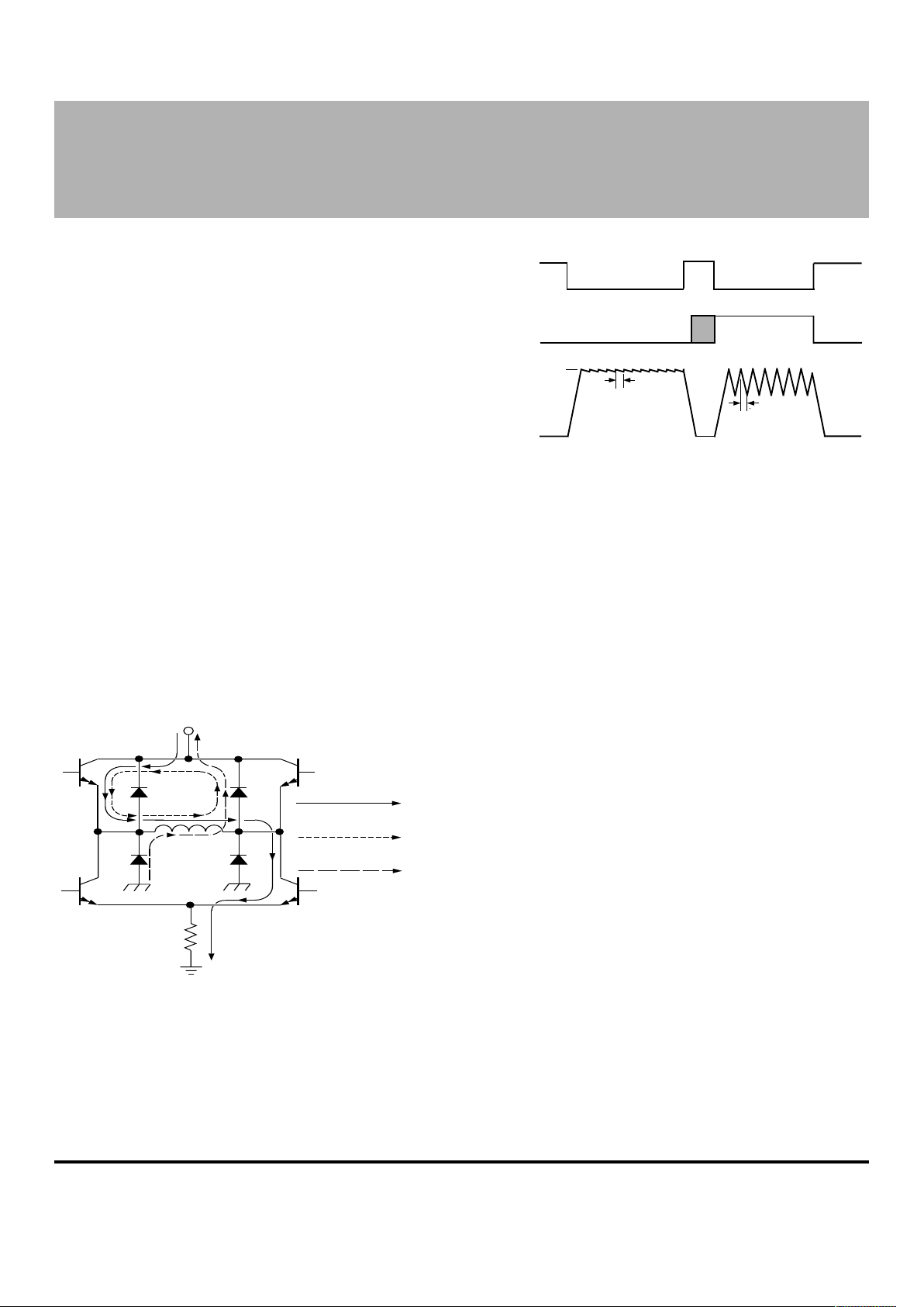
Figure 1 — Load-Current Paths
The user selects an external resistor (RT) and capacitor (CT) to determine the time period (t
off
= RTCT) during
which the drivers remain disabled (see “RC Fixed OFF
Time” below). At the end of the RTCT interval, the drivers
are re-enabled allowing the load current to increase again.
The PWM cycle repeats, maintaining the load current at
the desired value (see figure 2).
ENABLE
MODE
LOAD
CURRENT
RC
I
TRIP
Dwg. WP-015-1
RC
Dwg. EP-006-2A
R
S
BB
V
DRIVE CURRENT
RECIRCULATION
(SLOW-DECAY MODE)
RECIRCULATION
(FAST-DECAY MODE)
Figure 2 — Fast and Slow Current-Decay Waveforms
INTERNAL PWM CURRENT CONTROL DURING
BRAKE MODE OPERATION
The brake circuit turns OFF both source drivers and
turns ON both sink drivers. For dc motor applications, this
has the effect of shorting the motor’s back-EMF voltage,
resulting in current flow that brakes the motor dynamically.
However, if the back-EMF voltage is large, and there is no
PWM current limiting, then the load current can increase to
a value that approaches a locked rotor condition. To limit
the current, when the I
TRIP
level is reached, the PWM
circuit disables the conducting sink driver. The energy
stored in the motor’s inductance is then discharged into
the load supply causing the motor current to decay.
As in the case of forward/reverse operation, the drivers
are re-enabled after a time given by t
off
= RTCT (see “RC
Fixed OFF Time” below). Depending on the back-EMF
voltage (proportional to the motor’s decreasing speed), the
load current again may increase to I
TRIP
. If so, the PWM
cycle will repeat, limiting the load current to the desired
value.
Brake Operation - MODE Input High
During braking, when the MODE input is high, the
current limit can be approximated by
I
TRIP
= V
REF
/(10RS).
CAUTION: Because the kinetic energy stored in the
motor and load inertia is being converted into current,
which charges the VBB supply bulk capacitance (power
supply output and decoupling capacitance), care must be
taken to ensure the capacitance is sufficient to absorb the
energy without exceeding the voltage rating of any devices
connected to the motor supply.
 Loading...