

Allegro A3951SW, A3951SB Datasheet
29319.4†
3951
FULL-BRIDGE PWM MOTOR DRIVER
Data Sheet
A3951SB
LOAD
1
REF/
BRAKE
GROUND
GROUND
LOGIC
SUPPLY
PHASE
ENABLE
NC
RC
2
3
4
5
6
V
CC
7
8
LOGIC
V
BB
V
BB
ABSOLUTE MAXIMUM RATINGS
Load Supply Voltage, V
Output Current, I
(tw ≤ 20 µs) .................................. ±3.5 A
(Continuous) ............................... ±2.0 A
Logic Supply Voltage, VCC.................. 7.0 V
Logic Input Voltage Range,
........................ -0.3 V to VCC + 0.3 V
V
IN
Sense Voltage, V
Reference Voltage, V
Package Power Dissipation,
PD ....................................... See Graph
Operating Temperature Range,
............................... –20°C to +85°C
T
A
Junction Temperature, TJ ............. +150°C*
Storage Temperature Range,
TS ............................. –55°C to +150°C
Output current rating may be limited by duty cycle,
ambient temperature, heat sinking and/or forced
cooling. Under any set of conditions, do not
exceed the specified current rating or a junction
temperature of +150°C.
* Fault conditions that produce excessive junction
temperature will activate device thermal shutdown
circuitry. These conditions can be tolerated but
should be avoided.
BB
OUT
........................ 1.5 V
SENSE
....................... V
REF
16
SUPPLY
15
OUT
B
14
GROUND
13
GROUND
12
GROUND
11
SENSE
10
OUT
A
LOAD
9
SUPPLY
Dwg. PP-056-1
................... 50 V
CC
Designed for bidirectional pulse-width modulated current control of
inductive loads, the A3951SB and A3951SW are capable of continuous
output currents to ±2 A and operating voltages to 50 V. Internal fixed
off-time PWM current-control circuitry can be used to regulate the
maximum load current to a desired value. The peak load current limit is
set by the user’s selection of an input reference voltage and external
sensing resistor. The fixed off-time pulse duration is set by a userselected external RC timing network. Internal circuit protection includes
thermal shutdown with hysteresis, transient suppression diodes, and
crossover-current protection. Special power-up sequencing is not
required. The A3951SB and A3951SW are improved replacements for
the UDN2953B and UDN2954W, respectively. For new system designs, the A3952SB/SEB/SLB/SW are recommended.
With the ENABLE input held low, the PHASE input controls load
current polarity by selecting the appropriate source and sink driver pair.
A user-selectable blanking window prevents false triggering of the PWM
current control circuitry. With the ENABLE input held high, all output
drivers are disabled.
When a logic low is applied to the BRAKE input, the braking
function is enabled. This overrides ENABLE and PHASE to turn off
both source drivers and turn on both sink drivers. The brake function
can be safely used to dynamically brake brush dc motors.
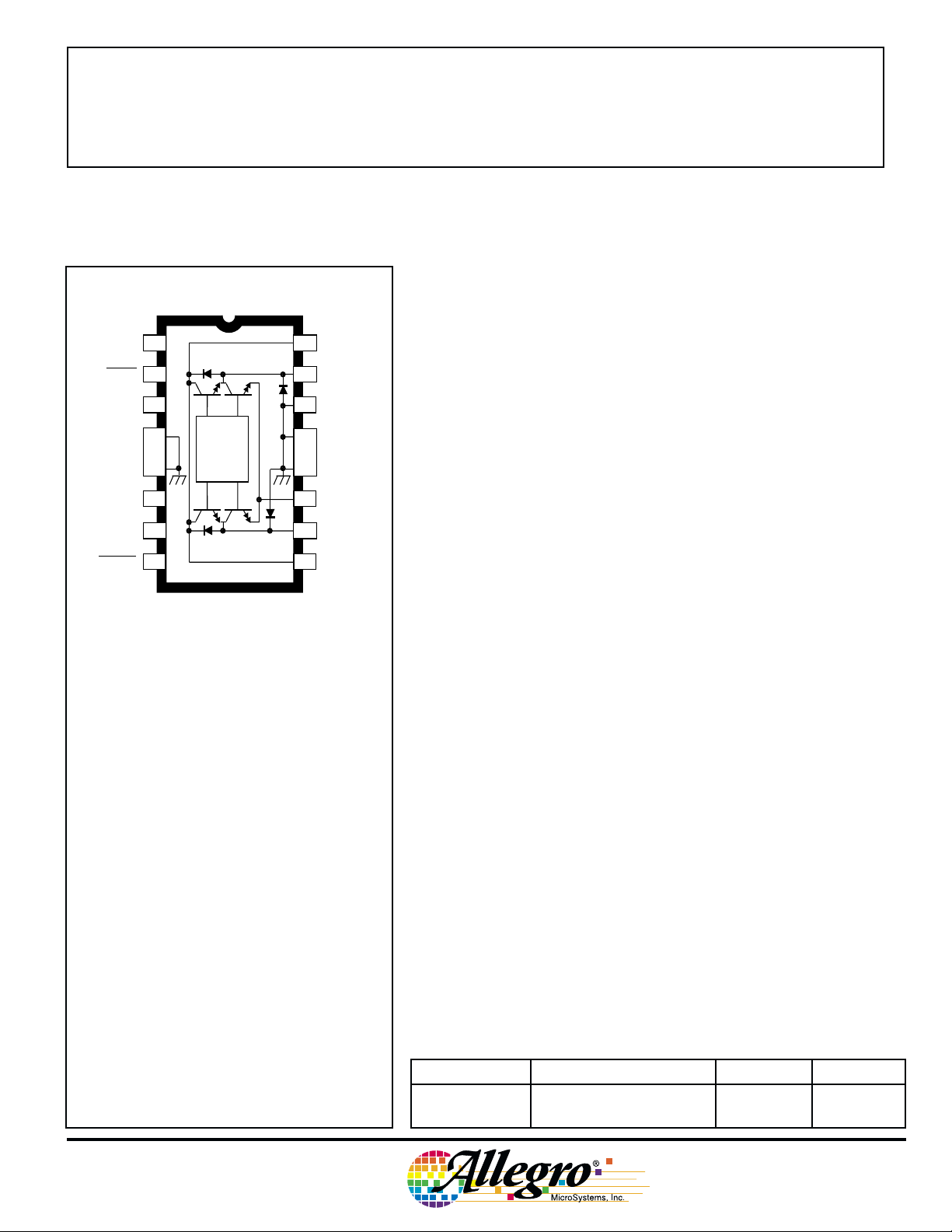
The A3951SB is supplied in a 16-pin dual in-line plastic package
with copper heat-sink contact tabs. The lead configuration enables
easy attachment of a heat sink while fitting a standard printed wiring
board layout. The A3951SW, for higher package power dissipation
requirements, is supplied in a 12-pin single in-line power-tab package.
In either package style, the batwing/power tab is at ground potential
and needs no isolation.
FEATURES
■ ±2 A Continuous Output Current Rating
■ 50 V Output Voltage Rating
■ Internal PWM Current Control
■ Internal Transient Suppression Diodes
■ Under-Voltage Lockout
■ Internal Thermal Shutdown Circuitry
■ Crossover-Current Protection
■ Default Brake Current Limit
Always order by complete part number:
Part Number Package R
θJA
A3951SB 16-Pin DIP 43°C/W 6.0°C/W
A3951SW 12-Pin Power-Tab SIP 36°C/W 2.0°C/W
R
θJT
3951
FULL-BRIDGE
PWM MOTOR DRIVER
FUNCTIONAL BLOCK DIAGRAM
ENABLE
REF/
GROUND
PHASE
BRAKE
9R
A
LOGIC
SUPPLY
CC
V
UVLO
& TSD
INPUT LOGIC
R
Q
1.5 V
R
BLANKING
V
CC
S
PWM LATCH
LOAD
SUPPLY
BB
V
+ –
OUT
V
TH
B
OUT
+
–
SENSE
RC
R
S
10
SUFFIX 'W',
R = 2.0°C/W
θJT
8
SUFFIX 'B',
R = 6.0°C/W
θJT
6
4
SUFFIX 'W', R = 38°C/W
2
SUFFIX 'B', R = 43°C/W
0
ALLOWABLE PACKAGE POWER DISSIPATION IN WATTS
25
θJA
50 75 100 125 150
TEMPERATURE IN °C
θJA
2
TRUTH TABLE
BRAKE ENABLE PHASE OUT
H H X Z Z Outputs Disabled
H L H H L Forward
H L L L H Reverse
L X X L L Brake, See Note
X = Irrelevant Z = High Impedance (source and sink both off)
NOTE: Includes internal default V
Dwg. GP-032A
115 Northeast Cutoff, Box 15036
Worcester, Massachusetts 01615-0036 (508) 853-5000
Copyright © 1994, 2000 Allegro MicroSystems, Inc.
OUTBDESCRIPTION
A
level for over-current protection.
sense
Dwg. FP-036-1
PWM MOTOR DRIVER
A3951SW
LOGIC
BB
V
CC
V
1 2 3 4 5 6 7 8 9 10 11 12
OUT
GROUND
B
LOAD
LOAD
SUPPLY
SUPPLY
BRAKE
REF/
RC
LOGIC
PHASE
SUPPLY
ENABLE
A
OUT
NC
Dwg. PP-058-1
3951
FULL-BRIDGE
SENSE
ELECTRICAL CHARACTERISTICS at TA = +25°C, VBB = 50 V, VCC = 5.0 V,
V
= 2.0 V, V
REF
Characteristic Symbol Test Conditions Min. Typ. Max. Units
Output Drivers
Load Supply Voltage Range V
Output Leakage Current I
Output Saturation Voltage V
Clamp Diode Forward Voltage V
(Source or Sink) IF = 1.0 A – 1.1 1.6 V
= 0 V, RC = 20 kΩ/1000 pF to Ground (unless noted otherwise).
SENSE
BB
CEX
CE(SAT)
F
Operating, I
V
= V
OUT
V
= 0 V – <-1.0 -50 µA
OUT
Source driver, I
Source driver, I
Source driver, I
Sink driver, I
Sink driver, I
Sink driver, I
IF = 0.5 A – 1.0 1.4 V
= ±2.0 A, L = 3 mH V
OUT
BB
= -0.5 A – 0.9 1.2 V
OUT
= -1.0 A – 1.0 1.4 V
OUT
= -2.0 A – 1.2 1.8 V
OUT
= +0.5 A – 0.9 1.2 V
OUT
= +1.0 A – 1.0 1.4 V
OUT
= +2.0 A – 1.3 1.8 V
OUT
Limits
CC
– 50 V
– <1.0 50 µA
Load Supply Current I
(No Load) I
I
www.allegromicro.com
BB(ON)
BB(OFF)
BB(BRAKE)
IF = 2.0 A – 1.4 2.0 V
V
V
V
= 0.8 V, V
ENABLE
= V
ENABLE
BRAKE
REF
= 0.8 V – 3.1 6.5 mA
= 2.0 V – 2.9 6.0 mA
REF
= 2.0 V – 3.1 6.5 mA
Continued next page …
3

3951
FULL-BRIDGE
PWM MOTOR DRIVER
ELECTRICAL CHARACTERISTICS (Continued)
Limits
Characteristic Symbol Test Conditions Min. Typ. Max. Units
Control Logic
Logic Supply Voltage Range V
Logic Input Voltage V
Logic Input Current I
Reference Voltage Range V
Reference Input Current I
V
IN(1)
I
IN(0)
REF
CC
IN(1)
IN(0)
REF
Reference Voltage Divider Ratio – V
PWM RC Fixed Off Time t
PWM Minimum On Time t
Propagation Delay Time t
off
on(min)
pd
Operating 4.5 5.0 5.5 V
2.0 ––V
––0.8 V
VIN = 2.0 V – <1.0 20 µA
VIN = 0.8 V – <-2.0 -200 µA
Operating 2.0 – V
2.0 V ≤ V
= 5 V 9.5 10.0 10.5 –
REF
REF
≤ V
CC
25 40 55 µA
CC
V
CT = 1000 pF, RT = 20 kΩ 18 20 22 µs
CT = 820 pF, RT ≥ 12 kΩ – 1.7 3.0 µs
CT = 1200 pF, RT ≥ 12 kΩ – 2.5 3.8 µs
I
= ±2.0 A, 50% EIN to 90% E
OUT
transition:
OUT
ENABLE on to source driver on – 2.9 – µs
ENABLE off to source driver off – 0.7 – µs
ENABLE on to sink driver on – 2.4 – µs
ENABLE off to sink driver off – 0.7 – µs
PHASE change to source driver on – 2.9 – µs
t
pd(pwm)
Thermal Shutdown Temperature T
Thermal Shutdown Hysteresis ∆T
UVLO Disable Threshold V
UVLO Hysteresis ∆V
Logic Supply Current I
(No Load) I
J
J
CC(UVLO)
CC(UVLO)
CC(ON)
CC(OFF)
I
CC(BRAKE)
NOTES: 1. Typical Data is for design information only.
2. Each driver is tested separately.
3. Negative current is defined as coming out of (sourcing) the specified device terminal.
4
PHASE change to source driver off – 0.7 – µs
PHASE change to sink driver on – 2.4 – µs
PHASE change to sink driver off – 0.7 – µs
Comparator trip to sink driver off – 0.8 1.5 µs
– 165 – °C
– 15 – °C
3.15 3.50 3.85 V
300 400 500 mV
V
V
V
= 0.8 V, V
ENABLE
= V
ENABLE
REF
115 Northeast Cutoff, Box 15036
Worcester, Massachusetts 01615-0036 (508) 853-5000
REF
= 0.8 V – 26 40 mA
= 2.0 V – 20 30 mA
REF
= 2.0 V – 12 18 mA
 Loading...