

查询A3950供应商查询A3950供应商
Preliminary Data Sheet
Subject to Change without Notice
November 4, 2005
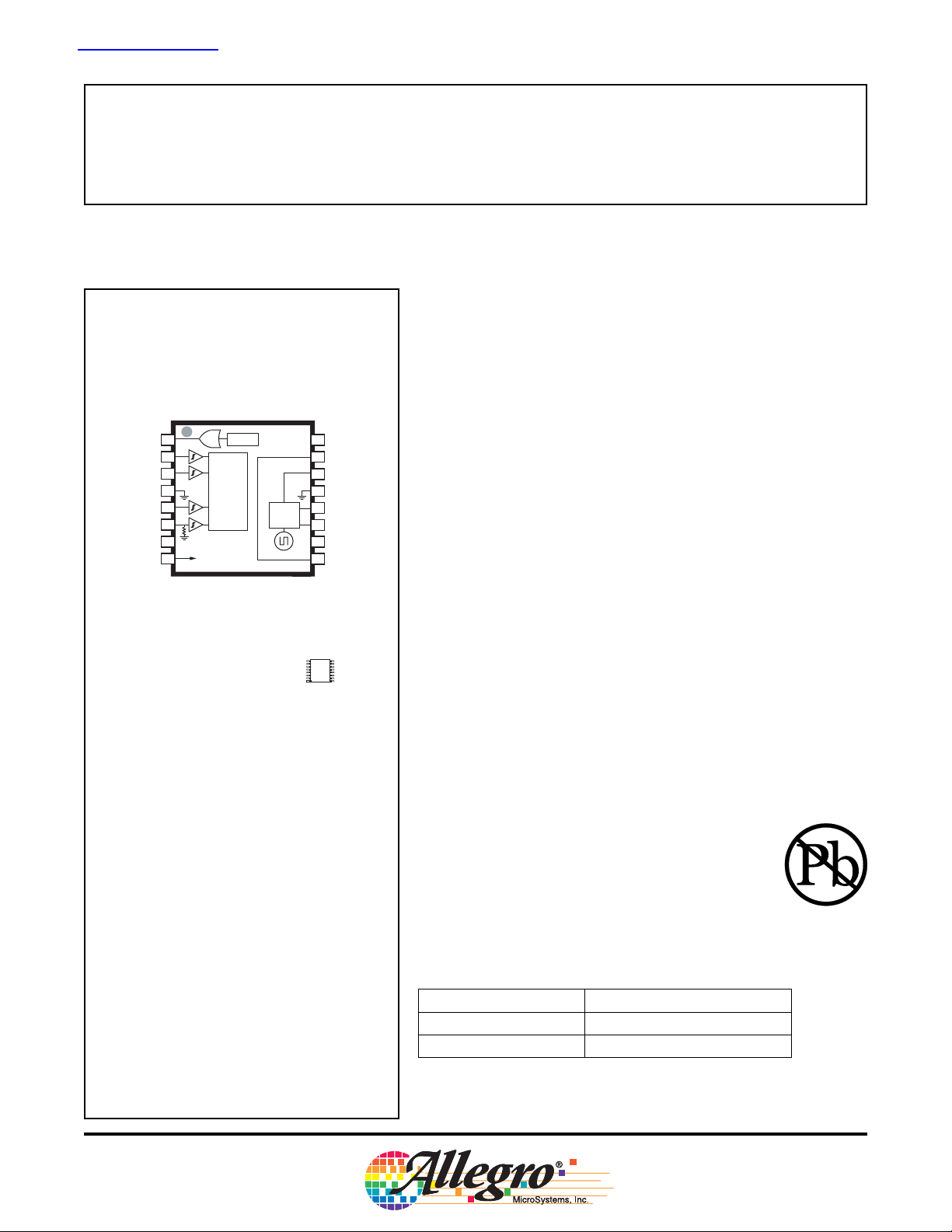
Package LP, 16-pin TSSOP
with Exposed Thermal Pad
Control
Logic
Fault
Charge
Pump
NFAULT
MODE
PHASE
GND
SLEEP
ENABL
OUTA
SENSE
1
2
3
4
5
6
7
8
A3950
DMOS Full-Bridge Motor Driver
Designed for PWM (pulse width modulated) control of dc motors, the
A3950 is capable of peak output currents to ±2.8 A and operating voltages to 36 V.
PHASE and ENABLE input terminals are provided for use in controlling the speed and direction of a dc motor with externally applied PWM
control signals. Internal synchronous rectification control circuitry is
provided to lower power dissipation during PWM operation.
16
NC
15
VREG
14
VCP
13
GND
12
CP2
11
CP1
10
OUTB
9
VBB
Internal circuit protection includes motor lead short-to-supply / short-toground, thermal shutdown with hysteresis, undervoltage monitoring of
VBB and VCP, and crossover-current protection.
The A3950 is supplied in a thin profile (<1.2 mm overall height) 16-pin
TSSOP package with exposed thermal pad (package LP). It is lead (Pb)
free with 100% matte tin leadframe plating.
Approximate Scale 1:1
AB SO LUTE MAX I MUM RAT INGS
Load Supply Voltage, V
Output Current, I
Sense Voltage, V
BB.............................................
OUT.......................................................
.................................±500 mV
SENSE
VBB to OUTx.................................................... 36 V
OUTx to SENSE ................................................ 36 V
Logic Input Voltage, V
..........................–0.3 to 7 V
IN
Operating Temperature Range
Ambient, T
Junction Temperature, T
Storage Temperature, T
, Range S .................... –20°C to 85°C
A
............................ 150°C
J(MAX)
................. –40°C to 125°C
S
36 V
2.8 A
FEATURES
Low R
Overcurrent protection
Motor lead short-to-supply protection
Short-to-ground protection
Sleep function
Synchronous rectification
Diagnostic output
Internal UVLO
Crossover-current protection
Use the following complete part numbers when ordering:
Part Number Packing
A3950SLP-T 96 pieces / tube
A3950SLPTR-T 13-in. reel, 4000 pieces / reel
DS(on)
outputs
A3950DS
Preliminary Data Sheet
Subject to Change without Notice
November 4, 2005
DMOS Full-Bridge Motor Driver
Functional Block Diagram
0.1 µF
CP2
CP1
A3950
VREG
22 µF
25 V
MODE
PHASE
ENABLE
SLEEP
NFAULT
Charge
Pump
Low-Side
Gate Supply
Bias
Supply
Control Logic
UVLO
STB
STG
TSD Warning
GND GND
Pad
Motor Lead
Protection
VBB
OUTA
OUTB
SENSE
VCP
VBB
0.1 µF
OUTA
OUTB
SENSE
0.1 µF
Load Supply
R
SENSE
100 µF
Control Logic Table
PHASE ENABLE MODE SLEEP OUTA OUTB
1
Pin
Function
1 1 X 1 H L Forward
0 1 X 1 L H Reverse
X 0 1 1 L L Brake (slow decay)
1001LHFast Decay Synchronous Rectification
0001HLFast Decay Synchronous Rectification
XXX0ZZ
1X iindicates “don’t care,” Z indicates high impedence.
2To prevent reversal of current during fast decay synchronous rectification, outputs go to the high impedance state as the current approaches 0 A.
A3950DS
Sleep Mode
Allegro MicroSystems, Inc.
115 Northeast Cutoff, Box 15036
Worcester, Massachusetts 01615-0036 (508) 853-5000
www.allegromicro.com
2
2
2
Preliminary Data Sheet
Subject to Change without Notice
November 4, 2005
DMOS Full-Bridge Motor Driver
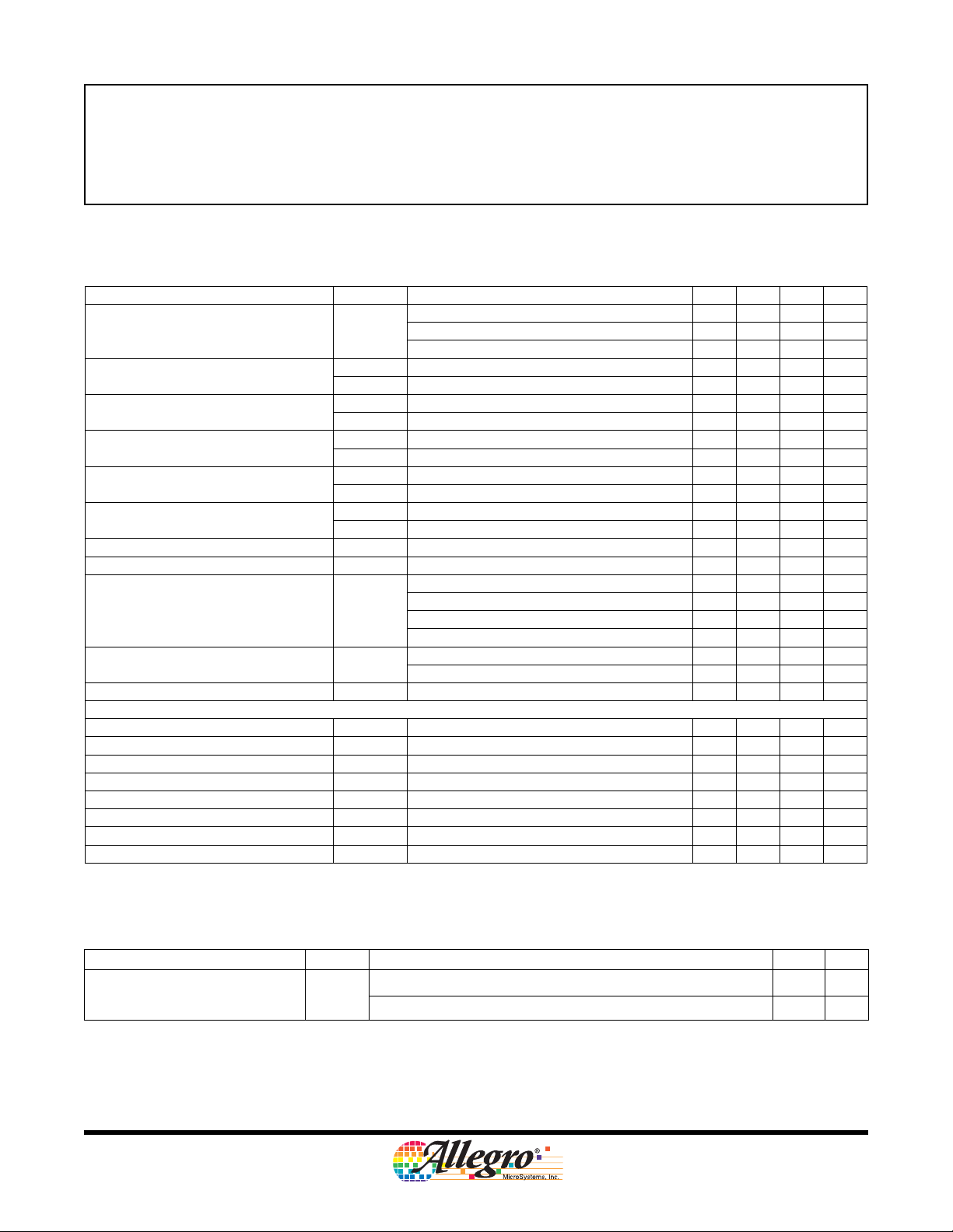
ELECTRICAL CHARACTERISTICS at TJ = 25°C, VBB = 8 to 36 V, unless noted otherwise
Characteristics Symbol Test Conditions Min. Typ. Max. Units
f
< 50 kHz – 6 8.5 mA
Motor Supply Current I
PHASE, ENABLE, MODE Input
Voltage
SLEEP Input Voltage
PHASE, MODE Input Current
1
ENABLE Input Current
SLEEP Input Current
BB
V
V
V
V
I
I
I
I
I
I
NFAULT Output Voltage V
Input Hysteresis, except SLEEP V
Output On Resistance R
IHys
DS(on)
Propagation Delay Time t
Crossover Delay t
COD
Protection Circuitry
UVLO Threshold V
UVLO Hysteresis V
Overcurrent Threshold
2
Overcurrent Protection Period t
UVHys
I
OCP
OCP
Thermal Warning Temperature T
Thermal Warning Hysteresis T
Thermal Shutdown Temperature T
Thermal Shutdown Hysteresis T
1
For input and output current specifications, negative current is defined as coming out of (sourcing) the specified device pin.
2
Overcurrent protection is tested at 25°C in a restricted range and guaranteed by characterization.
JWHys
JTSD
JTSDHys
PWM
Charge pump on, outputs disabled – 3 4.5 mA
Sleep mode – – 10 μA
IH
IL
IH
IL
VIN = 2.0 V – <1.0 20 μA
IH
V
IL
IH
IL
IH
IL
OL
= 0.8 V – <–2.0 –20 μA
IN
VIN = 2.0 V – 40 100 μA
VIN = 0.8 V – 16 40 μA
VIN = 2.7 V – 27 50 μA
VIN = 0.8 V – <1 10 μA
I
= 1.0 mA – – 0.4 V
sink
2.0 – – V
– – 0.8 V
2.7 – – V
– – 0.8 V
100 150 200 mV
Source driver, I
Source driver, I
Sink driver, I
Sink driver, I
= -2.8 A, TJ=25°C – 0.35 0.48 Ω
OUT
= -2.8 A, TJ=125°C – 0.55 0.8 Ω
OUT
= 2.8 A, TJ=25°C – 0.3 0.43 Ω
OUT
= 2.8 A, TJ=125°C – 0.45 0.7 Ω
OUT
PWM, change to source or sink ON – 600 – ns
pd
PWM, change to source or sink OFF – 100 – ns
– 500 – ns
VBB increasing – 6.5 – V
UV
– 250 – mV
3––A
– 1.2 – ms
Temperature increasing – 160 – °C
JW
Recovery = TJW – T
JWHys
–15–°C
Temperature increasing – 175 – °C
Recovery = T
JTSD
– T
JTSDHys
–15–°C
A3950
THERMAL CHARACTERISTICS may require derating at maximum conditions, see application information
Characteristic Symbol Test Conditions* Value Units
Package Thermal Resistance R
*Additional thermal data available on the Allegro Web site.
A3950DS
4-layer PCB based on JEDEC standard 34 ºC/W
θJA
2-layer PCB with 3.8 in.
2
copper both sides, connected by thermal vias 43 ºC/W
Allegro MicroSystems, Inc.
115 Northeast Cutoff, Box 15036
Worcester, Massachusetts 01615-0036 (508) 853-5000
www.allegromicro.com
3

Preliminary Data Sheet
Subject to Change without Notice
November 4, 2005
SLEEP
ENABLE
PHASE
MODE
V
BB
V
OUTA
0
A3950
DMOS Full-Bridge Motor Driver
Timing Diagram: PWM Control
V
OUTB
I
OUTX
V
BB
0
0
A 1 2 3 4 5 6 7 98
V
BB
1
5
234
V
BB
6
7
OutBOutAOutA OutB
8
9
A3950DS
A
Charge pump and VREG power-on delay (≈200 µs)
Allegro MicroSystems, Inc.
115 Northeast Cutoff, Box 15036
Worcester, Massachusetts 01615-0036 (508) 853-5000
www.allegromicro.com
4

Preliminary Data Sheet
Subject to Change without Notice
November 4, 2005
Timing Diagram: Overcurrent Control
V
OUTA
High-Z
V
OUTB
A3950
DMOS Full-Bridge Motor Driver
I
OUTx
ENABLE,
Source
or Sink
BLANK
Charge Pump
Counter
NFAULT
I
PEAK
I
OCP
t
BLANK
Motor lead
short condition
t
OCP
Normal dc
motor capacitance
A3950DS
Allegro MicroSystems, Inc.
115 Northeast Cutoff, Box 15036
Worcester, Massachusetts 01615-0036 (508) 853-5000
www.allegromicro.com
5

Preliminary Data Sheet
Subject to Change without Notice
November 4, 2005
A3950
DMOS Full-Bridge Motor Driver
Functional Description
VREG. This supply voltage is used to run the sink-side
DMOS outputs. VREG is internally monitored and in the
case of a fault condition, the outputs of the device are disabled. The VREG pin should be decoupled with a 0.22 μF
capacitor to ground.
Charge Pump. The charge pump is used to generate a
supply above VBB to drive the source-side DMOS gates. A
0.1 μF ceramic monolithic capacitor should be connected
between CP1 and CP2 for pumping purposes. A 0.1 μF
ceramic monolithic capacitor should be connected between
VCP and VBB to act as a reservoir to run the high-side
DMOS devices. The VCP voltage level is internally monitored and, in the case of a fault condition, the outputs of the
device are disabled.
Shutdown. In the event of a fault due to excessive junction
temperature, or low voltage on VCP or VREG, the outputs of
the device are disabled until the fault condition is removed.
At power-on the UVLO circuit disables the drivers.
Sleep Mode. Control input SLEEP is used to minimize
power consumption when the A3950 not in use. This disables
much of the internal circuitry, including the regulator and
charge pump. A logic low setting puts the device into Sleep
mode, and a logic high setting allows normal operation. After
coming out of Sleep mode, provide a 1 ms interval before
applying PWM signals, to to allow the charge pump to
stabilize.
applying an enable chop command. Because it is possible to
drive current in both directions through the DMOS switches,
this configuration effectively shorts out the motor generated
BEMF as long as the ENABLE chop mode is asserted. The
maximum current can be approximated by V
BEMF/RL
. Care
should be taken to insure that the maximum ratings of the
device are not exceeded in worse case braking situations:
high speed and high-inertia loads.
Overcurrent Protection. The voltage on the output pins
relative to supply are monitored to ensure that the motor lead
is not shorted to supply or ground. If a short is detected, the
full-bridge outputs are turned off, flag NFAULT is driven
low, and a 1.2 ms fault timer is started.
After this 1.2 ms period, t
, the device will then be
OCP
allowed to follow the input commands and another turn-on is
attempted. If there is still a fault condition, the cycle repeats.
If, after t
expires, it is determined that the short condi-
OCP
tion is not present, the NFAULT pin is released and normal
operation resumes.
Diagnostic Output. The NFAULT pin signals a problem
with the chip via an open drain output. A motor fault, undervoltage condition, or TJ > 160°C will drive the pin active
low. This output is not valid when SLEEP puts the device
into minimum power dissipation mode.
MODE. Control input MODE is used to toggle between
fast decay mode and slow decay mode. A logic high puts
the device in slow decay mode. Synchronus rectification is
always enabled.
Braking. The braking function is implemented by driving
the device in slow decay mode via the MODE setting and
A3950DS
TSD. Two die temperature monitors are integrated on the
chip. As die temperature increases towards the maximum, a
thermal warning signal will be triggered at 160°C. This fault
drives the NFAULT low, but does not disable the operation of
the chip. If the die temperature increases further, to approximately 175°C, the full-bridge outputs will be disabled until
the internal temperature falls below a hysteresis of 15°C.
Allegro MicroSystems, Inc.
115 Northeast Cutoff, Box 15036
Worcester, Massachusetts 01615-0036 (508) 853-5000
www.allegromicro.com
6

P
Preliminary Data Sheet
Subject to Change without Notice
November 4, 2005
A3950
DMOS Full-Bridge Motor Driver
Applications Information
Power Dissipation. First order approximation of power
dissipation in the A3950 can be calculated by first examining
the power dissipation in the full-bridge during each of the
operation modes. The A3950 features synchronous rectification, a feature that effectively shorts out the body diode by
turning on the low R
DMOS driver during the decay
DS(on)
cycle. This significantly reduces power dissipation in the
full-bridge. In order to prevent shoot-through, where both
source and sink driver are on at the same time, the A3950
implements a 500 ns typical crossover delay time. For this
period, the body diode in the decay current path conducts
the current until the DMOS driver turns on. This does affect
VBB
1
3
2
1
Drive current
Fast decay with synchronous rectification (reverse)
2
Slow decay with synchronous rectification (brake)
3
Figure 1. Current Decay Patterns
power dissipation and may need to be considered in high
current, high ambient temperature applications. In addition,
motor parameters and switching losses can add power dissipation that could affect critical applications.
Drive Current. This current path is through source DMOS
driver, motor winding, and sink DMOS driver. Power dissipation is I2R loses in one source and one sink DMOS driver,
as shown in the following equation:
2
D
DS(on)Source DS(on)Sink
RRI
+=
)(
(1)
Fast Decay with Synchronous Rectification. This
decay mode is equivalent to a phase change where the opposite drivers are switched on. When in fast decay, the motor
current is not allowed to go negative (direction change).
Instead, as the current approaches zero, the drivers turn off.
The power calculation is the same as the drive current calculation, equation 1:
Slow Decay SR (Brake Mode). In this decay mode, both
sink drivers turn on, allowing the current to circulate through
2
the sink drivers and the load. Power dissipation is I
R loses
in the two sink DMOS drivers:
2
RIP=
2 ×
D
DS(on)Sink
)(
(2)
Layout. The printed circuit board should include a heavy
ground plane. For optimum electrical and thermal performance, the exposed thermal pad of the device should be soldered directly to an exposed copper area directly under the
device. The load supply pin, VBB, should be decoupled with
an electrolytic capacitor (typically 100 μF) in parallel with a
ceramic capacitor placed as close as possible to the device.
The ceramic capacitors between VCP and VBB, connected
to VREG, and between CP1 and CP2, should be as close to
the pins of the device as possible, in order to minimize lead
inductance.
A3950DS
Allegro MicroSystems, Inc.
115 Northeast Cutoff, Box 15036
Worcester, Massachusetts 01615-0036 (508) 853-5000
www.allegromicro.com
7

Preliminary Data Sheet
Subject to Change without Notice
November 4, 2005
A3950
DMOS Full-Bridge Motor Driver
Ground. A star ground should be located as close to the
A3950 as possible. The copper ground plane directly under
the exposed thermal pad makes a good location for the star
ground point. The exposed pad can be connected to ground
for this purpose.
SENSE Pin. A low value resistor can be placed between
the SENSE pin and ground for current sensing purposes. To
minimize ground-trace IR drops in sensing the output current
Terminal List Table
Name Number Description
NFAULT 1 Fault output, open drain
MODE 2 Logic input
PHASE 3 Logic input for direction control
GND 4 Ground
SLEEP 5 Logic input
ENABLE 6 Logic input
OUTA 7 DMOS full-bridge output A
SENSE 8 Power return
VBB 9 Load supply voltage
OUTB 10 DMOS full-bridge output B
CP1 11 Charge pump capacitor terminal
CP2 12 Charge pump capacitor terminal
GND 13 Ground
VCP 14 Reservoir capacitor terminal
VREG 15 Regulator decoupling terminal
NC 16 No connection
Pad –
Exposed pad for thermal dissipation
connect to pins 4,13
level, the current sensing resistor should have an independent
ground return to the star ground point. This trace should be
as short as possible. For low value sense resistors, the IR
drops in the PCB can be significant, and should be taken into
account.
When selecting a value for the sense resistor be sure not to
exceed the maximum voltage on the SENSE pin of ±500 mV.
A3950DS
Allegro MicroSystems, Inc.
115 Northeast Cutoff, Box 15036
Worcester, Massachusetts 01615-0036 (508) 853-5000
www.allegromicro.com
8

Preliminary Data Sheet
Subject to Change without Notice
November 4, 2005
LP Package, 16-Pin TSSOP with Exposed Thermal Pad
Preliminary dimensions, for reference only
Dimensions in millimeters
U.S. Customary dimensions (in.) in brackets, for reference only
(reference JEDEC MO-153 ABT)
Dimensions exclusive of mold flash, gate burrs, and dambar protrusions
Exact case and lead configuration at supplier discretion within limits shown
A
Terminal #1 mark area
B
Exposed thermal pad (bottom surface)
A3950
DMOS Full-Bridge Motor Driver
5.1
.201
4.9
16
A
.193
B
3
NOM
A
B
4.5
.177
4.3
.169
.118
6.6
6.2
.260
.244
8º
0º
0.75
0.45
0.20
0.09
1
REF
.030
.018
.039
.008
.004
16X
16X
0.30
0.19
0.10 [.004]
C0.10 [.004]
.012
.007
M C A B
21
0.65 .026
3
NOM
.118
0.15
0.00
SEATING
PLANE
1.20
MAX
.006
.000
.047
0.25 .010
C
SEATING PLANE
GAUGE PLANE
The products described here are manufactured under one or more U.S. patents or U.S. patents pending.
Allegro MicroSystems, Inc. reserves the right to make, from time to time, such de par tures from the detail spec i fi ca tions as may be
required to permit improvements in the per for mance, reliability, or manufacturability of its products. Before placing an order, the user is
cautioned to verify that the information being relied upon is current.
Allegro products are not authorized for use as critical components in life-support devices or sys tems without express written approval.
The in for ma tion in clud ed herein is believed to be ac cu rate and reliable. How ev er, Allegro MicroSystems, Inc. assumes no re spon si bil i ty
for its use; nor for any in fringe ment of patents or other rights of third parties which may result from its use.
Copyright©2005 AllegroMicr osystems, Inc.
A3950DS
Allegro MicroSystems, Inc.
115 Northeast Cutoff, Box 15036
Worcester, Massachusetts 01615-0036 (508) 853-5000
www.allegromicro.com
9
 Loading...