

查询A3938供应商查询A3938供应商
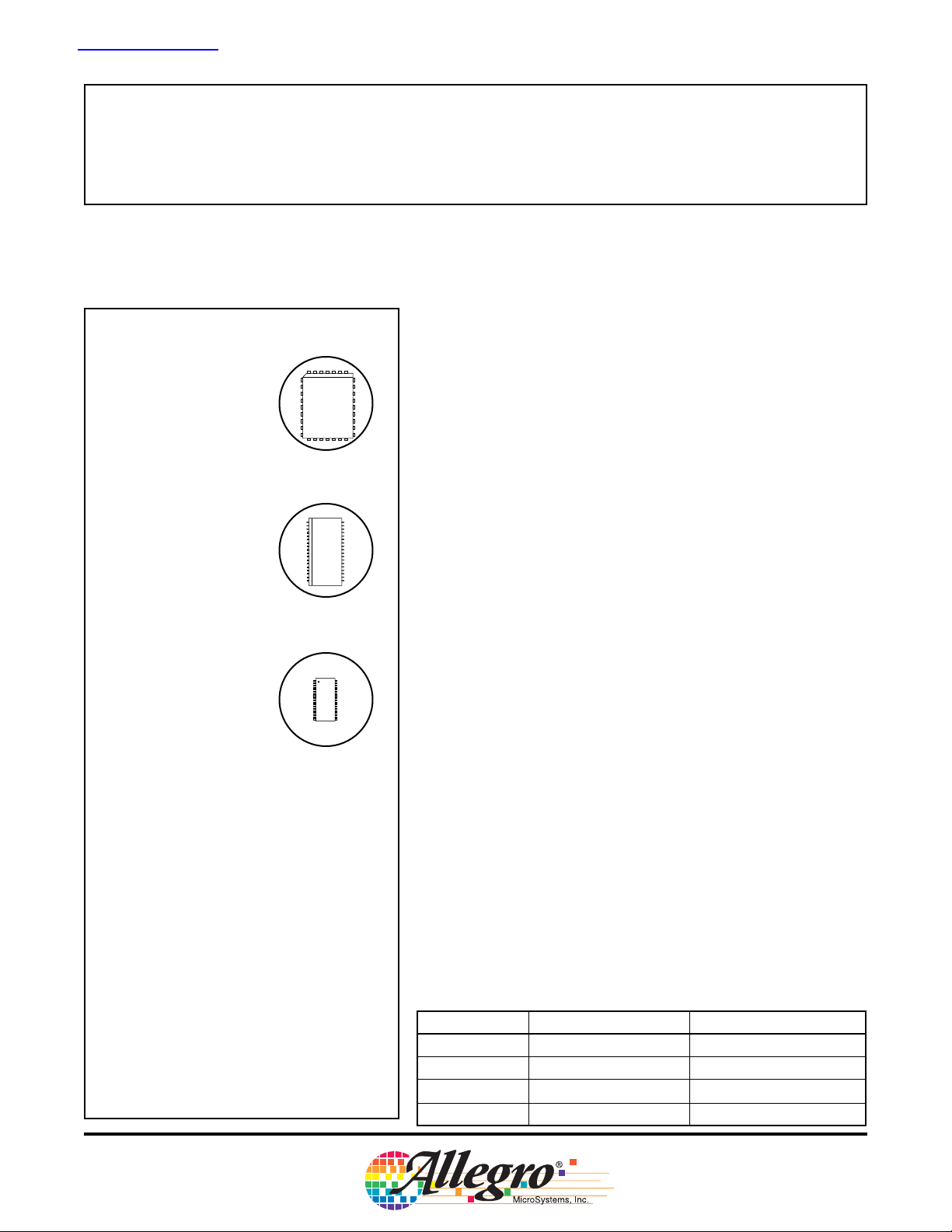
A3938EQ, 32-pin PLCC
A3938LQ, 36-pin QSOP
A3938
Three-Phase Power MOSFET Controller
The A3938 is a three-phase, brushless dc motor controller. The A3938
high-current gate drive capability allows driving of a wide range of
power MOSFETs and can support motor supply voltages to 50 V. The
A3938 integrates a bootstrapped high-side driver to minimize the external component count required to drive N-channel MOSFET drivers.
Internal fi xed off-time, PWM current-control circuitry can be used to
regulate the maximum load current to a desired value. The peak load
current limit is set by the user’s selection of an input reference voltage and external sensing resistor. A user-selected external RC timing
network sets the fi xed off-time pulse duration. For added fl exibility, the
PWM input can provide speed/torque control where the internal current
control circuit sets a limit on the maximum current.
The A3938 includes a synchronous rectifi cation feature. This shorts out
the current path through the power MOSFET reverse body diodes during PWM off-cycle current decay. This can minimize power dissipation
in the MOSFETs, eliminate the need for external power clamp diodes,
and potentially allow a more economical choice for the MOSFET drivers.
26301.104B
Data Sheet
A3938LD, 38-pin TSSOP
AB SO LUTE MAX I MUM RAT INGS
Load Supply Voltage, VBB...................................50 V
VREG (Transient)...............................................15 V
Logic Input Voltage Range, V
Sense Voltage, V
Pins: SA, SB, SC................................... –5 V to 50 V
Pins: GHA, GHB, GHC.................. –5 V to V
Pins: CA, CB, CC ...........................SA/SB/SC + 17 V
Operating Temperature Range
Ambient Temperature, T
Junction Temperature, T
Storage Temperature, TS..........–55°C to +150°C
Thermal Impedance (Typical), at T
measured on a JEDEC-standard "High-K" PCB
A3938EQ, R
A3938LD, R
A3938LQ, R
SENSE
........................................37°C/W
θJA
........................................38°C/W
θJA
........................................44°C/W
θJA
...–0.3 V to V
IN
........................... –5 V to 1.5 V
.............–20°C to +85°C
A
............................+150°C
J
= +25ºC;
A
LCAP
+0.3 V
+ 17 V
BB
The A3938 provides commutation logic for Hall sensors confi gured for
120-degree spacing. The Hall input pins are pulled-up to an internallygenerated 5 V reference. Power MOSFET protection features include:
bootstrap capacitor charging current monitor, regulator undervoltage
monitor, motor lead short-to-ground, and thermal shutdown.
The LD package is available in a lead-free version (100% matte tin
plated leadframe).
FEATURES
Drives wide range of N-channel MOSFETs
Low-side synchronous rectifi cation
Power MOSFET protection
Adjustable dead time for cross-con-
duction protection
Selectable coast or dynamic brake on
power-down or RESET input
Fast/slow current decay modes
Use the following complete part numbers when ordering:
Part Number Pins Package
A3938SEQ 32 PLCC
A3938SLQ 36 QSOP
A3938SLD 38 TSSOP
A3938SLD-T 38 TSSOP, Lead-free
Internal PWM current control
Motor lead short-to-ground
protection
Internal 5 V regulator
Fault diagnostic output
Thermal shutdown
Undervoltage protection
A3938
Three-Phase Power MOSFET Controller
Functional Block Diagram
(This diagram shows only one of the three outputs)
26301.104B
Data Sheet
Short to GND
Logic
TSD
Invalid Hall
VREG Undervoltage
High-Side
Protection
Logic
Low-Side
Protection
Logic
Regulator
Charge Pump
Turn-On
Delay
Turn-On
Delay
VREG
High-Side
Driver
Low-Side
Driver
FAULT
LCAP
+
0.1 uF
H1
H2
H3
PWM
DIR
RESET
BRAKE
MODE
RC
C
T
R
T
O.D.
Control
RC Blanking
Fixed Off-Time
VBB
VREG
CA
GHA
SA
GLA
SENSE
A
C
BOOT
0.1 uF
+
0.1 uF
+
10 uF
To Phase C
To Phase B
REF
DEAD
AGND
VREG
Dead-Time
Adjust
A
For 12 V applications, VBB must be shorted to VREG. For this condition, the absolute
V
REG
RESET
UVLO
Power Loss
Brake
PGND
BRKCAP
BRKSEL
maximum rating of 15 V on VREG must be maintained to prevent damage to the A3938.
www.allegromicro.com
115 Northeast Cutoff, Box 15036
Worcester, Massachusetts 01615-0036 (508) 853-5000
R
S
+
4.7uF
2
A3938
Three-Phase Power MOSFET Controller
26301.104B
Data Sheet
ELECTRICAL CHARACTERISTICS
C
= 10 µF, PWM = 22.5 kHz, square wave, two phases active
VREG
1,2
Unless otherwise noted: T
Characteristics Symbol Test Conditions Min. Typ.
Quiescent Current I
LCAP Regulator V
VREG =VBB Supply Voltage Range V
VBB
LCAP
REG
RESET = 1, Coast mode, stopped – – 8.0 mA
I
lcap
VREG = VBB, observe maximum rating = 15 V 10.8 – 13.2 V
VBB = 13.2 V to 18 V, I
VREG Output Voltage V
VREG Load Regulation V
VREG Line Regulation V
REG
REGLOADIvreg
REGLIN
VBB = 18 V to 50 V, I
I
vreg
Control Logic
Logic Input Voltage
Logic Input Current
V
IN(1)
V
IN(0)
I
IN(1)
I
IN(0)
Minimum high level for logical 1 2.0 – – V
Maximum low level for logical 0 – – 0.8 V
VIN = 2.0 V –30 – –90 µA
VIN = 0.8 V –50 – –130 µA
= 25°C, V
A
= 18 V to 50 V, C
BB
= 0.1 µF, C
LCAP
1
= 0.1 µF,
BOOT
Max. Units
= –3.0 mA 4.75 5 5.25 V
= –10 mA – VBB – 2.5 – V
vreg
= –10 mA 12.4 13 13.6 V
vreg
= –1 mA to –30 mA, Coast mode – 25 – mV
= –10 mA, Coast mode – 40 – mV
Gate Drive
Low-Side Drive, Output High V
High-Side Drive, Output High V
Pull-Up Switch Resistance R
Pull-Down Switch Resistance R
Low-Side Switching, 10/90 Rise Time tr
Low-Side Switching, 10/90 Fall Time tf
High-Side Switching, 10/90 Rise Time tr
High-Side Switching, 10/90 Fall Time tf
Propagation Delay; GHx,GLx Rising T
Propagation Delay; GHx,GLx Falling T
Dead Time, Maximum t
Dead Time, Minimum t
Continued on next page...
HGL
HGH
DS(ON)
DS(ON)
GL
GL
GH
GH
pr
pf
DEAD
DEAD
Igx = 0 V
– 0.8 V
REG
– 0.5 – V
REG
Igx = 0 10.4 11.6 12.8 V
Igx = –50 mA – 14 – Ω
Igx = 50 mA – 4 – Ω
C
= 3300 pF – 120 – ns
load
C
= 3300 pF – 60 – ns
load
C
= 3300 pF – 120 – ns
load
C
= 3300 pF – 60 – ns
load
PWM to gate drive out, C
PWM to gate drive out, C
V
= 0, GHx to GLx, C
dead
I
= 780 µA, GLx to GHx, C
DEAD
= 3300 pF – 220 – ns
load
= 3300 pF – 110 – ns
load
= 0 3.5 5.6 7.6 µs
load
= 0 50 100 150 ns
load
www.allegromicro.com
115 Northeast Cutoff, Box 15036
Worcester, Massachusetts 01615-0036 (508) 853-5000
3
A3938
Three-Phase Power MOSFET Controller
26301.104B
Data Sheet
ELECTRICAL CHARACTERISTICS
C
= 0.1 µF, C
BOOT
Characteristics Symbol Test Conditions Min. Typ.
Bootstrap Capacitor
Bootstrap Capacitor Voltage V
Bootstrap R
OUT
Charge Current (Source) I
Current Limit Circuitry
Input Offset Voltage V
Input Current , Sense pin I
Input Current , Reference pin I
Blank Time t
RC Charge Current I
RC Voltage Threshold
= 10 µF, PWM = 22.5 kHz, square wave, two phases active
VREG
1,2
(continued) Unless otherwise noted: T
R
BLANK
V
V
CX
RC
RCL
RCH
Icx = 0, Vsx = 0, V
CX
Icx = –50 mA – 9 12 Ω
CX
0 V < V
IO
B
B
cmr
0 V < Vcm, V
0 V < Vcm, V
R = 56 kΩ, C = 470 pF – 0.91 – µs
= 13 V 10.4 11.6 12.8 V
reg
< 1.5 V – – ± 5 mV
< 1.5 V – –25 – µA
diff
< 1.5 V – 0 – µA
diff
= 25°C, V
A
= 18 V to 50 V, C
BB
1
= 0.1 µF,
LCAP
Max. Units
100 – – mA
–0.9 –1 –1.1 mA
1.0 1.1 1.2 V
2.7 3.0 3.3 V
Protection Circuitry
Bootstrap Charge Threshold I
Short to Ground, Drain-Source Monitor V
VREG Undervoltage Threshold
Fault Output Voltage
Brake Capacitor Supply Current I
Low Side Gate Voltage V
cx
dsh
UVLO
V
OUT
BRAKE
GLBH
Thermal Shutdown Temperature T
Thermal Shutdown Hysteresis ∆T
1
Typical data are for initial design estimations only, and assume optimum manufacturing and application conditions. Performance may vary for
individual units, within the specifi ed maximum and minimum limits.
2
Negative current is defi ned as conventional current coming out of (sourced from) the specifi ed device terminal.
GHx turns on, and GLx turns off, at I
V
– VSX, high side on 1.3 2.0 2.7 V
BB
V
increasing 9.2 9.7 10.2 V
REG
decreasing 8.6 9.1 9.6 V
V
REG
cx
– –9 – mA
IOL = 1 mA – – 0.5 V
VBB = 8 V, BRKSEL = 1 – 30 – µA
VBB=0, BRKCAP = 8V – 6.6 – V
J
J
– 165 – °C
–10– °C
www.allegromicro.com
115 Northeast Cutoff, Box 15036
Worcester, Massachusetts 01615-0036 (508) 853-5000
4

Three-Phase Power MOSFET Controller
Pin Descriptions
RESET. A logic input that enables the device. Has internal
50 kΩ pull-up to LCAP. Setting RESET to 1 coasts or brakes
the motor, depending on the state of the BRKSEL pin. Setting RESET to 0 enables the gate drive to follow commutation logic. Setting RESET to 1 overrides the BRAKE pin.
GLA/GLB/GLC. Low-side gate drive outputs for external
MOSFET drivers. External series gate resistors can be used
to control slew rate seen at the power driver gate, thereby
controlling the di/dt and dv/dt of Sx outputs.
SA/SB/SC. Directly connected to the motor terminals,
these pins sense the voltages switched across the load. The
pins are also connected to the negative side of the bootstrap
capacitors and the negative supply connections for the fl oat-
ing high-side drivers.
GHA/GHB/GHC. High-side gate drive outputs for
N-channel MOSFET drivers. External series gate resistors
can be used to control slew rate seen at the power driver
gate, thereby controlling the di/dt and dv/dt of Sx outputs.
CA/CB/CC. High-side connections for bootstrap capaci-
tors, providing positive supply for high-side gate drivers. The
bootstrap capacitors are charged to approximately VREG
when the output Sx terminals go low. When the outputs
swing high, the voltages on these pins rise with the outputs to
provide the boosted gate voltages needed for the N-channel
power MOSFETs.
MODE. Logic input to set current-decay mode. In response
to a PWM Off command, Slow Decay mode (MODE = 1)
switches off the high-side FET, and Fast Decay mode
(MODE = 0) switches off the high-side and low-side FETs.
Has an internal 50 kΩ pull-up to LCAP.
H1/H2/H3. Hall sensor inputs with internal, 50 kΩ pull-ups
to LCAP. Confi gured for 120-degree electrical spacing.
DIR. Logic input to reverse rotation (see the table Commu-
tation Truth Table, on the next page). Has internal, 50 kΩ
pull-up to LCAP.
FAULT. Open-drain output to indicate fault condition. Will
be pulled high (usually by 5.1 kΩ external pull-up) for any of
the following fault conditions:
• Invalid Hall sensor input code (coasts the motor).
• Undervoltage condition detected at VREG (coasts or brakes
A3938
the motor depending on stored setting for BRKSEL).
• Thermal shutdown (coasts the motor).
• Motor lead (SA/SB/SC) connected to ground (turns off
only the high-side power MOSFETs).
Only the “short-to-ground” fault is latched, but it is cleared
at each commutation. If the motor has stalled due to a shortto-ground being detected, toggling the RESET pin or repeating a power-up sequence clears the fault.
BRAKE. Logic input for braking function. Setting BRAKE
to 1 turns on low-side MOSFETs, and turns off the high-side
MOSFETs. This effectively shorts the BEMF in the windings
and brakes the motor. Internal 50 kΩ pull-up to LCAP. Setting RESET to 1 overrides this BRAKE pin. See also BRKSEL.
BRKCAP. This pin is for connection of the reservoir
capacitor used to provide the positive power supply for the
sink drive outputs for a power-down condition. This allows
predictable braking, if desired. Using a 4.7 µF capacitor will
provide 6.5 V gate drive for 300 ms. If the power-down braking option is not needed (i.e., BRKSEL = 0), then this pin
should be tied to VREG.
BRKSEL. Logic input to enable/disable braking upon
power-down condition or RESET = 1. Internal 50 kΩ pull-up
to LCAP. Setting BRKSEL to 0 enables Coast mode. Setting
BRKSEL to 1 enables Brake mode.
PWM. Speed control input. Setting PWM to 1 turns on
MOSFETs selected by Hall input logic. Setting PWM to 0
turns off the selected MOSFETs. Keep the PWM input held
high to utilize internal current control circuitry. Internal
50 kΩ pull-up to LCAP.
RC. Analog input. Connection for R
fi xed off-time. CT also sets the BLANK time (see the section
Application Information). It is recommended that the fi xed
off-time should not be less than 10 µs. The resistor should be
in the range between 10 kΩ and 500 kΩ.
VREG. Regulated 13 V supply for the low-side gate drive
and the bootstrap capacitor charge circuit. As a regulator, use
a 10 µF decoupling/storage capacitor (ESR < 1 Ω) from this
pin to AGND, as close to the device pins as possible.
Note: For 12 V applications, the VREG pin should be
shorted to VBB.
and CT to set the
T
26301.104B
Data Sheet
www.allegromicro.com
115 Northeast Cutoff, Box 15036
Worcester, Massachusetts 01615-0036 (508) 853-5000
5

A3938
Three-Phase Power MOSFET Controller
26301.104B
Data Sheet
VBB. Motor power supply connection for the A3938 and
for power MOSFETs. It is good practice to connect a decoupling capacitor from this pin to AGND, as close to the device
pins as possible.
REF. Analog input to current limit comparator. Voltage
applied here sets the peak load current according to the following equation:
I
= V
TRIP
REF
/ R
SENSE
LCAP. 5 V reference to power internal logic and provide
low current for DEAD pin and FAULT pin. Connection for
0.1 µF external capacitor for decoupling.
Commutation Truth Table
H1 H2 H3 DIR GLA GLB GLC GHA GHB GHC SA SB SC
1011001100HI ZLO
1001001010 Z HILO
1101100010LOHIZ
0101100001LOZHI
0111010001 ZLOHI
0011010100HILOZ
1010100001LOZHI
1000010001 ZLOHI
1100010100HILOZ
0100001100HI ZLO
0110001010 Z HILO
0010100010LOHIZ
DEAD. Analog input. A resistor between DEAD and LCAP
is selected to adjust turn-off time to turn-on time. This
delay is needed to prevent cross-conduction in the external
power MOSFETs. See the section Application Information
for details on setting dead time.
SENSE. Analog input to the current limit comparator.
Voltage representing load current appears on this pin. Voltage
transients that are seen at this pin when the drivers turn on
are ignored for period of time, t
BLANK
.
AGND. Analog reference ground.
PGND. Return for low-side gate drivers. This should be
connected to the PCB power ground.
Input Logic
MODE PWM RESET Quadrant Mode of Operation**
0* 0 0 Fast decay
0* 1 0 Fast Decay
1 0 0 Slow decay PWM chop – current decay with both low-side drivers ON.
1 1 0 Slow Decay Selected drivers ON. If current limiting, both low-side drivers ON.
XX 1 X
* Low-side, only, Synchronous Rectifi cation mode.
**See Commutation Truth Table for meaning of “both” and "selected."
PWM chop – current decay with opposite of selected lowside drivers ON.
Selected drivers ON. If current limiting, opposite of selected
low-side drivers ON.
All high-side drivers OFF, low-sides see BRKSEL stored.
Clears storable faults.
www.allegromicro.com
115 Northeast Cutoff, Box 15036
Worcester, Massachusetts 01615-0036 (508) 853-5000
6

A3938
Three-Phase Power MOSFET Controller
Application Information
26301.104B
Data Sheet
Synchronous Rectifi cation. To reduce power con-
sumption in the external MOSFETs, during the load current
recirculation PWM-off cycle, the A3938 control logic turns
on the appropriate low-side driver only. The reverse body
diode of the power MOSFET conducts only during the dead
time required at each PWM transition, as usual. However,
unlike full synchronous rectifi cation, the opposite high-side
FET’s body diode (not the RdsON) will carry the re-circulating current, be self-extinguishing, and not force the motor to
reverse direction.
Dead Time. To prevent cross-conduction, it is required to
have a delay between a high-side or low-side turn-off, and
the next turn-on event. The potential for cross-conduction
occurs with synchronous rectifi cation, direction changes,
PWM, or after a bootstrap capacitor charging cycle. This
dead-time is set via a resistor from the DEAD pin to LCAP
and can be varied from 100 ns to 5.5 µs.
For a nominal case, given:
• 25°C ambient temperature, and
• 5.6 kΩ < R
For predicting worst-case overvoltage and temperature
extremes, use the following equations:
t
t
For nominal comparison with I
ambient temperature:
where V
Rather than use R
which activates an internal (I
The choice of power MOSFET and external gate resistance
determines the selection of the dead-time resistor. The dead
time should be made long enough to cover the variation of
the MOSFET capacitance and gate resistor tolerances (both
external and internal to the A3938).
< 470 kΩ,
dead
t
dead (nom,ns)
dead (min,ns)
lcap
= 37 + [(11.9 ×10⁻³) × (R
= 10 + [(6.55 ×10⁻³) × (R
dead (max,ns)
= 63 + [(17.2 ×10⁻³) ×(R
I
dead
= (V
– Vbe) / (R
lcap
= 5 V, Vbe = 0.7 V, and R
values near 470 kΩ, set V
dead
+ 500)]
dead
+ 350)]
dead
+ 650)]
dead
currents, also at 25°C
dead
+ R
dead
= 500 Ω.
int
= 10 µA) current source.
dead
)
int
dead
= 0 V,
Decoupling. The internal reference VREG supplies
current for the gate drive circuit. As the gates are driven
high, they will require current from an external decoupling
capacitor to support the transients. This capacitor should be
placed as close as possible to the VREG pin. The value of the
capacitor should be at least 20 times larger than the bootstrap
capacitor. Additionally, a 1 nF (or larger) ceramic monolithic
capacitor should be connected between LCAP and AGND, as
close to the device pins as possible.
Protection Circuitry. The A3938 has several protection
features:
• Bootstrap Monitor. The bootstrap capacitor is charged
whenever a sink-side MOSFET is on, an Sx output goes low,
or load current recirculates. This happens constantly during
normal operation.
Note: The high side will not be allowed to turn on before the
charging has decayed to less than approximately 9 mA.
• Undervoltage. VREG supplies the low-side gate driver
and the bootstrap charge current. It is critical to ensure that
the voltages are at a proper level before enabling any of the
outputs. The undervoltage circuit is active during power-up
and signals a fault, and also coasts or brakes (depending
on the stored BRKSEL setting) the motor during that time
period, until VREG is greater than approximately 10 V. On
powering down, a fault is signaled and the motor is coasted
or braked, depending on the stored setting for BRKSEL.
• Hall Invalid. Illegal codes for the Hall sensor inputs (0,0,0
or 1,1,1) force a fault and coast the motor. Noisy Hall lines
may cause Hall code errors, and therefore faults. Additional
external pull-up loading and fi ltering may be required in
some systems.
Hint: Use dividers to the VREG terminal, than to the LCAP
terminal, because the VREG terminal has more current
capability.
• Thermal Shutdown. Junction temperatures greater than
165°C cause the A3938 to signal a fault and coast the motor.
• Motor Lead. The A3938 signals a fault if the motor lead
is shorted to ground. A short-to-ground is assumed after a
high- side is turned on and greater than 2 V is measured
between the drain (VBB) and source (Sx) of the high-side
power MOSFET. This fault is cleared at the beginning of
www.allegromicro.com
115 Northeast Cutoff, Box 15036
Worcester, Massachusetts 01615-0036 (508) 853-5000
7

A3938
Three-Phase Power MOSFET Controller
26301.104B
Data Sheet
each commutation. If a stalled motor results from a fault, the
fault can only be cleared by toggling the RESET pin or by a
power-up sequence.
Current Regulation. Load current can be regulated by
an internal fi xed off-time, PWM-control circuit. When the
outputs of the MOSFETs are turned on, current increases in
the motor winding until it reaches a value given by:
I
= V
TRIP
At the trip point, the sense comparator resets the source
enable latch, turning off the source driver. At this point, load
inductance causes the current to recirculate for the fi xed off-
time period. The current path during recirculation is determined by the confi guration of the MODE and SR input pins.
The fi xed off-time is determined by an external resistor, R
and capacitor, CT, connected in parallel from the RC terminal
to AGND. The fi xed off-time is approximated by:
t
OFF
t
should be in the range between 10 µs and 50 µs. Larger
OFF
values for t
could result in audible noise problems. For
OFF
proper circuit operation, 10 kΩ < R
Torque control can be implemented by varying the REF input
voltage as long as the PWM input stays high. If direct control
of the torque/current is desired by PWM input, a voltage can
be applied to the REF pin to set an absolute maximum current limit.
PWM Blank. The capacitor C
to set the BLANK time duration. At the end of a PWM
off-cycle, a high-side gate selected by the commutation logic
turns on. At this time, large current transients can occur during the reverse recovery time, trr, of the intrinsic body diodes
/ R
REF
SENSE
= RT × C
T
< 500 kΩ.
T
also serves as the means
T
,
T
of the power MOSFETs. To prevent false tripping of the
sense comparator, the BLANK function disables the comparator for a time period defi ned by:
t
BLANK
= 1.9 × C
/ (1 × 10⁻³ – [2 / RT])
T
The user must ensure that CT is large enough to cover the
current spike duration.
Braking. The A3938 dynamically brakes the motor by
forcing all low-side power MOSFETs on, and all high-side
power MOSFETs off. This effectively short-circuits the
BEMF and brakes the motor. During braking, the load current can be approximated by:
I
BRAKEPEAK
= V
BEMF
/ R
LOAD
As the current does not fl ow through the sense resistor dur-
ing a dynamic brake, care should be taken to ensure that the
maximum ratings of the power MOSFETs are not exceeded.
Note: On its rising edge, a RESET setting of 1 overrides the
BRAKE input pin and latches the condition selected by the
BRKSEL pin.
Power Loss Brake. The BRKCAP and BRKSEL pins
provide a power-down braking option. A Power-Loss Brake
Trigger Event, which is either an undervoltage on VREG
or a RESET = 1 rising edge, is sensed by the A3938, which
then dynamically brakes or coasts (depending on the stored
BRKSEL setting) the motor. The reservoir capacitor on the
BRKCAP pin provides the positive voltage that forces the
low-side gates of the power MOSFETs high, keeping them
on, even after supply voltage is lost. A stored setting of BRKSEL = 1 brakes the motor, but a stored setting of BRKSEL = 0
coasts it. The combined effect of these settings is shown in the
table Brake Control.
Brake Control
BRAKE BRKSEL Before Power Loss Brake Trigger Event After Power Loss Brake Trigger Event
0 0 Normal run mode Coast mode – All gate drive outputs OFF
0 1 Normal run mode Brake mode – All low-side gate drivers ON
1 0 Brake mode – All low-side gate drivers ON Coast mode – All gate drive outputs OFF
1 1 Brake mode – All low-side gate drivers ON Brake mode – All low-side gate drivers ON
www.allegromicro.com
115 Northeast Cutoff, Box 15036
Worcester, Massachusetts 01615-0036 (508) 853-5000
8

Three-Phase Power MOSFET Controller
Terminal List
32-Lead
Name Description
PGND Low-Side Gate Drive Return 1 36 36
RESET Control Input 2 1 1
GLC Low-Side Gate Drive Output, Phase C 3 2 2
SC Motor Connection, Phase C 4 3 3
GHC High-Side Gate Drive Output, Phase C 5 6 6
CC Bootstrap Capacitor, Phase C 6 7 7
GLB Low-Side Gate Drive Output, Phase B 7 8 8
SB Motor Connection, Phase B 8 9 9
GHB High-Side Gate Drive Output, Phase B 9 10 10
CB Bootstrap Capacitor, Phase B 10 11 11
GLA Low-Side Gate Drive Output, Phase A 11 12 12
SA Motor Connection, Phase A 12 13 13
GHA High-Side Gate Drive Output, Phase A 13 14 14
CA Bootstrap Capacitor, Phase A 14 15 15
VREG Gate Drive Supply 15 16 16
LCAP 5 V Output 16 17 17
FAULT Diagnostic Output 17 19 19
MODE Control Input 18 20 20
VBB Load Supply 19 21 21
H1 Hall Control Input 20 22 22
H3 Hall Control Input 21 24 24
H2 Hall Control Input 22 25 25
DIR Control Input 23 26 26
BRAKE Control Input 24 27 27
BRKCAP Power Loss Brake Reservoir Capacitor 25 28 28
BRKSEL Control Input 26 29 29
PWM Control Input 27 30 30
RC Connection for Fixed Off-Time R and C 28 31 31
SENSE Sense Resistor 29 32 32
REF Current Limit Adjust 30 33 33
DEAD Dead Time Adjust 31 34 34
AGND Ground 32 35 35
N/C Not Connected 4,5,18,23
A3938EQ
PLCC
36-Lead
A3938LQ
QSOP
A3938
38-Lead
A3938LD
TSSOP
4, 5, 18,
23, 37, 38
26301.104B
Data Sheet
www.allegromicro.com
115 Northeast Cutoff, Box 15036
Worcester, Massachusetts 01615-0036 (508) 853-5000
9

SC
4
GLC
3
RESET
PGND
2
1
AGND
DEAD
323130
A3938
Three-Phase Power MOSFET Controller
A3938EQ, 32-pin PLCC
.495
12.57
.485
12.32
.453
11.51
.447
REF
11.35
132
.013
.008
0.32
0.19
26301.104B
Data Sheet
GHC
CC
GLB
SB
GHB
CB
GLA
SA
GHA
RESET
GLC
N/C
N/C
GHC
CC
GLB
GHB
GLA
GHA
VREG
LCAP
N/C
SC
SB
CB
SA
CA
5
6
7
8
9
10
11
12
13
14
CA
Control
Fault
1617181920
15
LCAP
VREG
FAULT
Logic
MODE
VBB
29
SENSE
28
RC
27
PWM
26
BRKSEL
25
BRKCAP
24
BRAKE
23
DIR
22
H2
21
H3
H1
.595
.585
15.11
14.86
.553
14.05
.547
13.89
.021
0.53
.013
0.33
.050
1.27
BSC
Dimensions in inches
Metric dimensions (mm) in brackets, for reference only
If unit is intended to be socketed, it is advisable to review lead profile with socket supplier
.095
.060
.140
.125
2.41
1.52
3.56
3.18
.015
0.38
MIN
Seating Plane
Base Plane
A3938LQ, 36-pin QSOP
.606
15.40
.598
0.80
REF
15.20
.031
0.30
0.10
1
2
3
4
5
6
7
8
9
10
11
12
13
14
15
16
17
18
Control
Fault
Logic
36
35
34
33
32
31
30
29
28
27
26
25
24
23
22
21
20
19
PGND
AGND
DEAD
REF
SENSE
RC
PWM
BRKSEL
BRKCAP
BRAKE
DIR
H2
H3
N/C
H1
VBB
MODE
FAULT
10.51
10.11
0.85
BSC
0.51
0.28
.414
.398
36
.299
7.60
.291
7.40
21
.020
.011
.033
Dimensions in millimeters
U.S. Customary dimensions (in.) in brackets, for reference only
2.64
2.44
.012
.004
8º
0º
0.32
0.23
1.27
0.40
.355
BSC
Seating Plane
Gauge Plane
.104
.096
0.014
.013
.009
.050
.016
www.allegromicro.com
115 Northeast Cutoff, Box 15036
Worcester, Massachusetts 01615-0036 (508) 853-5000
10

RESET
GLC
SC
N/C
N/C
GHC
CC
GLB
SB
GHB
CB
GLA
SA
GHA
CA
VREG
LCAP
N/C
FAULT
26301.104B
Data Sheet
A3938
Three-Phase Power MOSFET Controller
A3938LD, 38-pin TSSOP
9.8
0.386
9.6
.50
BSC
.020
0.378
0.75
0.45
0.030
0.018
0.15
0.05
1.10
MAX
0.006
0.002
0.043
1
2
3
4
5
6
7
8
9
10
11
12
13
14
15
16
17
18
19
Control
Fault
Logic
38
37
36
35
34
33
32
31
30
29
28
27
26
25
24
23
22
21
20
N/C
N/C
PGND
AGND
DEAD
REF
SENSE
RC
PWM
BRKSEL
BRKCAP
BRAKE
DIR
H2
H3
N/C
H1
VBB
MODE
6.4
BSC
0.252
0.27
0.17
38
4.5
0.177
4.3
0.169
21
0.011
0.007
Dimensions in millimeters
U.S. Customary dimensions (in.) in brackets, for reference only
8º
0º
0.20
0.09
1
0.039
REF
.25
0.010
BSC
Seating Plane
Gauge Plane
0.008
0.004
The products described here are manufactured under one or
more U.S. patents or U.S. patents pending.
Allegro MicroSystems, Inc. reserves the right to make, from time
to time, such de par tures from the detail spec i fi ca tions as may be
required to permit improvements in the per for mance, reliability,
or manufacturability of its products. Before placing an order, the
user is cautioned to verify that the information being relied upon is
current.
Allegro products are not authorized for use as critical components in life-support devices or sys tems without express written
approval.
The in for ma tion in clud ed herein is believed to be ac cu rate and
reliable. How ev er, Allegro MicroSystems, Inc. assumes no re spon si bil i ty for its use; nor for any in fringe ment of patents or other
rights of third parties which may result from its use.
Copyright©2003 AllegroMicrosystems, Inc.
www.allegromicro.com
115 Northeast Cutoff, Box 15036
Worcester, Massachusetts 01615-0036 (508) 853-5000
11
 Loading...