

Allegro A3933SEQ Datasheet
GHC
GLB
GHB
GLA
GHA
26301.100†
Data Sheet
3933
THREE-PHASE POWER
MOSFET CONTROLLER
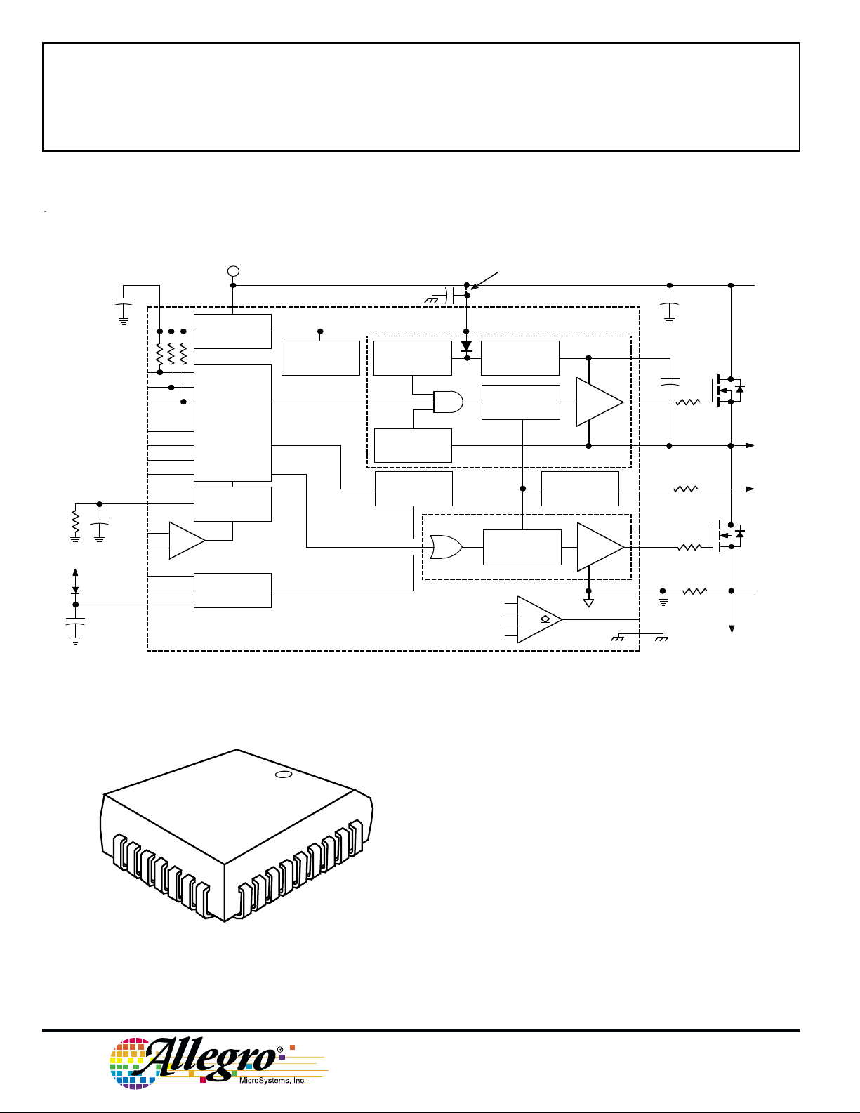
The A3933SEQ is a three-phase MOSFET controller for use with
SC
GLC
3
4
5
6
CC
7
8
SB
9
10
CB
11
12
SA
13
14
15
CA
VCCOUT
RESET
2
16
LCAP
PGND
1
FAULT
17
FAULT
DEAD
AGND
31
32
CONTROL LOGIC
18
19
VBB
MODE
REF
30
BRAKE
20
H1
29
28
27
26
25
24
23
19
22
21
Dwg. PP-068
SENSE
RC
PWM
BRKSEL
BRKCAP
BRAKE
DIR
H2
H3
bipolar brushless dc motors. It drives all n-channel external power
r
FETs, allowing system cost savings and minimizing
(DS)on
power loss.
The high-side drive block is implemented with bootstrap capacitors at
each output to provide the floating positive supply for the gate drive.
The high-side circuitry also employs a unique “intelligent” FET
monitoring circuit that ensures the gate voltages are at the proper levels
before turn-on and during the ON cycle. This device is targeted for
applications with motor supplies from 12 V to 28 V.
Internal fixed off-time PWM current-control circuitry can be used to
regulate the maximum load current to a desired value. The peak loadcurrent limit is set by the user’s selection of an input reference voltage
and external sensing resistor. The fixed off-time pulse duration is set
by a user-selected external RC timing network.
A power-loss braking circuit brakes the motor on an under-voltage
condition. The device is configured to either coast or dynamically
brake the motor when this occurs.
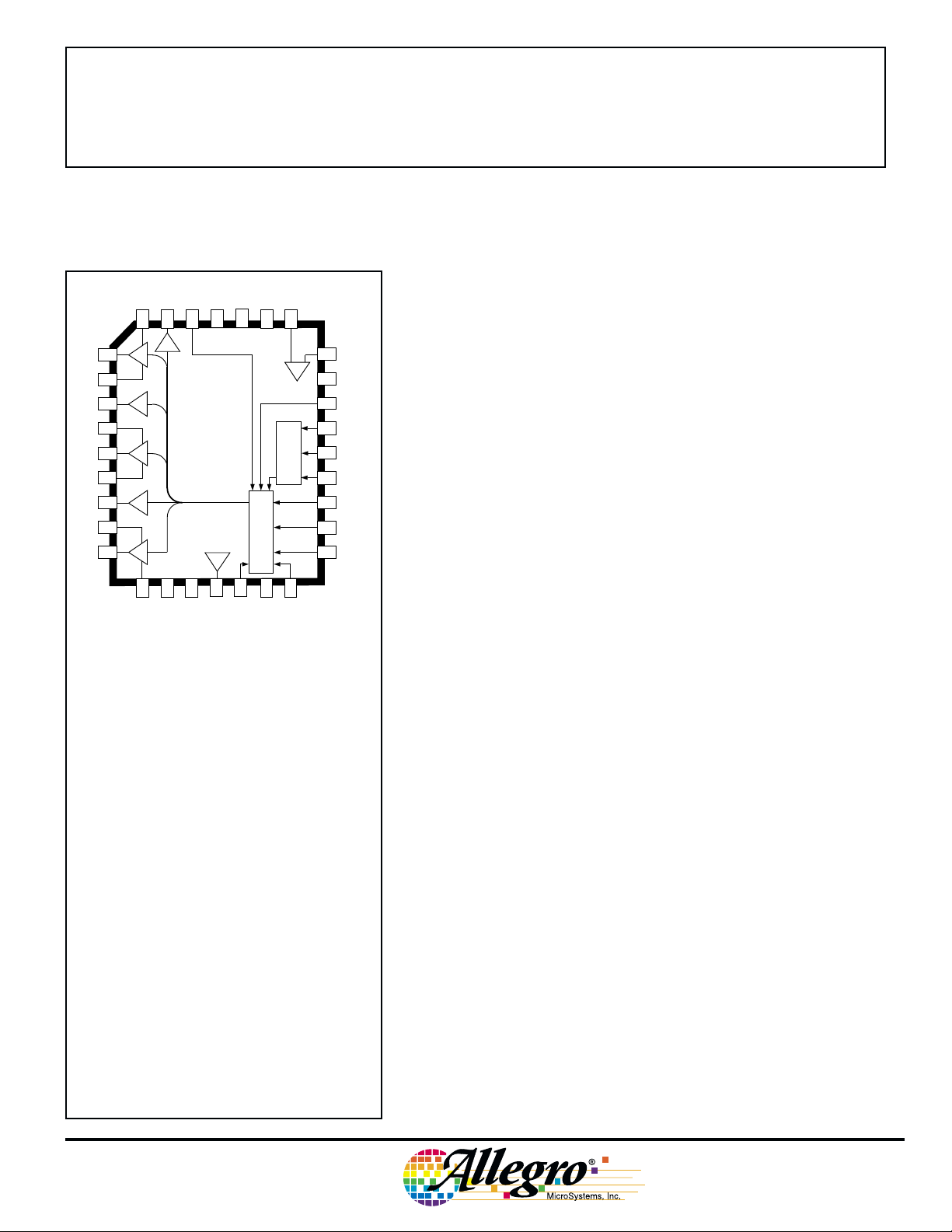
The A3933SEQ is supplied in a 32-lead rectangular (9 x 7) plastic
chip carrier (quad pack) for minimum-area, surface-mount applications.
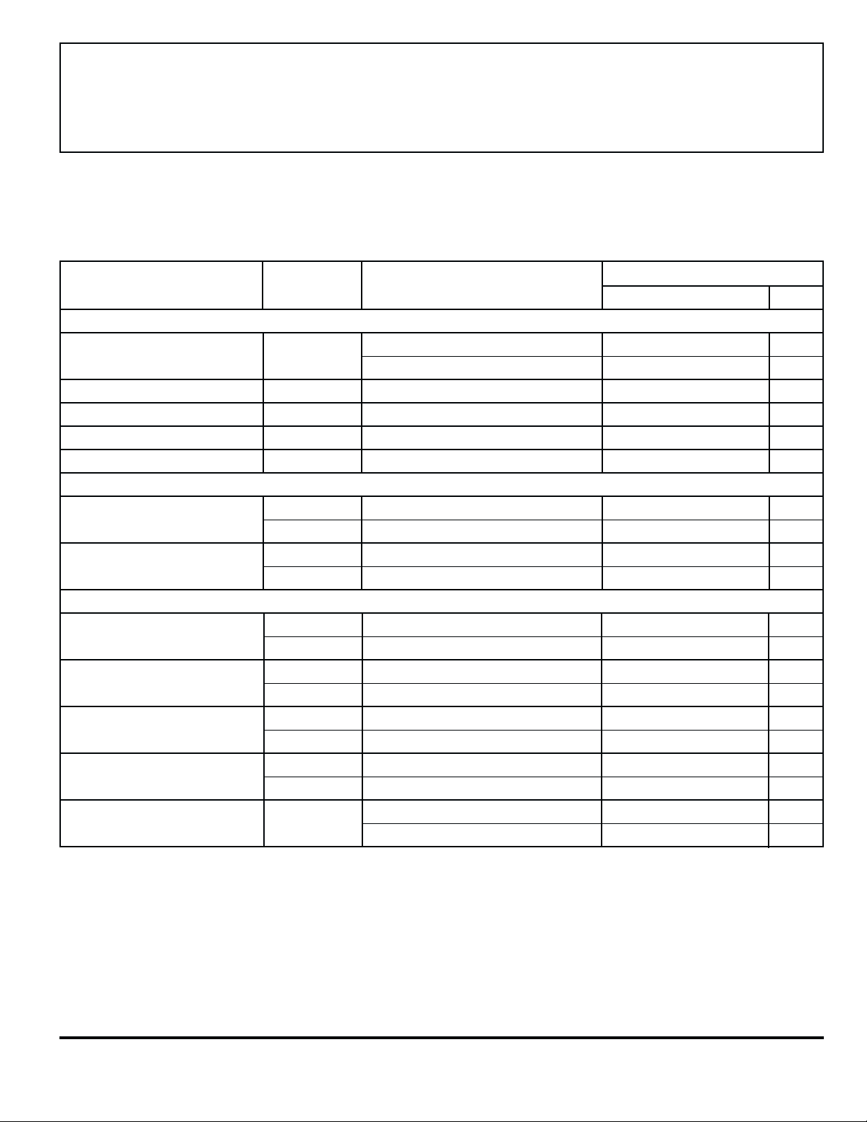
ABSOLUTE MAXIMUM RATINGS
at TA = 25°C
Supply Voltage, VBB............................. 28 V
(peak) .............................................. 30 V
Terminal Voltage, V
(peak) .............................................. 15 V
Logic Input Voltage Range,
VIN.................. -0.3 V to V
Sense Voltage Range,
V
............................. -5 V to V
SENSE
Output Voltage Range,
VSA, VSB, VSC.................. -5 V to +30 V
V
, V
GHB
, V
GHC
GHA
VCA, VCB, VCC..................... VSX + 14 V
Operating Temperature Range,
TA................................. -20°C to +85°C
Junction Temperature, TJ................. +150°C
Storage Temperature Range,
TS............................... -55°C to +150°C
................. 13.2 V
CCOUT
LCAP
. -5 V to VBB + 14 V
+ 0.3 V
LCAP
FEATURES AND BENEFITS
■ Drives External N-Channel FETs
■ Intelligent High-Side Gate Drive
■ Selectable Coast or Dynamic Brake on Power Down
■ Adjustable Dead Time for Cross-Conduction Protection
■ Selectable Fast or Slow Current-Decay Modes
■ Internal PWM Peak Current Control
■ Reset/Coast Input
■ 120° Hall Commutation with Internal Pullup
■ Internal 5-V Regulator
■ Low-Side Synchronous Rectification
■ Direction Control
■ PWM Speed-Control Input
■ Fault-Diagnostic Output
■ Under-Voltage Protection
3933
THREE-PHASE POWER
MOSFET CONTROLLER
Functional Block Diagram
V
TO
CCOUT
RTC
DIR
RESET
MODE
PWM
T
REF
SENSE
BRAKE
BRKSEL
BRKCAP
H1
H2
H3
RC
LCAP
+
–
+V
V
BB
REGULATOR
CONTROL
LOGIC
RC BLANKING
(FIXED OFF TIME)
BRAKE
UNDER-
VOLTAGE
DETECT
BOOTSTRAP
MONITOR
GATE-SOURCE
MONITOR
LOW-SIDE
SYNCHRONOUS
RECTIFICATION
1 OF 3 LOW-SIDE DRIVERS
BOOTSTRAP LOW
UNDERVOLTAGE
V
CCOUT
V
GS
LOW
INVALID HALL
CONNECT FOR
12-V OPERATION
BOOTSTRAP
CHARGE
TURN-ON
DELAY
1 OF 3 HIGH-SIDE DRIVERS
TURN-ON
DELAY
HIGH-SIDE
DRIVER
DEAD-TIME
ADJUST
LOW-SIDE
DRIVER
C
X
GH
X
S
X
DEAD
GL
X
PGND
FAULT
AGND
C
boot
TO
1 OF 3
MOTOR
PHASES
TO
LCAP
R
S
TO
SENSE
Dwg. FP-045
Dwg. OA-007-32
115 Northeast Cutoff, Box 15036
Worcester, Massachusetts 01615-0036 (508) 853-5000
Copyright © 1999, Allegro MicroSystems, Inc.
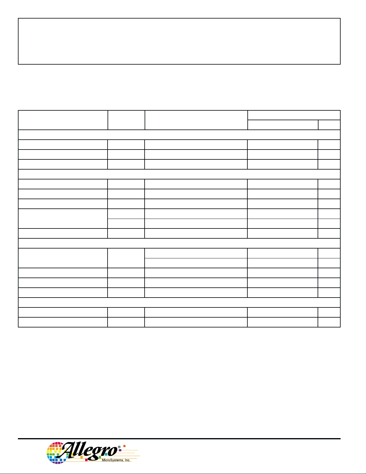
RECOMMENDED OPERATING CONDITIONS
Supply Voltage, VBB...................................... 15 V to 28 V
or, if VBB = V
Logic Input Voltage Range, VIN.............. -0.3 V to +4.8 V
Sense Voltage Range, V
RC Resistance .......................................... 10 kΩ to 100 kΩ
PWM Frequency, f
................................... 12 V ±10%
CCOUT
........................ -1 V to +1 V
SENSE
....................... 20 kHz to 100 kHz
PWM
3933
THREE-PHASE POWER
MOSFET CONTROLLER
ELECTRICAL SPECIFICATIONS at TA = 25°C, VBB = V
CCOUT
= 12 V, C
= 1000 pF, C
load
= 0.047 µF
boot
(unless noted otherwise).
Limits
Parameter Symbol Conditions Min Typ Max Units
Supply Current
Quiescent Current I
Reference Voltage V
Ref. Volt. Load Regulation ∆V
LCAP(∆ILCAP)ILCAP
Output Voltage V
Output Voltage Regulation
∆V
CCOUT(∆ICCOUT)VBB
BB
LCAP
CCOUT
RESET low, f
= 40 kHz – 16 19 mA
PWM
RESET high – 15 17 mA
4.75 5.0 5.25 V
= 0 to -2 mA – 10 25 mV
VBB = 28 V 10.8 12 13.2 V
= 28 V, I
= 0 to -10 mA – – 25 mV
CCOUT
Digital Logic Levels
Logic Input Voltage V
Logic Input Current I
IH
V
IL
IH
I
IL
VIH = 2 V – <1.0 10 µA
VIL = 0.8 V -70 – -130 µ A
2.0 – – V
––0.8V
Gate Drive
Low-Side Output Voltage V
High-Side Output Voltage V
Low-Side Output t
Switching Time
High-Side Output t
Switching Time
DEAD Time t
(Source OFF to Sink ON)
GLxH
V
GLxL
GHxH
V
GHxL
rGLx
t
fGLx
rGHx
t
fGHx
DEAD
I
= 1 mA – – 0.30 V
GLx
I
= 1 mA – – 0.25 V
GHx
1 V to 8 V – 50 – ns
8 V to 1 V – 40 – ns
1 V to 8 V – 100 – ns
8 V to 1 V – 100 – ns
I
= 10 µA – 3000 – ns
DEAD
I
= 215 µA – 180 – ns
DEAD
9.5 10.5 11.5 V
9.0 10.5 11.5 V
NOTES: 1. Typical Data is for design information only.
2. Negative current is defined as coming out of (sourcing) the specified device terminal.
www.allegromicro.com
Continued —
3933
THREE-PHASE POWER
MOSFET CONTROLLER
ELECTRICAL SPECIFICATIONS at TA = 25°C, VBB = V
CCOUT
= 12 V, C
= 0.001 µF, C
load
= 0.047 µF
boot
(unless noted otherwise), continued.
Limits
Parameter Symbol Conditions Min Typ Max Units
Bootstrap Capacitor
Bootstrap Charge Current I
Bootstrap Output Voltage V
Leakage Current I
Cx
Cx
Cx
Reference Sx 9.5 10.5 11.5 V
High side switched high, Sx = V
BB
50 100 150 mA
–1520 µA
Current Limit
Offset Voltage V
Input bias current I
SENSE
RC Charge Current I
RC Voltage Threshold V
V
PWM frequency Range f
io
RC
RCL
RCH
PWM
Operating 20 – 100 kHz
–0±5.0 mV
– – -1.0 µA
850 945 1040 µA
1.0 1.1 1.2 V
2.7 3.0 3.2 V
Protection Circuitry
Undervoltage Threshold UVLO Increasing V
Decreasing V
Boot-Strap Capacitor Volt. V
High-Side Gate-Source Volt. V
Fault Output Voltage V
CxSx
GHxSx
FAULT
VBB = 12 V 9.5 – – V
IO = 1 mA – – 0.8 V
BB
BB
9.7 10.2 10.7 V
9.35 – 10.35 V
–6.3– V
Brake Function
Brake Cap. Supply Current I
Low-Side Gate Voltage V
BRKCAP
GLxH
VBB = 8 V, BRKSEL ≥ 2 V – 30 – µA
V
= 0, BRKCAP = 8 V – 6.6 – V
BB
NOTES: 1. Typical Data is for design information only.
2. Negative current is defined as coming out of (sourcing) the specified device terminal.
115 Northeast Cutoff, Box 15036
Worcester, Massachusetts 01615-0036 (508) 853-5000
 Loading...