

Allegro A3932SEQ Datasheet
ADVANCED DATASHEET - 03/02/99
(Subject to change without notice)
SC
GLC2RESET1PGND32AGND31DEAD30REF
4
3
29
GHC
CC
GLB
GHB
CB
GLA
GHA
5
6
7
8
SB
A3932SEQ
9
10
11
12
SA
13
14 CA
15 VREG
16 LCAP
17 FAULT
18 MODE
19 VBB20 H1
SENSE
28
RC
27
PWM
26
TACH
25
SR
24
BRAKE
23
DIR
22
H2
21
H3
Page 1 of 8
3932
THREE PHASE POWER
MOSFET CONTROLLER
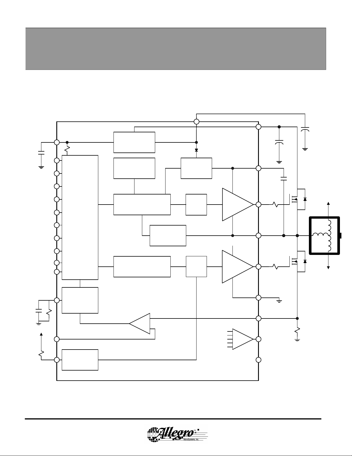
The A3932SEQ is a three-phase brushless DC motor controller. The
A3932’s high current gate drive capability allows driving of a wide range of
power MOSFETs and can support motor supply voltages from 12 to 50V.
The A3932 integrates a bootstrapped high side driver to minimize the
external component count required to drive N-channel MOSFET drivers.
Internal fixed off time PWM current control circuitry can be used to
regulate the maximum load current to a desired value. The peak load current
limit is set by the user’s selection of an input reference voltage and external
sensing resistor. The fixed off time pulse duration is set by a user-selected
external RC timing network. For added flexibility, the PWM input can be
used to provide speed/torque control, allowing the internal current control
circuit to set a maximum current limit.
ABSOLUTE MAXIMUM RATINGS
at TA = +25°C
Load Supply Voltage, VBB............................50 V
VREG (Transient) ......................................... 15 V
Logic Input Voltage Range,
VIN...................-0.3 V to V
Sense Voltage, V
........................ -5 to 1.5 V
SENSE
Pins SA/SB/SC, ................................... -5 to 50 V
Pins GHA/GHB/GHC................-5 to VBB + 17 V
Pins CA/CB/CC.........................SA/SB/SC+17 V
Package Power Dissipation (TA = +25°C)
R
..................................... 52.4 °°C/W
ØJA
R
..................................... 22.7 °°C/W
ØJC
PD................................................2.4 W
Operating Temperature Range,
TA................................-20°°C to +85°°C
Junction Temperature, TJ.........................+150°°C
Storage Temperature Range,
TS...............................-55°°C to +150°°C
LCAP
+ 0.3 V
The A3932 includes optional synchronous rectification. This feature
will short out the current path through the power MOSFETs intrinsic body
diodes during PWM off cycle current decay. This can minimize power
dissipation in the MOSFETs, eliminate the need for external power clamp
diodes, and potentially allow a more economical choice for the MOSFET
drivers.
The A3932 provides commutation logic for Hall sensors configured
for 120-degree spacing. The Hall input pins are pulled up to an internally
generated 5V reference. Power MOSFET protection features includes gatesource voltage monitor, bootstrap capacitor charging current monitor,
undervoltage monitor, motor lead short to supply or ground, and thermal
shutdown.
FEATURES
n Drives Wide Range of N-channel
MOSFETs
n Sources 1.25A for Gate Turn-On
n Sinks 2.5A for Gate Turn-Off
n Synchronous Rectification
n Power MOSFET Protection
n Adjustable Dead Time for Cross
Conduction Protection
n Fast/Slow Current Decay Modes
n Internal PWM current Control
n PWM Torque Control Input
n Motor Lead Short to Supply
and Ground Protection
n Internal 5V Regulator
n Direction Control
n Brake Input
n Fault Diagnostic Output
n Tachometer Output
n Thermal Shutdown
n Undervoltage Protection
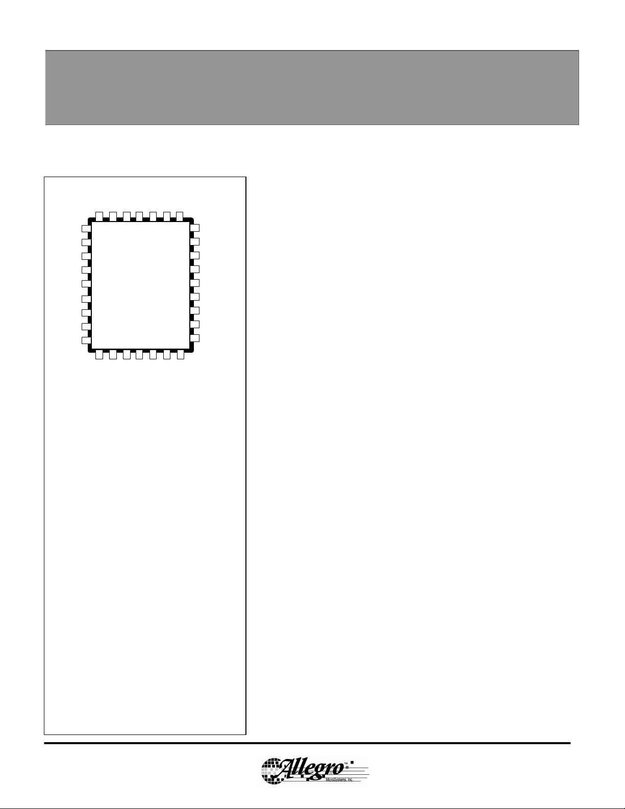
n 32L PLCC Package
Always order by complete part number: A3932SEQ
3932
THREE-PHASE POWER MOSFET CONTROLLER
Functional Block Diagram (1 of 3 outputs shown)
Page 2
LCAP
H1
H2
H3
PWM
DIR
RESET
SR
BRAKE
MODE
TACH
Control
Logic
Regulator
Undervoltage
Detect
High Side Protection
Logic
Gate-Source
Monitor
Low Side Protection
Logic
VREG
Bootcap
Monitor
Turn-on
Delay
Turn-on
Delay
High
Side
Driver
VREG
Low
Side
Driver
VBB
CA
GHA
SA
GLA
C
BOOT
To Phase C
To Phase B
C
T
to LCAP
DEAD
RC
REF
R
T
RC Blanking
Fixed - Off
Time
Dead-Time
Adjust
PGND
+
Bootstrap low
Vgs Low
Motor Lead Short
Invalid Hall
Undervoltage
SENSE
FAULT
AGND
R
S
3932
THREE-PHASE POWER MOSFET CONTROLLER
Page 3
ELECTRICAL CHARACTERISTICS at TA = +25°C, VBB = 50 V, C
BOOT
= .1µf, C
=1000pf (unless noted otherwise)
LOAD
Characteristics Symbol Test Conditions Min. Typ. Max. Units
I
Quiescent current
LCAP Regulator V
VBB
I
VBB
LCAP
Motor Supply Voltage Range 18 – 50 V
VREG Output Voltage V
VREG Line Regulation V
REG
REGLIN
RESET Low 6.5 8.5 mA
RESET High 6.5 mA
4.75 5 5.250 V
VREG shorted to V
BB
10.8 – 13.2 V
12.4 13 13.6 V
VBB 18 to 50V – 40 – mV
Control Logic
Logic Input Voltage V
Logic Input Current I
V
I
IN(1)
IN(0)
IN(1)
IN(0)
VIN = 2.0 V – <1.0 10 µA
VIN = 0.8 V -70 – -130 µA
2.0 – – V
– – .8 V
Gate Drive
Low side drive, output high V
High side drive, output high V
Pull Up Switch Resistance R
Pull Down Switch Resistance R
Low side switching, rise time tr
Low side switching, fall time tf
High side switching, rise time tr
High side switching, fall time tf
Dead time maximum t
Dead time minimum t
HGL
HGH
DS(ON)
DS(ON)
GL
GL
GH
GH
DEAD
DEAD
-1A transient 6 9 12 Ω
2.5A transient 2 3 4 Ω
10% to 90% – 25 – ns
I
= 9µA – 5500 – ns
DEAD
I
= 780µA – 100 – ns
DEAD
NOTES:
1. Typical Data is for design information only.
2. Negative current is defined as coming out of (sourcing) the specified device pin.
12.3 13 13.7 V
10.5 11.6 12.8 V
– 10 – ns
– 40 – ns
– 10 – ns
 Loading...