

A3930 and A3931
Automotive 3-Phase BLDC Controller and MOSFET Driver
Features and Benefits
High current 3-phase gate drive for N-channel MOSFETs
Synchronous rectification
Cross-conduction protection
Charge pump and top-off charge pump for 100% PWM
Integrated commutation decoder logic
Operation over 5.5 to 50 V supply voltage range
Extensive diagnostics output
Provides +5 V Hall sensor power
Low-current sleep mode
Package: 48 Lead LQFP with exposed
thermal pad (suffix JP)
Description
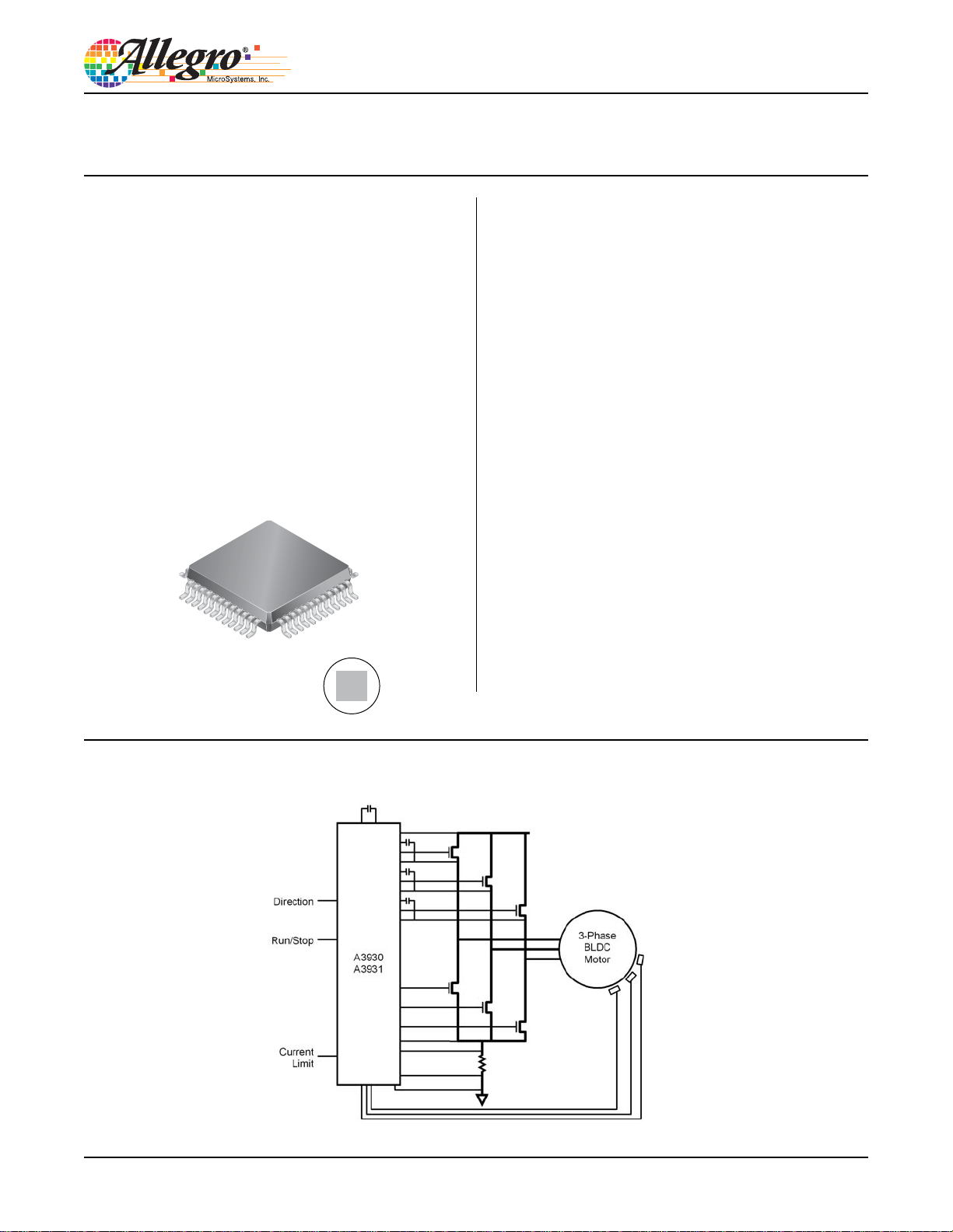
The A3930 and A3931 are 3-phase brushless DC (BLDC) motor
controllers for use with N-channel external power MOSFETs.
They incorporate much of the circuitry required to design a
cost effective three-phase motor drive system, and have been
specifically designed for automotive applications.
A key automotive requirement is functionality over a wide
input supply range. A unique charge pump regulator provides
adequate (>10 V) gate drive for battery voltages down to 7 V,
and allows the device to operate with a reduced gate drive at
battery voltages down to 5.5 V. Power dissipation in the charge
pump is minimized by switching from a voltage doubling mode
at low supply voltage to a dropout mode at the nominal running
voltage of 14 V.
A bootstrap capacitor is used to provide the above-battery
supply voltage required for N-channel MOSFETs. An internal
charge pump for the high-side drive allows for DC (100% duty
cycle) operation.
Internal fixed-frequency PWM current control circuitry can
be used to regulate the maximum load current. The peak
load current limit is set by the selection of an input reference
voltage and external sensing resistor. The PWM frequency is
set by a user-selected external RC timing network. For added
flexibility, the PWM input can be used to provide speed and
Approximate Scale 1:1
Continued on the next page…
T ypical Application
3930-DS Rev. 2

A3930 and
Automotive 3-Phase BLDC Controller
A3931
Description (continued)
torque control, allowing the internal current control circuit to set
the maximum current limit.
Efficiency is enhanced by using synchronous rectification. The
power FETs are protected from shoot-through by integrated
crossover control with dead time. The dead time can be set by a
single external resistor.
The A3930 and A3931 only differ in their response to the all-zero
Selection Guide
Part Number Option Packing Terminals Package
A3930KJP-T Hall short detection 250 pieces/tray
A3930KJPTR-T Hall short detection 1500 pieces/reel
A3931KJP-T Pre-positioning 250 pieces/tray
A3931KJPTR-T Pre-positioning 1500 pieces/reel
combination on the Hall inputs. In this state, the A3930 indicates
a logic fault, but the A3931 pre-positions the motor in an unstable
starting position suitable for start-up algorithms in microprocessordriven “sensor-less” control systems.
Both devices are supplied in a 48-pin LQFP with exposed thermal
pad. This is a small footprint (81 mm2) power package, that is lead
(Pb) free, with 100% matte tin leadframe plating.
48 LQFP surface mount
and MOSFET Driver
Absolute Maximum Ratings
Parameter Symbol Conditions Rating Units
Load Supply Voltage V
V
Logic Input/Output Voltage
Output Voltage Range
Operating Temperature Range (K) T
Junction Temperature T
Transient Junction Temperature T
Storage Temperature Range T
ESD Rating, Human Body Model
ESD Rating, Charged Device Model AEC-Q100-011, all pins 1050 V
RESET
V
V
V
V
VBB pin –0.3 to 50 V
BB
RESET pin input –0.3 to 6 V
Remaining logic pins –0.3 to 7 V
GHA, GHB, and GHC pins VSx to VSx+ 15 V
GHx
GLA, GLB, and GLC pins –5 to 16 V
GLx
CA, CB, and CC pins VSx+ 15 V
Cx
SA, SB, and SC pins –5 to 55 V
Sx
CSP, CSN, and LSS pins –4 to 6.5 V
CSO, VDSTH pins –0.3 to 6.5 V
VDRAIN pin –0.3 to 55 V
A
J
Overtemperature event not exceeding 1 s, lifetime duration not exceed-
tJ
ing 10 hr; guaranteed by design
characterization
S
AEC-Q100-002, all pins except CP1 2000 V
AEC-Q100-002, pin CP1 1000 V
–40 to 150 °C
–55 to 150 °C
150 °C
175 °C
Allegro MicroSystems, Inc.
115 Northeast Cutoff
Worcester, Massachusetts 01615-0036 U.S.A.
1.508.853.5000; www.allegromicro.com
2
A3930 and
Automotive 3-Phase BLDC Controller
A3931
QV5
VBAT+
V5BD
CV5
MODE
COAST
BRAKE
RESET
DIR
and MOSFET Driver
Functional Block Diagram
CP
VBB
V5
H1
+5V Ref
Control
Logic
Phase A of three phases
CP1CP2
Charge
Pump
Regulator
Charge
Pump
Boostrap
Monitor
High-Side
Drive
VREG
VDRAIN
CA
GHA
SA
CREG
CBOOTA
RGHA
P
V5
H1
H2
H3
&C
&B
H2
H3
RDEAD
PWM
TACHO
DIRO
ESF
FF1
FF2
Pad
Diagnostics and
Protection
–UVLO
–TSD
–Short to Supply
–Short to Ground
–Shorted Winding
–Low Load
VDSTH
RC
Q
OSC
VREG
Low-Side
Drive
R
Blanking
S
REF
CSOUT
CTRT
AGND
GLA
RGLA
LSS
TEST
CSP
CSN
P
&A
RSENSE
Allegro MicroSystems, Inc.
115 Northeast Cutoff
Worcester, Massachusetts 01615-0036 U.S.A.
1.508.853.5000; www.allegromicro.com
3

A3930 and
Automotive 3-Phase BLDC Controller
A3931
ELECTRICAL CHARACTERISTICS at T
Characteristics Symbol Test Conditions Min. Typ. Max. Units
Supply and Reference
VBB Functional Operating Range
VBB Quiescent Current
V5 Quiescent Current I
VREG Output Voltage V
Bootstrap Diode Forward Voltage V
Bootstrap Diode Resistance r
Bootstrap Diode Current Limit I
Top-off Charge Pump Current Limit I
High-Side Gate Drive Static Load
Resistance
V5 Output Voltage V
VBE of External Transistor QV5 V
V5BD Base Drive Capability for QV5
Gate Output Drive
Turn-On Rise Time t
Turn-Off Fall Time t
Pull-Up On Resistance R
Pull-Down On Resistance R
Short-Circuit Current – Source
Short-Circuit Current – Sink I
GHx Output Voltage V
GLx Output Voltage V
6
2
2
= –40°C to 150°C, V
J
DS(on)UP
DS(on)DN
I
SC(source)TJ
SC(sink)
V
BB
I
BBQ
I
BBS
V5Q
REG
fBOOT
D
DBOOT
TOCPM
R
GSH
5
BEEXT
I
5BD
r
f
GHx
GLx
and MOSFET Driver
= 7 to 45 V, unless otherwise noted
BB
Function correct, parameters not
guaranteed
RESET = High, outputs = Low – 11 14 mA
RESET = Low, sleep mode – – 10 A
RESET = High, outputs = Low – – 5 mA
V
7.4 V, I
BB
6 V < V
BB
I
= 0 to 15 mA
REG
5.5 V < VBB < 6 V, I
= 0 to 15 mA 12.10 13 13.75 V
REG
< 7.4 V
< 10 mA 9 10 – V
REG
ID = 10 mA 0.4 0.7 1.0 V
ID = 100 mA 1.5 2.2 2.8 V
r
D(100 mA)
V
C
LOAD
C
LOAD
TJ = 25°C, I
TJ = 150°C, I
TJ = 25°C, I
TJ = 150°C, I
= (V
fBOOT(150 mA)
fBOOT(50 mA)
–
) / 100 mA
= 3300 pF, 20% to 80% points – 60 – ns
= 3300 pF, 80% to 20% points – 40 – ns
= –150 mA 3 4 5
GHx
= –150 mA 4.6 5.6 6.6
GHx
= 150 mA 1 1.5 2
GLx
= 150 mA 1.5 2.3 3
GLx
= 25°C – –500 – mA
TJ = 25°C – 850 – mA
tw < 10 s
Bootstrap capacitor fully charged
1
5.5 – 50 V
2 × V
BB
–2.7
––V
61020
250 500 750 mA
– 200 – A
250 – – k
4.75 5 5.25 V
––1V
– – –2 mA
V
– 0.2 – – V
Cx
V
–
REG
0.2
––V
Continued on the next page...
Allegro MicroSystems, Inc.
115 Northeast Cutoff
Worcester, Massachusetts 01615-0036 U.S.A.
1.508.853.5000; www.allegromicro.com
4

A3930 and
Automotive 3-Phase BLDC Controller
A3931
ELECTRICAL CHARACTERISTICS (continued) at T
Characteristics Symbol Test Conditions Min. Typ. Max. Units
Turn-Off Propagation Delay t
Dead Time (turn-off to turn-on delay) t
Logic Inputs and Outputs
FFx Fault Output (Open Drain) V
FFx Fault Output Leakage Current
2
TACHO and DIRO Output High Voltage V
TACHO and DIRO Output Low Voltage V
Input Low Voltage V
Input High Voltage (Except RESET) V
RESET Input High Voltage V
Input Hysteresis V
Input Current (Except H1, H2, H3, and
RESET)
2
RESET Input Pull-Down Resistor R
Hx Input Pull-Up Resistor R
Current Sense Differential Amplifier
Input Bias Current
Input Offset Current
2
2
CSP Input Resistance R
CSN Input Resistance R
Differential Input Voltage V
Output Offset Voltage V
Output Offset Voltage Drift V
Input Common Mode Range V
Differential Input Voltage Gain A
Low Output Voltage Error V
DC Common Mode Gain A
Source Resistance r
Output Dynamic Range V
Output Current – Sink I
Output Current – Source
2
p(off)
DEAD
OL
I
OH
OH
OL
IL
IH
IHR
IHys
I
IN
PD
PU
I
IBS
I
IOS
CSP
CSN
ID
OOS
OOS(t)
CM
V
err
CMdc
CSOUT
CSOUT
CSOUT(sink)VCSOUT
I
CSOUT(source)VCSOUT
and MOSFET Driver
= –40°C to 150°C, V
J
From Hall input change to unloaded
gate output change
From other control input change to
unloaded gate output change
R
= 5 k – 180 – ns
DEAD
R
= 50 k 835 960 1090 ns
DEAD
R
= 400 k – 3.3 – s
DEAD
= 7 to 45 V, unless otherwise noted
BB
300 500 700 ns
– 150 200 ns
RDEAD = tied to V5 – 6 – s
I
= 1 mA, fault asserted – – 0.4 V
OL
VO = 5 V, fault not asserted –1 – 1 A
I
= –1 mA V5 – 1 V – – V
OH
I
= 1 mA – – 0.4 V
OL
– – 0.8 V
2––V
2.2 – – V
300 500 – mV
–1 – 1 A
V
= 5 V – 50 – k
IN
V
= 0 V – 100 – k
IN
CSP = CSN = 0 V –250 –200 –150 A
CSP = CSN = 0 V –10 – 10 A
Measured with respect to AGND – 80 – k
Measured with respect to AGND – 4 – k
V
= CSP – CSN, –1.3 V < CSP < 4 V,
ID
–1.3 V < CSN < 4 V
0 – 200 mV
CSP = CSN = 0 V 100 320 550 mV
CSP = CSN = 0 V – 100 – V/°C
CSP = CSN –1.5 – 4 V
40 mV < V
0 < V
V
CSOUT
< 175 mV, VCM in range 18.5 19 19.5 V/V
ID
< 40 mV,
ID
= (19 × VID) + V
OOS
+ V
err
–20 – 20 mV
CSP = CSN = 200 mV – –30 – dB
V
–100 A < I
= 2 V, –2 mA < I
CSOUT
< 0.5 mA – 80 –
CSOUT
< 100 A 0.1 –
CSOUT
= 2 V ±5% – 1 – mA
= 2 V ±5% – –19 – mA
1
– 0.2
V5
V
Continued on the next page…
Allegro MicroSystems, Inc.
115 Northeast Cutoff
Worcester, Massachusetts 01615-0036 U.S.A.
1.508.853.5000; www.allegromicro.com
5

A3930 and
Automotive 3-Phase BLDC Controller
A3931
ELECTRICAL CHARACTERISTICS (continued) at T
= –40°C to 150°C, V
J
= 7 to 45 V, unless otherwise noted
BB
and MOSFET Driver
1
Characteristics Symbol Test Conditions Min. Typ. Max. Units
Supply Rejection PSRR CSP = CSN = AGND, 0 to 300 kHz – 45 – dB
Small Signal 3 dB Bandwidth Frequency f
Settling Time t
AC Common Mode Gain A
Common Mode Recovery Time t
3dB
SETTLE
CMac
CMrec
Output Slew Rate SR
Input Overload Recovery Time t
IDREC
VID=10 mV
To within 10%, V
PP
= 1 VPP square
CSOUT
wave
V
= 250 mVPP, 0 to 1 MHz – –28 – dB
ICR
To within 100 mV, V
= +4.1 to 0 V
ICR
step
10% to 90% points, VID= 0 to 175 mV
step
– 1.6 – MHz
– 400 – ns
–1–s
–20–V/s
To within 10%, VID=250 mV to 0 V step – 500 – ns
Current Limit
Reference Comparator Input Offset Voltage V
Reference Input Clamp Voltage V
Comparator Blank Time t
REF Input Bias Current I
RC Charge Current
2
RC HIgh Voltage Threshold V
RC Low Voltage Threshold V
IOC
REFC
RC
IBREF
I
RC
RCH
RCL
External pull-up to 5 V R
= 200 k 3.75 4 4.2 V
REF
RT= 56 k, CT = 470 pF – 650 – ns
–15 0 15 mV
–0–A
–1.15 –1 –0.85 mA
1.7 1.9 2.1 V
0.6 0.7 0.8 V
Protection
V
rising 7.5 8 8.5 V
VREG Undervoltage Lockout V
Bootstrap Capacitor Undervoltage Lockout V
Bootstrap Capacitor Undervoltage Lockout
Hysteresis
V5 Undervoltage Lockout V
V5 Undervoltage Lockout Hysteresis V
VDSTH Input Voltage Range V
VDSTH Input Current
2
VDRAIN Input Voltage Range V
Short-to-Ground Threshold Offset
Short-to-Battery Threshold Offset
3,5
4,5
Low Load Current Detection Voltage V
Overtemperature Flag T
Overtemperature Flag Hysteresis T
1
Parameters are tested at 135°C. Values at 150°C are guaranteed by design or correlation.
2
For input and output current specifications, negative current is defined as coming out of (sourcing) the specified device pin.
3
High side on. As VSX decreases, fault occurs if V
4
Low side on. As VSX increases, fault occurs if V
5
V
threshold is V
STG
6
Function is correct but parameters not guaranteed above or below general limits (7 to 45 V).
DTSTH
+ V
STGO
. V
STB
threshold is V
REGUV
BOOTUVVBOOT
V
BOOTUVHysVBOOTUVHys
5UV
5UVHys
DSTH
I
DSTH
DRAIN
V
STGO
V
STBO
CSOL
JF
JFHys
– V
– V
SX
LSS
DTSTH
> V
> V
BAT
SX
REG
V
falling 6.75 7.25 7.75 V
REG
falling, VCx – V
= %V
REG
Sx
59 – 69 %
–13–%
V5 falling 3.4 3.65 4.0 V
300 400 500 mV
0.3 – 4 V
–1 – 1 A
7VBB45 V
V
> 1 V – ±300 – mV
DSTH
V
1 V, 7 V V
DSTH
V
> 1 V – ±300 – mV
DSTH
V
1 V, 7 V V
DSTH
30 V –150 – 150 mV
DRAIN
30 V –150 – 150 mV
DRAIN
– 500 – mV
Temperature increasing – 170 – ºC
Recovery = T
.
STG
.
STB
+ V
STBO
.
JF
– T
JFHys
–15–ºC
Allegro MicroSystems, Inc.
115 Northeast Cutoff
Worcester, Massachusetts 01615-0036 U.S.A.
1.508.853.5000; www.allegromicro.com
6

A3930 and
Automotive 3-Phase BLDC Controller
A3931
and MOSFET Driver
Thermal Characteristics
THERMAL CHARACTERISTICS may require derating at maximum conditions, see Applications Information section
Characteristic Symbol Test Conditions* Value Units
4-layer PCB, based on JEDEC standard 23 ºC/W
Package Thermal Resistance R
Die-to-Exposed Pad Thermal Resistance
*Additional thermal information available on Allegro Web site.
JA
R
JP
Power Dissipation versus Ambient Temperature
2-layer PCB, with 3 in.
by thermal vias
2
of copper area each side connected
44 ºC/W
2 ºC/W
6.0
5.0
4.0
R
R
QJA
Q
JA
= 23°C/W
= 44°C/W
3.0
2.0
1.0
0
ALLOWABLE PACKAGE POWER DISSIPATION IN WATTS
50 75 100 125 15025
AMBIENT TEMPERATURE IN °C
Allegro MicroSystems, Inc.
115 Northeast Cutoff
Worcester, Massachusetts 01615-0036 U.S.A.
1.508.853.5000; www.allegromicro.com
7

A3930 and
Automotive 3-Phase BLDC Controller
A3931
Functional Description
Basic Operation
The A3930 and A3931 devices provide commutation and current
control for 3-phase brushless DC (BLDC) motors with integrated
Hall-effect (HE) sensors. The motor current is provided by an
external 3-phase N-channel MOSFET bridge which is controlled
by the A3930/A3931, using fixed-frequency pulse width modulation (PWM). The use of PWM with N-channel MOSFETs
provides the most cost-effective solution for a high-efficiency
motor drive.
The A3930/A3931 provides all the necessary circuits to ensure
that the gate-source voltage of both high-side and low-side external MOSFETs are above 10 V, at supply voltages down to 7 V.
For extreme battery voltage drop conditions, functional operation
is guaranteed down to 5.5 V but with a reduced gate drive. The
A3930/A3931 also decodes the commutation sequence from three
HE sensors spaced at 120° in the electrical cycle, and ensure no
cross-conduction (shoot through) in the external bridge. Individual pins provide direction, brake and coast control.
Motor current can be sensed by a low-value sense resistor,
RSENSE, in the ground connection to the bridge, amplified and
compared to a reference value. The A3930/A3931 then limits the
bridge current on a cycle-by-cycle basis. Bridge current can also
be controlled using an external PWM signal with the internal current control either disabled or used to set the absolute maximum
motor current. Specific functions are described more fully in the
following sections.
Power Supplies
Only one power connection is required because all internal
circuits are powered by integrated regulators. The main power
supply should be connected to VBB through a reverse battery
protection circuit.
V5 and V5BD A 5 V supply for external pull-up and bias cur-
rents is provided by an integrated 5 V regulator controller and an
external NPN transistor, QV5. The A3930/A3931 provides the
base drive current on the V5BD pin, and the 5 V reference on the
V5 pin. This regulator is also used by the internal logic circuits
and must always be decoupled by at least a 200 nF capacitor,
CV5, between the V5 pin and AGND. For stability, a 100 nF
capacitor, C5BD, also should be connected between V5BD and
and MOSFET Driver
AGND. If an external 5 V supply is not required, the V5BD pin
and the V5 pin should be connected together.
CP1, CP2, and VREG The gate drive outputs are powered by
an internal charge pump, which requires a pump capacitor, typically 470 nF, CP, connected between the CP1 and CP2 pins. The
output from the charge pump, 13 V nominal, is used to power
each of the three high- and low-side driver pairs and is also
available on the VREG pin. A sufficiently large storage capacitor, CREG, must be connected to this pin to provide the transient charging current to the low-side drivers. The charge pump
also provides the charging current for the bootstrap capacitors,
CBOOTx.
An additional “top-off” charge pump is provided for each highside drive which allows the high-side drive to maintain the gate
voltage on the external FET indefinitely, ensuring so-called 100%
PWM if required. This is a low-current trickle charge pump
(< 100 A typical), and is only operated after a high-side driver
has been signaled to turn on. There is a small amount of bias
current (< 20 A) drawn from the Cx pin to operate the floating
high-side circuit, and the charge pump simply provides enough
drive to ensure that the bootstrap voltage, and hence the gate voltage, will not droop due to this bias current. The charge required
for initial turn-on of the high-side gate is always supplied by
bootstrap capacitor charge cycles.
Hall Effect Sensor Inputs
H1, H2, and H3 Hall-effect sensor inputs are configured for
motors with 120° electrically-spaced HE sensors, but may be
used for 60° electrical spacing with an external inverter. HE sensors usually require an additional pull-up resistor to be connected
between the sensor output and 5 V. This 5 V can be provided by
the integrated 5 V regulator. HE inputs have a hysteresis of typically 500 mV to reduce the effects of switching noise on the HE
connections to the motor. These inputs are also filtered to further
reduce the effects of switching noise. The HE inputs are pulledup to 5 V inside the A3930/A3931 through a high value (100
k typical) resistor in series with a diode. This internal pull-up
makes the HE input appear high if the Hall sensor signal is missing, allowing detection of an HE input logic fault.
Allegro MicroSystems, Inc.
115 Northeast Cutoff
Worcester, Massachusetts 01615-0036 U.S.A.
1.508.853.5000; www.allegromicro.com
8

A3930 and
Automotive 3-Phase BLDC Controller
A3931
In order to provide a known start-up position for the motor, an
optional prepositioning function is available in the A3931. When
the Hall inputs are all driven low (H1 = H2 = H3 = 0), the power
FETs in the A phase source current from the supply, and those in
both the B and C phases sink current. This forces the motor to
move to an unstable position midway between two detent points
and allows any start-up algorithm to ensure correct initial direction of rotation. Note that this is only available in the A3931. The
A3930 will indicate a logic fault when all Hall inputs are driven
low. The commutation truth table for these inputs is shown in
table 2. The inputs can also be driven directly from a microcontroller or similar external circuit.
Gate Drive
The A3930/A3931 is designed to drive external N-channel power
MOSFETs. They supply the large transient currents necessary to
quickly charge and discharge the gate capacitance of the external
FETs in order to reduce dissipation in the external FETs during
switching. The charge and discharge rate can be controlled using
external resistors in series with the connections to the gate of the
FETs.
RDEAD Cross-conduction is prevented by the gate drive circuits
which introduce a dead time, t
off and the complementary FET on. The dead time is derived
from the value of a resistor, RDEAD, connected between the
RDEAD pin and AGND. If RDEAD is connected to V5, t
defaults to 6 s typical.
GLA, GLB, and GLC Low-side gate drive outputs for external
NMOS drivers. External series-gate resistors, RGATE, (as close
as possible to the NMOS gate) can be used to control the slew
rate seen at the power-driver gate, thereby controlling the di/dt
and dv/dt of the Sx outputs. Referring to table 2, GLx = 1 (high)
means that the upper half (PMOS) of the driver is turned on, and
that its drain will source current to the gate of the low-side FET
in the external motor-driving bridge. GLx = 0 (low) means that
the lower half (NMOS) of the driver is turned on, and that its
drain will sink current from the corresponding external FET gate
circuit to the LSS pin.
, between switching one FET
DEAD
DEAD
and MOSFET Driver
which should have low-impedance traces to the FET bridge.
GHA, GHB, and GHC High-side gate drive outputs for exter-
nal NMOS drivers. External series-gate resistors, RGATE, can
be used to control the slew rate seen at the power-driver gate,
thereby controlling the di/dt and dv/dt of the Sx inputs. Referring
to table 2, GHx = 1 (high) means that the upper half (PMOS) of
the driver is turned on, and that its drain will source current to the
gate of the high-side FET in the external motor-driving bridge.
GHx = 0 (low) means that the lower half (NMOS) of the driver
is turned on, and that its drain will sink current from the corre-
sponding external FET gate circuit to the respective Sx pin.
CA, CB, and CC High-side connections for the bootstrap
capacitors and positive supply for high-side gate drivers. The
bootstrap capacitors, CBOOTx, are charged to approximately
V
when the corresponding Sx terminal is low. When the Sx
REG
output swings high, the voltage on the Cx pin rises with the out-
put to provide the boosted gate voltage needed for the high-side
N-channel power MOSFETs.
VDRAIN High impedance sense input (Kelvin connection) to
the top of the external FET bridge. This input allows accurate
measurement of the voltage at the drain of the high-side FETs and
should be connected directly to the bridge, close to the drain connections of the high-side FETs, with an independent trace.
LSS Low-side return path for discharge of the gate capacitors.
It is connected to the common sources of the low-side external
FETs through an independent low-impedance trace.
Logic Control Inputs
Additional logic-level inputs are provided to enable specific
features described below. These logic inputs all have a nominal
hysteresis of 500 mV to improve noise performance.
RESET Allows minimum current consumption from the VBB
supply. When RESET is low, all internal circuitry is disabled
including the V5 output. When coming out of sleep state, the
protection logic ensures that the gate drive outputs are off until
the charge pump reaches proper operating conditions. The charge
pump stabilizes in approximately 3 ms under nominal conditions.
SA, SB, and SC Directly connected to the motor, these
terminals sense the voltages switched across the load. These
terminals are also connected to the negative side of the bootstrap
capacitors and are the negative supply connections for the
floating high-side drivers. The discharge current from the highside FET gate capacitance flows through these connections,
RESET has an internal pull-down resistor, 50 k typical.
However, to allow the A3930/A3931 to start-up without the
need for an external logic input, the RESET pin can be pulled
to the battery voltage with an external pull-up resistor. Because
RESET also has an internal clamp diode, 6 V typical, to limit the
input current, the value of the external pull-up resistor should be
Allegro MicroSystems, Inc.
115 Northeast Cutoff
Worcester, Massachusetts 01615-0036 U.S.A.
1.508.853.5000; www.allegromicro.com
9

A3930 and
Automotive 3-Phase BLDC Controller
A3931
greater than 20 k. The upper limit for the resistor must be low
enough to ensure that the input voltage reaches the input high
threshold, V
COAST An active-low input which turns all FETs off without
disabling the supplies or control logic. This allows the external
FETs and the motor to be protected in case of a short circuit.
MODE Sets the current-decay method. Referring to table 3, when
in slow-decay mode, MODE = 1, only the high-side MOSFET
is switched off during a PWM-off cycle. In the fast-decay mode,
MODE = 0, the device switches both the high-side and low-side
MOSFETs.
Slow decay allows a lower ripple current in the motor at the
PWM frequency, but reduces the dynamic response of the current control. It is suitable for motors which run at a more-or-less
constant speed. Fast decay provides improved current-control
dynamic response, but increases the motor current ripple. It is
suitable for motors used in start-stop and positioning applications.
DIR Determines the direction of motor torque output, as shown in
table 2. For an unloaded, low-inertia motor, this will also usually
be the direction of mechanical rotation. With a motor that has a
high inertial load, the DIR input can be used to apply a controlled
breaking torque, when fast decay is used (MODE = 0).
BRAKE An active-low input that provides a braking function.
When BRAKE = 0 (see table 3), all the low-side FETs are turned
on and the high-side FETs are turned off. This effectively shortcircuits the back EMF in the windings, and brakes the motor.
The braking torque applied depends on the speed. RESET = 0 or
COAST = 0 overrides BRAKE and coasts the motor. Note that
when BRAKE is used to dynamically brake the motor, the windings are shorted with no control over the winding current.
ESF The state of the enable stop on fault (ESF) pin determines
the action taken when a short is detected. See the Diagnostics
section for details.
TEST Test is for Allegro production use and must be connected
to AGND.
Current Regulation
Load current can be regulated by an internal fixed frequency
PWM control circuit or by external input on the PWM pin.
Current Sense Amplifier: CSP, CSN, and CSOUT A dif-
ferential current sense amplifier with a gain, A
provided to allow the use of low-value sense resistors or current
shunts as the current sensing elements. Because the output of
this sense amplifier is available at CSOUT, it can be used for
either internal or external current sensing. With the sense resistor,
INR
.
, of 19 typical, is
V
and MOSFET Driver
RSENSE, connected between CSP and CSN, the output of the
sense amplifier will be approximately:
× A
OOS
) .
V
) .
,
CSOUT
V
where V
is the output offset voltage (the voltage at zero load
OOS
current), and A
(I
CSOUT
is the differential voltage gain of the sense
V
LOAD
× AV × R
SENSE
) + V
amplifier, 19 typical.
Internal Current Control: REF A fixed reference voltage
can be applied to provide a maximum current limit. A variable
reference voltage will provide a variable torque control. The
output voltage of the current sense differential amplifier, V
is compared to the reference voltage available on the REF
pin. When the outputs of the MOSFETs are turned on, current
increases in the motor winding until it reaches a trip point value,
I
, given by:
TRIP
I
TRIP
= (V
REF
– V
OOS
) / (R
SENSE
At the trip point, the sense comparator resets the source enable
latch, turning off the source driver. At this point, load inductance
causes the current to recirculate until the start of the next PWM
period.
The current path during recirculation is determined by the
configuration of the MODE pin. Torque control can therefore be
implemented by varying the voltage on the REF pin, provided
that the PWM input remains high. If direct control of the torque
or current by PWM input is desired, a voltage can be applied to
the REF pin to set an absolute maximum current limit. The REF
input is internally limited to 4 V, which allows the use of a simple
pull-up resistor to V5, RREF, to set the maximum reference
voltage, avoiding the need for an externally generated reference
voltage. RREF should have a value between 20 k and 200 k.
Internal PWM Frequency The internal oscillator frequency,
, is determined by an external resistor, RT, and capacitor, CT,
f
OSC
connected in parallel from the RC pin to AGND. The frequency
is approximately:
where f
1 / (RTCT + t
f
OSC
in the range 20 to 50 kHz.
OSC
BLANK
+ t
DEAD
PWM Input Can be used to control the motor torque by an exter-
nal control circuit signal on the PWM pin. Referring to table 3,
when PWM = 0, the selected drivers are turned off and the load
inductance causes the current to recirculate. The current path during recirculation is determined by the configuration of the MODE
pin. Setting PWM = 1 will turn on selected drivers as determined
by the Hx input logic. Holding PWM=1 allows speed and torque
control solely by the internal current-limit circuit, using the voltage on the REF pin.
,
Allegro MicroSystems, Inc.
115 Northeast Cutoff
Worcester, Massachusetts 01615-0036 U.S.A.
1.508.853.5000; www.allegromicro.com
10

A3930 and
Automotive 3-Phase BLDC Controller
A3931
In some circumstances, it may be desirable to completely disable
the internal PWM control. This can be done by pulling the RC
pin directly to AGND. This will disable the internal PWM oscillator and ensure that the output of the PWM latch is always high.
Blank Time When the source driver is turned on, a current spike
occurs due to the reverse-recovery currents of the clamp diodes
and switching transients related to distributed capacitance in the
load. To prevent this current spike from erroneously resetting
the source enable latch, the current-control comparator output
is blanked for a short period of time, t
driver is turned on.
The length of t
is different for internal versus external
BLANK
PWM. It is set by the value of the timing capacitor, CT, according
to the following formulas:
for internal PWM: t
for external PWM: t
A nominal C
value of 680 pF yields a t
T
(s) = 1260 × C
BLANK
(s) = 2000 × C
BLANK
external PWM, and 860 ns for internal PWM. The user must
ensure that CT is large enough to cover the current spike duration
when using the internal sense amplifier.
Diagnostics
Several diagnostic features integrated into the A3930/A3931
provide speed and direction feedback and indications of fault
conditions.
TACHO and DIRO These outputs provide speed and direction
information based on the HE inputs from the motor. As shown in
figure 1, at each commutation point, the TACHO output changes
state independent of motor direction. The DIRO output is updated
at each commutation point to show the motor direction. When
the motor is rotating in the “forward” or positive direction, DIRO
will be high. When rotation is in the “reverse” or negative direction, DIRO will be low. The actual direction of rotation is deter-
mined from the sequence of the three Hall inputs, Hx. Forward
is when the sequence follows table 2 top-to-bottom and reverse
when the sequence follows table 2 bottom-to-top.
DIRO
TACHO
Commutation
Points
"Forward" Motor Rotation "Reverse" Motor Rotation
Figure 1. Direction Indication Outputs
, when the source
BLANK
(F), and
T
(F) .
T
of 1.3 s for
BLANK
and MOSFET Driver
Note that there are some circumstances in which the direction
reported on the DIRO output pin and the direction demanded
on the DIR input pin may not be the same. This may happen if
the motor and load have reasonably high inertia. In this case,
changing the state of the DIR pin will cause the torque to reverse,
braking the motor. During this braking, the direction indicated on
the DIRO output will not change.
ESF The state of the enable stop on fault (ESF) pin will deter-
mine the action taken when a short is detected. For other fault
conditions, the action is defined by the type of fault. The action
taken follows the states shown in table 1.
When ESF = 1, any short fault condition will disable all the
gate drive outputs and coast the motor. This disabled state will
be latched until the next phase commutation or until COAST or
RESET go low.
When ESF = 0, under most conditions, although the fault flags,
FF1 and FF2, are still activated, the A3930/A3931will not disrupt
normal operation and will therefore not protect the motor or the
drive circuit from damage. It is imperative that the master control
circuit or an external circuit take any necessary action when a
fault occurs, to prevent damage to components.
If desired, the active low COAST input can be used as a crude
disable circuit by connecting the fault flags FF1 and FF2 to the
COAST input and a pull-up resistor to V5.
FF1, FF2, and VDSTH Fault conditions are indicated by the
state of two open drain output fault flags, FF1 and FF2, as shown
in table 1. In addition to internal temperature, voltage, and logic
monitoring, the A3930/A3931 monitors the state of the external
MOSFETs and the motor current to determine if short circuit
faults occur or a low load condition exists. In the event that two
or more faults are detected simultaneously, the state of the fault
flags will be determined by a logical AND of the fault states of
each flag.
• Undervoltage VREG supplies the low-side gate driver and the
bootstrap charge current. It is critical to ensure that the voltages
are sufficiently high before enabling any of the outputs. The
undervoltage circuit is active during power-up, and will pull
both fault flags low and coast the motor (all gate drives low)
until V
sufficient to turn on the external power FETs at a battery voltage
as low as 5.5 V, but will not normally provide the rated on-resistance of the FET. This could lead to excessive power dissipation
in the external FET.
is greater than approximately 8 V. Note that this is
REG
Allegro MicroSystems, Inc.
115 Northeast Cutoff
Worcester, Massachusetts 01615-0036 U.S.A.
1.508.853.5000; www.allegromicro.com
11

A3930 and
Automotive 3-Phase BLDC Controller
A3931
In addition to a monitor on VREG, the A3930/A3931 also
monitors both the bootstrap charge voltage, to ensure sufficient
high-side drive, and the 5 V reference voltage at V5, to ensure
correct logical operation. If either of these fall below the lockout voltage level, the fault flags are set.
• Overtemperature This event pulls both fault flags low but
does not disable any circuitry. It is left to the user to turn off
the device to prevent overtemperature damage to the chip and
unpredictable device operation.
• Logic Fault: Hall Invalid The A3930 and the A3931 differ
slightly in how they handle error conditions on the Hall inputs,
Hx. When all Hx are 1s, both devices evaluate this as an illegal
code, and they pull both fault flags, FFx, low and coast the mo-
tor. This action can be used, if desired, to disable all FET drives
under bridge or motor fault conditions. The Hall logic fault
condition is not latched, so if the fault occurs while the motor is
running, the external FETs will be reenabled, according to the
commutation truth table (table 2), when the Hx inputs become
valid.
When all Hx are 0s, the A3930 handles this in the same manner
as all 1s, described in the preceding paragraph. The A3931,
however, evaluates this as a prepositioning code, and does not
register it as a fault.
The Hx inputs have pull-up resistors to ensure that a fault condi-
tion will be indicated in the event of an open connection to a
Hall sensor.
• Short to Ground A short from any of the motor phase con-
nections to ground is detected by monitoring the voltage across
the top FETs in each phase using the appropriate Sx pin and the
voltage at VDRAIN. This drain-source voltage is then compared
to the voltage on the VDSTH pin. If the drain source voltage
exceeds the voltage at the VDSTH pin, FF2 will be pulled low.
• Short to Supply A short from any of the motor phase connec-
tions to the battery or VBB connection is detected by monitoring the voltage across the bottom FETs in each phase using the
appropriate Sx pin and the LSS pin. This drain-source voltage
is then compared to the voltage on the VDSTH pin. If the drain
source voltage exceeds the voltage at the VDSTH pin, FF2 will
be pulled low.
• Shorted Motor Winding A short across the motor phase
winding is detected by monitoring the voltage across both the
top and bottom FETs in each phase. This fault will pull FF2 low.
• Low Load Current The sense amplifier output is monitored
independently to allow detection of a low load current. This can
and MOSFET Driver
be used to detect if an open load condition is present. If, during
a commutation period, the output from the sense amplifier does
not go above a minimum value, V
further action will be taken.
Short Fault Operation Because motor capacitance may cause
the measured voltages to show a fault as the phase switches, the
voltages are not sampled until one t
nal FET is turned on.
If a short circuit fault occurs when ESF = 0, the external FETs
are not disabled by the A3930/A3931. Under some conditions,
some measure of protection will be provided by the internal current limit but in many cases, particularly for a short to ground,
the current limit will provide no protection for the external
FETs. To limit any damage to the external FETs or the motor, the
A3930/A3931 can either be fully disabled by the RESET input
or all FETs can be switched off by pulling the COAST input low.
Alternatively, setting ESF = 1 will allow the A3930/A3931 to disable the outputs as soon as the fault is detected. The fault will be
latched until any of the following conditions occur:
• a phase commutation
• RESET goes low
• COAST goes low
This will allow a running motor to coast to the next phase
commutation without the risk of damage to the external power
MOSFETs.
Low Load Current Fault Operation No action is taken for
a low load current condition. If the low load occurs due to an
open circuit on a phase connection while the motor is running,
the A3930/A3931 will continue to commutate the motor phases
according to the commutation truth table, table 2.
In some cases, this will allow the motor to continue operating at
a much reduced performance. The low load condition is checked
during a commutation period and is only flagged at the next commutation event. The flag is cleared at the end of any subsequentcommutation period where no low load current fault is detected.
If the motor stalls or is stationary, then the remaining phase connections will usually be insufficient to start rotating the motor. At
start-up or after a reset, the low load condition is flagged until the
first time the motor current exceeds the threshold value, V
This allows detection of a possible open phase from startup, even
if the motor is not able to start running.
Note that a low load current condition can also exist if the motor
being driven has no mechanical load.
, FF1 will go low. No
CSOL
interval after the exter-
DEAD
CSOL
.
Allegro MicroSystems, Inc.
115 Northeast Cutoff
Worcester, Massachusetts 01615-0036 U.S.A.
1.508.853.5000; www.allegromicro.com
12

A3930 and
Automotive 3-Phase BLDC Controller
A3931
and MOSFET Driver
Table 1. Fault Action Table
FF1 FF2 Fault
0 0 Undervoltage Disable Disable
0 0 Overtemperature No Action No Action
0 0 Logic Fault Disable Disable
1 0 Short to ground No Action Disable
1 0 Short to supply No Action Disable
1 0 Shorted motor winding No Action Disable
0 1 Low load current No Action No Action
1 1 None No Action No Action
*Disable indicates that all gate outputs are low and all MOSFETs are
turned off.
Action*
ESF = 0 ESF = 1
Table 2. Commutation Truth Table*
Device H1 H2 H3 DIR GLA GLB GLC GHA GHB GHC SA SB SC
Both 1 0 1 1001100High Z Low
Both 1 0 0 1001010ZHigh Low
Both 1 1 0 1100010LowHigh Z
Both 0 1 0 1100001LowZHigh
Both 0 1 1 1010001ZLowHigh
Both 0 0 1 1010100High Low Z
A3930 0 0 0 X 0 0 0 0 0 0 Z Z Z
A3931 0 0 0 X 0 1 1 1 0 0 High Low Low
Both 1 1 1 X 0 0 0 0 0 0 Z Z Z
Both 1 0 1 0100001LowZHigh
Both 1 0 0 0010001ZLowHigh
Both 1 1 0 0010100High Low Z
Both 0 1 0 0001100High Z Low
Both 0 1 1 0001010ZHigh Low
Both 0 0 1 0100010LowHigh Z
*X indicates “don’t care,” Z indicates high impedance state
Table 3. INPUT LOGIC
MODE PWM BRAKE COAST RESET Decay Mode of Operation
00111Fast PWM chop – current decay with opposite of selected drivers ON
01111Fast Peak current limit – selected drivers ON
10111Slow PWM chop – current decay with both low-side drivers ON
11111Slow Peak current limit – selected drivers ON
X X 0 1 1 n/a Brake mode - All low-side gates ON
X X X 0 1 X Coast mode - All gates OFF
XXXX0XSleep mode – All gates OFF, low power state, 5 V OFF
*X indicates “don’t care”
Allegro MicroSystems, Inc.
115 Northeast Cutoff
Worcester, Massachusetts 01615-0036 U.S.A.
1.508.853.5000; www.allegromicro.com
13

A3930 and
Automotive 3-Phase BLDC Controller
A3931
Applications Information
Power
All supply connections to the A3930/A3931 should have capacitors mounted between the supply pins and the ground pin. These
capacitors will provide the transient currents which occur during
switching and decouple any voltage transients on the pin from the
main supply.
VBB Decouple with at least a 100 nF ceramic capacitor mounted
between the VBB pin and the AGND pin. A larger electrolytic
capacitor, typically 10 F, in parallel with the ceramic capacitor
is also recommended.
VREG Supplies current for the gate-drive circuit. As the gates
are driven high, they require current from an external capacitor
connected to VREG to support the transients. This capacitor
should be placed as close as possible to the VREG pin with the
ground connection close to the AGND pin. Its value should be at
least 20 times larger than the bootstrap capacitor. The capacitor
should have a very low series resistance (ESR) and inductance
(ESL) to avoid large voltage drops during the initial transient.
The optimum capacitor type is a high quality ceramic such as
X7R. However, when the required capacitance is too large, an
aluminium electrolytic capacitor may be used, with a smaller
ceramic capacitor (100 nF) in parallel.
V5 When the 5V regulator is used with an external pass transistor
to provide power to other circuits, a 10 F decoupling capacitor
should be connected between the V5 pin and AGND as close to
the pins as possible. If an electrolytic capacitor is used, then a
100 nF ceramic capacitor should be added in parallel. To improve
stability, a 100 nF capacitor also should be connected between
the V5BD pin and AGND. If 5V is not required for external
circuits, the external pass transistor may be omitted, but in that
case, V5 must connected directly to V5BD and decoupled with at
least a 220 nF capacitor between V5 and AGND.
AGND The A3930/A3931 has a single ground connection at the
AGND pin. The design ensures that only the operating current
for the controller stage passes through this pin. The charge and
discharge current for the external FETs does not pass though this
pin. The AGND pin is the ground reference for the current trip
threshold, the V
It should therefor be kept as quiet as possible. A suggested ground
connection scheme is described in the layout section below.
monitor threshold, and the timing components.
DS
and MOSFET Driver
Power Dissipation In applications where a high ambient tem-
perature is expected the on-chip power dissipation may become
a critical factor. Careful attention should be paid to ensure the
operating conditions allow the A3930/A3931 to remain in a safe
range of junction temperature.
The power consumed, P
mated using the following formulas:
P
P
where I
P
where V
P
where V
IAV = Q
P
SWITCHING
= P
TOT
BIAS
is 3 mA, typical, and
BB
CPUMP
< 15 V, or
BB
CPUMP
> 15 V, and
BB
BIAS
= VBB × I
= (2 × VBB–V
= (VBB–V
GATE
= Q
GATE
where N = 2 for slow decay, or N = 4 for fast decay, and
Ratio = 10 / (R
Bootstrap Capacitors
Bootstrap Capacitor Selection The value for C
be correctly selected to ensure proper operation of the device. If
the value is too large, time will be wasted charging the capacitor,
resulting in a limit on the maximum duty cycle and PWM
frequency. If the value is too small, there can be a large voltage
drop at the time when the charge is transferred from C
MOSFET gate.
To keep the voltage drop small, Q
a reasonable value. To calculate C
can be used:
Q
= Q
therefore
C
The voltage drop on the Cx pin as the MOSFET is being turned
on can be approximated by:
V = Q
Bootstrap Charging It is good practice to ensure that the high-
side bootstrap capacitor, CBOOT, is completely charged before a
BOOT
BOOT
= C
= Q
BOOT
GATE
GATE
GATE
, by the A3930/A3931 can be esti-
TOT
+ P
BB
REG
× N × f
× V
GATE
× V
CPUMP
,
REG
) × I
PWM
REG
+ 10)
BOOT
+ P
SWITCHING
) × I
AV
AV
,
× N × f
BOOT
BOOT
× Ratio
PWM
Q
GATE
, the following formulas
,
,
. A factor of 20 is
× 20,
× 20 / V
/ C
BOOT
BOOT
BOOT
BOOT
must
to the
Allegro MicroSystems, Inc.
115 Northeast Cutoff
Worcester, Massachusetts 01615-0036 U.S.A.
1.508.853.5000; www.allegromicro.com
14

A3930 and
Automotive 3-Phase BLDC Controller
A3931
high-side PWM cycle is requested. The minimum time required
to charge the capacitor is approximated by:
t
CHARGE(min)
At power-on, and when the drivers have been disabled for a long
time, the CBOOT may be completely discharged. In these cases,
V can be considered to be the full high-side drive voltage,
12 V. Otherwise, V is the amount of voltage dropped during the
charge transfer, which should be 400 mV or less. The capacitor is
charged whenever the Sx pin is pulled low via a GLx PWM cycle,
and current flows from VREG through the internal bootstrap
diode circuit to CBOOT.
Bootstrap Charge Monitor The A3930 and A3931 provide
automatic bootstrap capacitor charge management. The bootstrap capacitor voltage for each phase, V
checked to ensure that it is above the bootstrap undervoltage
threshold, V
BOOTUV
A3930 and A3931 will turn on the necessary low-side FET until
the V
BOOT
exceeds V
The minimum charge time is typically 7 s, but may be longer for
very large values of the bootstrap capacitor (C
V
does not exceed V
BOOT
an undervoltage fault will be flagged, as shown in table 1.
PWM Control
The A3930 and A3931 have the flexibility to be used in many
different motor control schemes. The internal PWM control can
be used to provide fully integrated, closed-loop current control.
Alternatively, current-mode or voltage-mode control are possible
using external control circuits with either the DIR or the PWM
input pins.
Internal PWM Control The internal PWM current control
function is useful in applications where motor torque control
or simple maximum current limitation is required. However,
for motor speed control applications, it is usually better to use
external PWM control either as a closed- or open-loop system.
External PWM Control When external PWM control is used, it
is possible to completely disable the internal PWM control circuit
by connecting the RC pin to AGND.
With the internal control disabled, however, care should be taken
to avoid excessive current in the power FETs because the A3930/
. If V
BOOTUV
C
BOOT
× V /250 mA
BOOT
, is continuously
BOOTx
drops below this threshold, the
plus the hysteresis, V
BOOT
BOOTUV
within approximately 200 s,
BOOTUVHys
.
>1000 nF). If
and MOSFET Driver
A3931 will not limit the current. Short-circuit detection will still
be available in case of faults. The output of the sense amplifier is
also available, but provision must be made in the external control
circuits to ignore (blank) the transients at the switching points.
External and Internal Combined PWM Control Where
external PWM control is used but current limitation is still
required, internal PWM current control can be used at the
same time as external PWM control. To do so, usually the
internal PWM frequency is set lower than the external PWM
frequency. This allows the external PWM signal to dominate and
synchronize the internal PWM circuit. It does this by discharging
the timing capacitor, CT, when the PWM pin is low. When
internal and external PWM control are used together, all control
features of the A3930/A3931 are available and active, including:
dead time, current comparator, and comparator blanking.
PWM Frequency Should be set high enough to avoid any
audible noise, but low enough to ensure adequate charging of the
boot capacitor, CBOOT. The external resistor RT and capacitor
CT, connected in parallel from the RC pin to AGND, set the
PWM frequency to approximately:
f
1 / (RTCT + t
OSC
R
should be in the range of 5 to 400 k.
T
PWM Blank The timing capacitor, CT, also serves as the
means to set the blank time duration. t
PWM off-cycle, a high-side gate selected by the commutation
logic turns on. At this time, large current transients can occur
during the reverse recovery time of the intrinsic source drain
body diodes of the external power MOSFETs. To prevent false
tripping of the current-sense comparator, the output of the current
comparator is ignored during the blank time.
The length of t
is different for internal versus external
BLANK
PWM. It is set by the value of the timing capacitor, CT, according
to the following formulas:
for internal PWM: t
for external PWM: t
A nominal C
value of 680 pF will give a blanking time of 1.3 s
T
(s) = 1260 × C
BLANK
(s) = 2000 × C
BLANK
for external PWM and 860 ns for internal PWM. The user must
ensure that C
is large enough to cover the current-spike duration.
T
BLANK
BLANK
+ t
DEAD
) .
. At the end of the
(F), and
T
(F) .
T
Allegro MicroSystems, Inc.
115 Northeast Cutoff
Worcester, Massachusetts 01615-0036 U.S.A.
1.508.853.5000; www.allegromicro.com
15

A3930 and
Automotive 3-Phase BLDC Controller
A3931
Note that this blank time is only used to mask the internal current comparator. If the current sense amplifier output, CSOUT,
is being used in an external PWM control circuit, then it will
be necessary to externally generate a blank time for that control
loop.
Dead Time The potential for cross-conduction occurs with
synchronous rectification, direction changes, PWM, or after a
bootstrap capacitor charging cycle. To prevent cross-conduction
in any phase of the power FET bridge, it is necessary to have a
dead-time delay, t
the next turn-on event. t
6.3 s, and is set by the value of a resistor, RDEAD, between the
RDEAD pin and the GND pin. The maximum dead time of typically 6s can be set by leaving the RDEAD pin unconnected, or
connected to the V5 pin.
At 25°C, the value of t
t
I
where I
DEAD(nom)
DEAD
is in A, and R
DEAD
= 2000 / R
greatest accuracy is obtained with values of R
10 and 100 k.
The choice of power MOSFET and external series gate resistance
determines the selection of RDEAD. The dead time should be
made long enough to cover the variation of the MOSFET gate
capacitance and the tolerances of the series gate resistance, both
external and internal to the A3930/A3931.
Current
Trip Points
GHx
GLx
+V
V
RCH
RC
V
RCL
0
Figure 2. Internal PWM RC Timing
, between a high- or low-side turn-off and
DEAD
0.1 + 33 / (5 + I
t
DEAD
is in the range of between 96 ns and
DEAD
(s) can be approximated by:
DEAD
),
DEAD
DEAD
is between 5 and 400 k. The
DEAD
t
DEAD
t
t
RC
t
OSC
BLANK
between
DEAD
Note: For reasons of
clarity, t
DEAD
exaggerated.
is shown
and MOSFET Driver
Synchronous Rectification To reduce power dissipation in
the external MOSFETs, the A3930/A3931 control logic turns
on the appropriate low-side and high-side driver during the load
current recirculation PWM-off cycle. Synchronous rectification
allows current to flow through the FET selected by the MODE
pin setting during the decay time, rather than through the sourcedrain body diode. The body diodes of the recirculating power
FETs conduct only during the dead time that occurs at each PWM
transition. For internal current control using fast decay mode,
reversal of load current is prevented by turning off synchronous
rectification when a zero current level is detected. For external
PWM control using fast decay mode, the load current will not be
limited to zero but will rise to the set current limit in the reverse
direction before disabling synchronous rectification.
Braking. The A3930 and A3931 provide dynamic braking by
forcing all low-side MOSFETs on, and all high-side MOSFETs
off. This effectively short-circuits the back EMF of the motor,
which forces a reverse current in the windings, and creating a
breaking torque.
During braking, the load current can be approximated by:
I
V
BRAKE
Because the load current does not flow through the sense resistor,
RSENSE, during a dynamic brake, care must be taken to ensure
that the power MOSFET maximum ratings are not exceeded.
It is possible to apply a PWM signal to the BRAKE input to
limit the motor braking current. However, because there is
no measurement of this current, the PWM duty cycle must be
determined for each set of conditions. Typically the duty cycle
of such a brake PWM input would start at a value which limits
the current and then drops to 0%, that is, BRAKE goes to low, to
hold the motor stationary.
Setting RESET = 1 and COAST = 0 overrides BRAKE and turns
all motor bridge FETs off, coasting the motor.
Driving a Full-Bridge. The A3930 and A3931 may be used
to drive a full-bridge (for example, a brush DC motor load) by
hard-wiring a single state for the Hall inputs and leaving the
corresponding phase driver outputs floating. For example, with a
configuration of H1 = H2 = 1, and H3 = 0, the outputs CC, GHC,
SC, and GLC would be floated, according to the commutation
truth table, table3, which indicates a state of high-impedence (Z)
for SC with that Hall input configuration. The DIR input
controls the motor rotation, while the PWM and MODE
inputs control the motor current behavior, as described in the
input logic table, table 3.
BEMF
/ R
LOAD
Allegro MicroSystems, Inc.
115 Northeast Cutoff
Worcester, Massachusetts 01615-0036 U.S.A.
1.508.853.5000; www.allegromicro.com
16

A3930 and
Automotive 3-Phase BLDC Controller
A3931
Circuit Layout
Because this is a switch-mode application, where rapid current
changes are present, care must be taken during layout of the
application PCB. The following points are provided as guidance
for layout (refer to figure 3). Following all guidelines will not
always be possible. However, each point should be carefully
considered as part of any layout procedure.
Ground connection layout recommendations:
1. Sensitive connections such as RDEAD and VDSTH, which
have very little ground current, should be referenced to the
Quiet ground, which is connected independently closest to
the AGND pin. The components associated with these sensi-
tive pins should never be connected directly to the Supply
common or to the Power ground; they must be referenced
directly to the AGND pin.
2. Supply decoupling for the supply pins VBB, VREG, and
V5 should be connected to Controller Supply ground, which
is connected independently, close to the AGND pin. The
decoupling capacitors should also be connected as close as
possible to the corresponding supply pin.
3. The oscillator timing components can be connected to Quiet
ground or Controller Supply ground. They should not be
connected to the Supply common or the Power ground.
4. The exposed thermal pad on the package should be con-
nected to the AGND pin and may form part of the Controller
Supply ground.
5. If the layout space is limited, then the Quiet ground and the
Controller Supply ground may be combined, provided that
the ground return of the dead-time resistor, RDEAD, is close
to the AGND pin.
and MOSFET Driver
6. The AGND pin should be connected by an independent low
impedance trace to the Supply common at a single point.
7. Check the peak voltage excursion of the transients on the
LSS pin with reference to the AGND pin using a close-
grounded (tip and barrel) probe. If the voltage at LSS
exceeds the absolute maximum specified in this datasheet,
add additional clamping, capacitance or both between the
LSS pin and the AGND pin.
Other layout recommendations:
1. Gate charge drive paths and gate discharge return paths may
carry large transient current pulses. Therefore, the traces
from GHx, GLx, Sx, and LSS should be as short as possible
to reduce the inductance of the circuit trace.
2. Provide an independent connection from LSS to the common
point of the power bridge. It is not recommended to connect
LSS directly to the AGND pin, as this may inject noise into
sensitive functions such as the dead-timer. The LSS connec-
tion should not be used for the CSP connection.
3. The inputs to the sense amplifier, CSP and CSN, should be
independent traces and for best results should be matched in
length and route.
4. Minimize stray inductance by using short, wide copper runs
at the drain and source terminals of all power FETs. This
includes motor lead connections, the input power bus, and
the common source of the low-side power FETs. This will
minimize voltages induced by fast switching of large load
currents.
5. Consider the use of small (100 nF) ceramic decoupling
capacitors across the source and drain of the power FETs
Allegro MicroSystems, Inc.
115 Northeast Cutoff
Worcester, Massachusetts 01615-0036 U.S.A.
1.508.853.5000; www.allegromicro.com
17

A3930 and
r
Automotive 3-Phase BLDC Controller
A3931
to limit fast transient voltage spikes caused by trace induc-
tance.
6. Ensure that the TEST pin is connected to AGND. This pin is
used for production test only.
The above are only recommendations. Each application is different and may encounter different sensitivities. A driver running
with a few amperes will be less susceptible than one running with
150 A, and each design should be tested at the maximum current,
to ensure any parasitic effects are eliminated.
and MOSFET Driver
Quiet Ground
Controller Supply Ground
Figure 3. Supply and Ground Connections
VREG
V5
RC
VDSTH
RDEAD
VBB
A3930
A3931
AGND
VDRAIN
GHC
GHB
GHA
SA
SB
SC
GLA
GLB
GLC
LSS
Optional components
to limit LSS transients
RSENSE
Power Ground
+ Supply
Moto
Supply
Common
Allegro MicroSystems, Inc.
115 Northeast Cutoff
Worcester, Massachusetts 01615-0036 U.S.A.
1.508.853.5000; www.allegromicro.com
18

A3930 and
Automotive 3-Phase BLDC Controller
A3931
Gate Drive Outputs
Supplies
18 V
GHx
VREG
GLx
LSS
CP1
and MOSFET Driver
Sense Amplifier
V5BD
22V
VREG
22V
160μA
REF
160μA
32.4 k7
4.6 k7
2V
REF
4 k7
4 k7
72 k7
8 V
3 k7
8.5 V
76k
8.5 V
CSOUT
8.5 V
Cx
18 V
19 V
19 V
20 V
VBB
18 V
18 V
19 V
20 V
6 V
CSN
CSP
V5
10 V
18 V
18 V
Sx
18 V
20 V
VDRAIN
CP2
19 V
19 V
20 V
Logic Inputs
COAST
ESF
BRAKE
DIR
PWM
MODE
3 k7
8 V 8.5 V
VDS Monitor Threshold Input
1 k7
VDSTH
8 V
40 k7
8.5 V
RDEAD
2 V
RDEAD
8 V
100 7
8.5 V
Figure 4. Input and Output Structures
Hall Sensor Inputs
H1
H2
H3
8 V 8.5 V
Oscillator RC Pin
RC
8 V
Logic Output
TACHO
DIRO
8 V
100 k7
V5
V5
100 7
8 V
3 k7
1 k7
8.5 V
Reset Input
RESET
3 k7
6 V 6 V
50 k7
Fault Output
8 V
100 7
8 V
FF1
FF2
V5
Allegro MicroSystems, Inc.
115 Northeast Cutoff
Worcester, Massachusetts 01615-0036 U.S.A.
1.508.853.5000; www.allegromicro.com
19

A3930 and
Automotive 3-Phase BLDC Controller
A3931
NC
LSS
ESF
VREG
AGND
CP1
CP2
DIRO
VBB
COAST
NC
NC
Pin-out Diagrams
JP Package
GLC
V5BD
CA
33
4
V5
GHASACB
31
32
Bootstrapped
High-Side Drives
Control
Logic
6
5
FF2
FF1
37
38
39
40
41
42
43
44
45
46
47
48
GLB
GLA
363534
Low
Side
Drives
Charge
Pump
123
NC
RESET
GHBSBCC
3029282726
Current
Sense
Hall
789
TACHO
DIR
BRAKE
101112
H1H2H3
GHC
and MOSFET Driver
SC
25
24
VDRAIN
23
VDSTH
22
CSP
21
CSN
20
REF
19
CSOUT
18
RDEAD
17
TEST
16
RC
15
MODE
14
PWM
13
NC
Terminal List Table
Number Name Description
1 N.C. No connection
2 RESET Control for sleep mode
3 V5BD 5V regulator base drive
4 V5 5V regulator reference
5 FF2 Fault flag 2
6 FF1 Fault flag 1
7 TACHO Speed output
8 BRAKE Brake input
9 DIR Direction control input
10 H1 Hall sensor input
11 H2 Hall sensor input
12 H3 Hall sensor input
13 N.C. No connection
14 PWM Control input
15 MODE Decay control input
16 RC PWM oscillator control input
17 TEST Test pin; tie to AGND
18 RDEAD Dead time setting
19 CSOUT Current sense output
20 REF Current limit setting
21 CSN Current sense input –
22 CSP Current sense input +
23 VDSTH Fault threshold voltage
24 VDRAIN High-side drain voltage sense
Number Name Description
25 SC Motor connection phase C
26 GHC High-side gate drive phase C
27 CC Bootstrap capacitor phase C
28 SB Motor connection phase B
29 GHB High-side gate drive phase B
30 CB Bootstrap capacitor phase B
31 SA Motor connection phase A
32 GHA High-side gate drive phase A
33 CA Bootstrap capacitor phase A
34 GLC Low-side gate drive phase C
35 GLB Low-side gate drive phase B
36 GLA Low-side gate drive phase A
37 N.C. No connection
38 LSS Low-side source
39 ESF Enable stop on fault input
40 VREG Gate drive supply output
41 AGND Analog ground
42 CP1 Pump capacitor
43 CP2 Pump capacitor
44 DIRO Direction output
45 VBB Supply voltage
46 COAST Coast input
47 N.C. No connection
48 N.C. No connection
– Pad Thermal dissipation, tie to AGND
Allegro MicroSystems, Inc.
115 Northeast Cutoff
Worcester, Massachusetts 01615-0036 U.S.A.
1.508.853.5000; www.allegromicro.com
20

A3930 and
Automotive 3-Phase BLDC Controller
A3931
9.00 ±0.20 7.00 ±0.20
48X
48
C0.08
0.22 ±0.05
and MOSFET Driver
Package JP, 48-pin LQFP with Exposed Thermal Pad
9.00 ±0.20
7.00 ±0.20
B
5.00
A
21
SEATING
PLANE
1.40 ±0.05
0.10 ±0.05
0.25
1.60 MAX
5.00
0.50
C
7º
4° ±4
0º
+0.05
0.15
–0.06
0.60 ±0.15
(1.00)
SEATING PLANE
GAGE PLANE
A
B
C
For Reference Only
(reference JEDEC MS-026 BBCHD)
Dimensions in millimeters
Dimensions exclusive of mold flash, gate burrs, and dambar protrusions
Exact case and lead configuration at supplier discretion within limits shown
Terminal #1 mark area
Exposed thermal pad (bottom surface)
Reference land pattern layout (reference IPC7351
QFP50P900X900X160-48M); adjust as necessary to meet
application process requirements and PCB layout
tolerances; when mounting on a multilayer PCB, thermal
vias at the exposed thermal pad land can improve thermal
dissipation (reference EIA/JEDEC Standard JESD51-5)
1.70
48
1
2
C
PCB Layout Reference View
0.30
0.50
C
5.00 8.60
5.00
8.60
Copyright ©2006-2008, Allegro MicroSystems, Inc.
The products described here are manufactured under one or more U.S. patents or U.S. patents pending.
Allegro MicroSystems, Inc. reserves the right to make, from time to time, such de par tures from the detail spec i fi ca tions as may be required to permit improvements in the per for mance, reliability, or manufacturability of its products. Before placing an order, the user is cautioned to verify that the
information being relied upon is current.
Allegro’s products are not to be used in life support devices or systems, if a failure of an Allegro product can reasonably be expected to cause the
failure of that life support device or system, or to affect the safety or effectiveness of that device or system.
The in for ma tion in clud ed herein is believed to be ac cu rate and reliable. How ev er, Allegro MicroSystems, Inc. assumes no re spon si bil i ty for its use;
nor for any in fringe ment of patents or other rights of third parties which may result from its use.
For the latest version of this document, visit our website:
www.allegromicro.com
Allegro MicroSystems, Inc.
115 Northeast Cutoff
Worcester, Massachusetts 01615-0036 U.S.A.
1.508.853.5000; www.allegromicro.com
21
 Loading...