

查询A1391供应商查询A1391供应商
A1391 and A1392
Micro Power 3 V Linear Hall Effect Sensor with Tri-State Output
and User-Selectable Sleep Mode
These linear Hall effect sensor integrated circuits (ICs) provide a voltage output that is
directly proportional to an applied magnetic field. Before amplification, the sensitivity of
typical Hall effect ICs (measured in mV/G) is directly proportional to the current flowing
through the Hall effect transducer element inside the ICs. In many applications, it is difficult
to achieve sufficient sensitivity levels with a Hall effect sensor IC without consuming more
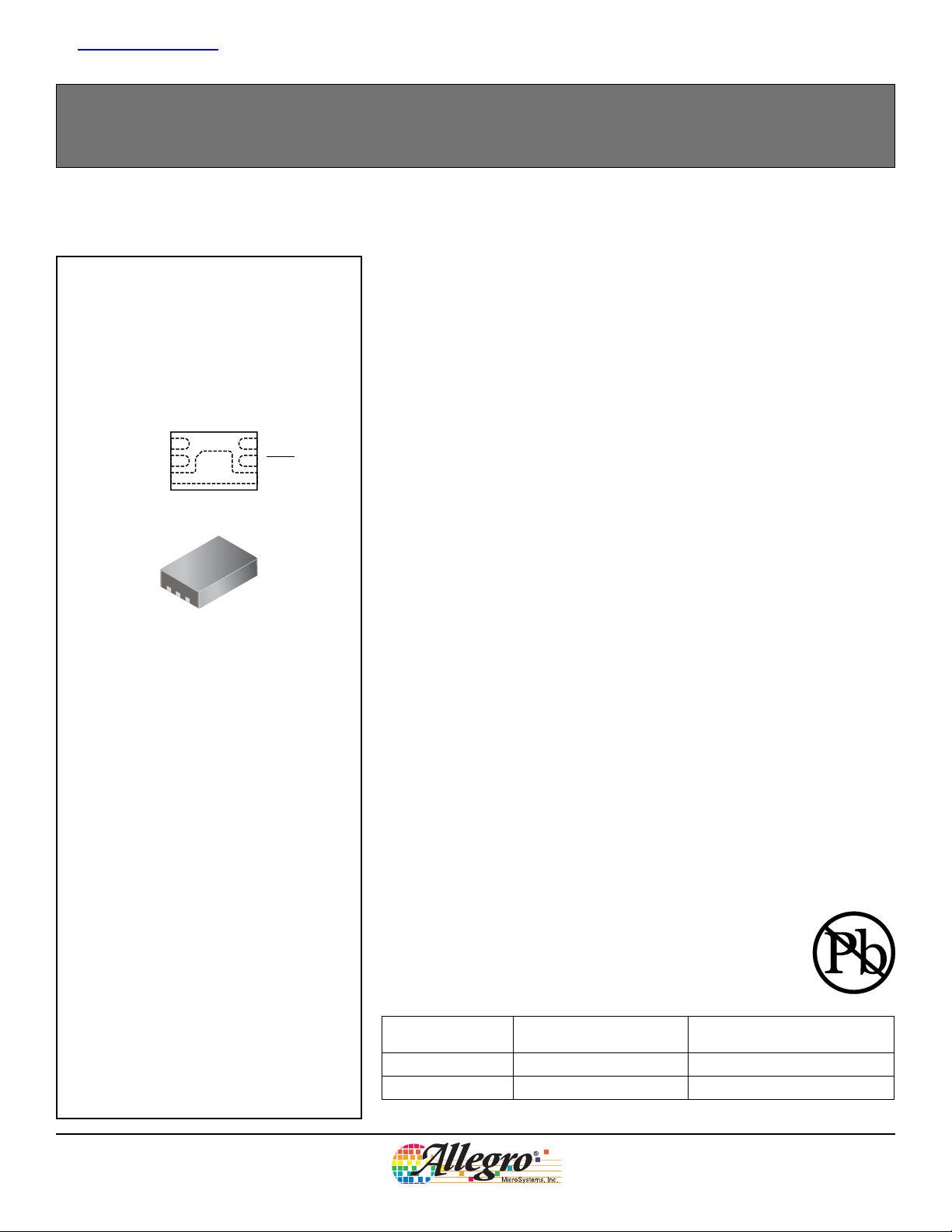
Package EH, 6-pin MLP/DFN
VREF
1
VCC
2
OUT
34
GND
6
5
SLEEP
GND
AB SO LUTE MAX I MUM RAT INGS*
than 3 mA of current. The A1391 and A1392 minimize current consumption to less than
25 μA through the addition of a user-selectable sleep mode. This makes these devices perfect for battery-operated applications such as: cellular phones, digital cameras, and portable
tools. End users can control the current consumption of the A1391 and A1392 by applying
a logic level signal to the ¯S¯ ¯L¯ ¯E¯ ¯E¯ ¯P¯ pin. The outputs of the devices are not valid (high-imped-
ance mode) during sleep mode. The high-impedance output feature allows the connection of
multiple A1391 and A1392 Hall effect devices to a single A-to-D converter input.
The quiescent output voltage of these devices is 50 % nominal of the ratiometric supply
reference voltage applied to the VREF pin of the device. The output voltage of the device is
not ratiometric with respect to the SUPPLY pin.
Despite the low power consumption of the circuitry in the A1391 and A1392, the features
required to produce a highly-accurate linear Hall effect IC have not been compromised.
Each BiCMOS monolithic circuit integrates a Hall element, improved temperature-compensating circuitry to reduce the intrinsic sensitivity drift of the Hall element, a small-signal
high-gain amplifier, and proprietary dynamic offset cancellation circuits. End of line, postpackaging, factory programming allows precise control of device sensitivity and offset.
This device is available in a small 2.0 × 3.0 mm, 0.75 mm nominal height micro leaded package (MLP). It is Pb (lead) free, with 100 % matte tin leadframe plating.
Supply Voltage, V
Reverse-Supply Voltage, V
.............................................8 V
CC
.......................–0.1 V
RCC
Ratiometric Supply Reference Voltage, V
Reverse-Ratiometric Supply
Reference Voltage, V
Logic Supply Voltage, V
(V
> 2.5 V)...............................................32 V
CC
Reverse-Logic Supply Voltage, V
Output Voltage, V
OUT
Reverse-Output Voltage, V
.........................–0.1 V
RREF
¯S¯ ¯L¯ ¯E¯ ¯E¯ ¯P¯
R¯S¯ ¯L¯ ¯E¯ ¯E¯ ¯P¯
............................ VCC + 0.1 V
......................–0.1 V
ROUT
Temperatures
Operating Ambient, T
Junction, T
Storage, T
*All ratings with reference to ground.
A1391-DS
J(MAX)
.................................–65ºC to 170ºC
S
, Range S .... –20ºC to 85ºC
A
.......................................165ºC
......7 V
REF
.........–0.1 V
Features and Benefits
• High-impedance output during sleep mode
• Compatible with 2.5 to 3.5 V power supplies
• 10 mW power consumption in the active mode
• Miniature MLP package
• Ratiometric output scales with the ratiometric supply reference voltage (VREF pin)
• Temperature-stable quiescent output voltage and sensitivity
• Wide ambient temperature range: –20°C to 85°C
• ESD protection greater than 3 kV
• Solid-state reliability
• Preset sensitivity and offset at final test
Use the following complete part numbers when ordering:
Part Number
A1391SEHLT-T
A1392SEHLT-T 2.50 7-in. reel, 3000 pieces/reel
*Contact Allegro for additional packing options.
Sensitivity
(mV / G, Typ.)
1.25
Packing*
7-in. reel, 3000 pieces/reel
Allegro MicroSystems, Inc.
115 Northeast Cutoff, Box 15036
Worcester, Massachusetts 01615-0036 (508) 853-5000
www.allegromicro.com

A1391 and A1392
Micro Power 3 V Linear Hall Effect Sensor with Tri-State Output and User-Selectable Sleep Mode
Functional Block Diagram
VCC
SLEEP
Hall Element
Regulator
To all subcircuits
Amp Out
Cancellation
Dynamic Offset
Gain
Filter
Programming Logic
Circuit Reference Current
GND
Offset
R
R
Ratio
Ratio
VREF
/ 2
/ 2
OUT
A1391-DS
Terminal List Table
Pin Name Function
1 VCC Supply
2 OUT Output
3 GND Ground
4 GND Ground
5¯S¯ ¯L¯ ¯E¯ ¯E¯ ¯P¯ Toggle sleep mode
6 VREF Supply for ratiometric reference
Allegro MicroSystems, Inc.
115 Northeast Cutoff, Box 15036
Worcester, Massachusetts 01615-0036 (508) 853-5000
www.allegromicro.com
2
A1391 and A1392
Micro Power 3 V Linear Hall Effect Sensor with Tri-State Output and User-Selectable Sleep Mode
Device Characteristics Tables
ELECTRICAL CHARACTERISTICS valid through full operating ambient temperature range, unless otherwise noted
Characteristic Symbol Test Conditions Min. Typ.
Supply Voltage V
Nominal Supply Voltage V
Supply Zener Clamp Voltage V
Ratiometric Reference Voltage
2
Ratiometric Reference Zener Clamp Voltage V
CC
CCN
CCZICC
V
REF
REFZIVREF =
= 7 mA, TA = 25°C 6 8.3 – V
3 mA, TA = 25°C 6 8.3 – V
2.5 – 3.5 V
– 3.0 – V
2.5 – V
¯S¯ ¯L¯ ¯E¯ ¯E¯ ¯P¯ Input Voltage –0.1 – V
¯S¯ ¯L¯ ¯E¯ ¯E¯ ¯P¯ Input Threshold
V
V
Ratiometric Reference Input Resistance R
Chopper Stabilization Chopping Frequency f
¯S¯ ¯L¯ ¯E¯ ¯E¯ ¯P¯ Input Current
Supply Current
3
I
SLEEPVSLEEP
I
Quiescent Output Power Supply Rejection4PSR
1
Typical data are for initial design estimations only, and assume optimum manufacturing and application conditions, such as TA = 25°C. Performance
may vary for individual units, within the specified maximum and minimum limits.
2
Voltage applied to the VREF pin. Note that the V
voltages of less than 2.5 V.
3
If the VREF pin is tied to the VCC pin, the supply current would be I
4
fAC is any ac component frequency that exists on the supply line.
voltage must be less than or equal to Vcc. Degradation in device accuracy will occur with applied
REF
For active mode – 0.45 × V
INH
For sleep mode – 0.20 × V
INL
V
> V
REF
SLEEP
TA = 25°C
V
< V
SLEEP
, V
INH
CC = VCCN,
INL, VCC = VCCN,
250 – – kΩ
TA = 25°C
CC
V
C
CC = VCCN
V
SLEEP
= 25°C
T
A
V
SLEEP
, TA = 25°C – 200 – kHz
= 3 V, V
< V
> V
= V
CC
CCN
INL, VCC = VCCN,
, V
INH
CC = VCCN,
TA = 25°C
VOQfAC
< 1 kHz – –60 – dB
+ V
REF
/ R
REF
CC
–5 –MΩ
–1 –μA
– 0.025 – mA
– 3.2 – mA
1
CC
CC
Max. Units
CC
+ 0.5 V
CC
–V
–V
V
A1391-DS
Allegro MicroSystems, Inc.
115 Northeast Cutoff, Box 15036
Worcester, Massachusetts 01615-0036 (508) 853-5000
www.allegromicro.com
3
A1391 and A1392
Micro Power 3 V Linear Hall Effect Sensor with Tri-State Output and User-Selectable Sleep Mode
OUTPUT CHARACTERISTICS valid through full operating ambient temperature range, unless otherwise noted
Characteristic Symbol Test Conditions Min. Typ.
Output Voltage Saturation
2
Limits
Maximum Voltage Applied
to Output
Sensitivity
3
Quiescent Output V
Output Resistance
4
V
OUTH
V
OUTL
V
OUTMAXVSLEEP
Sens
OUTQTA
R
Output Load Resistance R
Output Load Capacitance C
Output Bandwidth BW
5,6
Noise
1
Typical data are for initial design estimations only, and assume optimum manufacturing and application conditions, such as TA = 25°C. Performance
may vary for individual units, within the specified maximum and minimum limits.
2
This test requires positive and negative magnetic fields sufficient to swing the output driver between fully OFF and saturated (ON), respectively. The
value of vector X is NOT intended to indicate a range of linear operation.
3
For V
4
f
5
Noise specification includes digital and analog noise.
5
Values for BW
values other than V
REF
is the output signal frequency
OUT
externalLPF
do not include any noise resulting from noise on the externally-supplied VREF voltage.
REF
= V
V
CCN
B = X, V
B = –X, V
A1391 T
A1392 T
= V
CC
CC
< V
INL
= 25°C, V
A
= 25°C, V
A
= V
CCN
CCN
, V
, V
REF
REF
CC
CC
≤ V
= V
= V
≤ V
CC
REF
REF
CC
= V
= V
CCN
CCN
–V
– 0.1 – V
––V
1.18 1.25 1.31 mV/G
2.35 2.50 2.65 mV/G
= 25°C, B = 0 G – 0.500 × V
f
= 1 kHz, V
OUT
out
f
= 1 kHz, V
out
Output to ground 15 – – kΩ
L
Output to ground – – 10 nF
L
–3 dB point, V
V
= V
CC
CCN
C
bypass
1391
n
1392 C
, the sensitivity can be derived from the following equation: 0.416 × V
BW
C
bypass
bypass
> V
SLEEP
SLEEP
= 1 Vpp sinusoidal,
OUT
= 0.1 μF,
externalLPF
, active mode – 20 – Ω
INH
< V
, sleep mode – 4M – Ω
INL
– 10 – kHz
= 2 kHz
– 6 12 mV
= 0.1 μF, no load – – 20 mV
= 0.1 μF, no load – – 40 mV
1
– 0.1 – V
REF
REF
.
REF
Max. Units
+ 0.1 V
CC
(0.500 × V
REF
± 0.030
)
V
pp
pp
pp
A1391-DS
Allegro MicroSystems, Inc.
115 Northeast Cutoff, Box 15036
Worcester, Massachusetts 01615-0036 (508) 853-5000
www.allegromicro.com
4
A1391 and A1392
Micro Power 3 V Linear Hall Effect Sensor with Tri-State Output and User-Selectable Sleep Mode
OUTPUT TIMING CHARACTERISTICS1 T
Characteristic Symbol Test Conditions Min. Typ.
Power-On Time
Power-Off Time
1
See figure 1 for explicit timing delays.
2
Typical data are for initial design estimations only, and assume optimum manufacturing and application conditions, such as TA = 25°C. Performance
may vary for individual units, within the specified maximum and minimum limits.
3
Power-On Time is the elapsed time after the voltage on the SLEEP pin exceeds the active mode threshold voltage,V
reaches 90% of its value. When the device output is loaded with the maximum capacitance of 10 nF, the Power-On Time range is guaranteed for input
SLEEP pin frequencies less than 10 Hz.
4
Power-Off Time is the duration of time between when the signal on the SLEEP pin switches from HIGH to LOW and when ICC drops to under 100 μA.
During this time period, the output goes into the HIGH impedance state.
MAGNETIC CHARACTERISTICS T
3
4
t
PON
t
POFF
= 25°C
A
= 25°C
A
2
Max. Units
–40 60μs
–1 –μs
, until the time the device output
INH
Characteristic Symbol Test Conditions Min. Typ.* Max. Units
Ratiometry ΔV
Ratiometry ΔSens
Positive Linearity Lin+
Negative Linearity Lin –
Symmetry Sym
*Typical data are for initial design estimations only, and assume optimum manufacturing and application conditions, such as TA = 25°C. Performance
may vary for individual units, within the specified maximum and minimum limits.
OUTQ(ΔV)
(ΔV)
– 100 – %
– 100 – %
– 100 – %
– 100 – %
– 100 – %
A1391-DS
Allegro MicroSystems, Inc.
115 Northeast Cutoff, Box 15036
Worcester, Massachusetts 01615-0036 (508) 853-5000
www.allegromicro.com
5

A1391 and A1392
Micro Power 3 V Linear Hall Effect Sensor with Tri-State Output and User-Selectable Sleep Mode
Electrical Characteristic Data
Supply Current versus Ambient Temperature
A1391 and A1392, VCC = V
3.5
3.0
2.5
2.0
(mA)
1.5
CC
I
1.0
0.5
0
-20 -5 10 25 40 55 70 85
TA (°C)
REF
= 3 V
Active Mode
Sleep Mode
Ratiometric Reference Input Current
versus Ambient Temperature
19
17
15
13
11
(µA)
REF
I
A1391 and A1392, VCC = V
9
7
5
3
1
-20 -5 10 25 40 55 70 85
REF
= V
SLEEP
TA (°C)
SLEEP Input Current
versus Ambient Temperature
= 3 V A1391 and A1392, VCC = V
2.0
1.8
1.6
1.4
1.2
(µA)
1.0
0.8
SLEEP
I
0.6
0.4
0.2
0
-20 -5 10 25 40 55 70 85
T
(°C)
A
REF
= V
SLEEP
= 3 V
A1391-DS
Allegro MicroSystems, Inc.
115 Northeast Cutoff, Box 15036
Worcester, Massachusetts 01615-0036 (508) 853-5000
www.allegromicro.com
6

A1391 and A1392
)
Micro Power 3 V Linear Hall Effect Sensor with Tri-State Output and User-Selectable Sleep Mode
Magnetic Characteristic Data
Average Ratiometry, V
101.0
100.8
100.6
100.4
100.2
100.0
99.8
99.6
99.4
Average Ratiometry, Voq (%
99.2
99.0
-20-5102540557085
Average Ratiometry, Sens, versus Ambient Temperture
(A1391)
102.0
101.5
101.0
100.5
2.5 to 3 V
3.5 to 3 V
100.0
99.5
99.0
98.5
Average Ratiometr y, Sens (%)
98.0
97.5
-20-5102540557085
(°C)
T
A
, versus Ambient Temperture
OUTQ
(A139x)
2.5 to 3 V
3.5 to 3 V
T
(°C)
A
Average Ratiometry, Sens, versus Ambient Temperture
102.0
101.5
101.0
100.5
100.0
99.5
99.0
98.5
Average Ratiometr y, Sens (%)
98.0
97.5
-20-5102540557085
(A1392)
T
(°C)
A
2.5 to 3 V
3.5 to 3 V
Average Symmetry, Vcc=Vref=Vsleep=3V
102.0
101.5
101.0
100.5
100.0
99.5
99.0
Average Symetr y (%)
98.5
98.0
97.5
-20-5 102540557085
(A139x)
(°C)
T
A
102.0
101.5
101.0
100.5
100.0
99.5
99.0
98.5
Average Linearity (%)
98.0
97.5
97.0
-20-5 102540557085
A1391-DS
Average Linearity
(A139x)
Linearity - , Vcc=3.5V
Linearity +, Vcc=3.5V
Linearity +, Vcc=2.5V
Linearity -, Vcc = 2.5V
(°C)
T
A
Allegro MicroSystems, Inc.
115 Northeast Cutoff, Box 15036
Worcester, Massachusetts 01615-0036 (508) 853-5000
www.allegromicro.com
7

A1391 and A1392
Micro Power 3 V Linear Hall Effect Sensor with Tri-State Output and User-Selectable Sleep Mode
THERMAL CHARACTERISTICS may require derating at maximum conditions, see application information
Characteristic Symbol Test Conditions* Min. Units
1-layer PCB with copper limited to solder pads 221 ºC/W
Package Thermal Resistance
R
θJA
*For additional information, see Allegro Web site.
Power Dissipation versus Ambient Temperature
4500
4000
3500
3000
(mW)
D
2500
2000
1500
2-layer PCB with 0.6 in.
thermal vias
4-layer PCB based on JEDEC standard 50 ºC/W
4-layer PCB
(R
=50ºC/
θ
JA
W
2-layer PCB
(R
2
of copper area each side, connected by
)
70 ºC/W)
=
θJA
rPCB
e
1-lay
(R
θJA
C/W)
º
221
=
70 ºC/W
1000
Power Diss ipation, P
500
0
20 40 60 80 100 120 140 160 180
Temperature (°C)
A1391-DS
Allegro MicroSystems, Inc.
115 Northeast Cutoff, Box 15036
Worcester, Massachusetts 01615-0036 (508) 853-5000
www.allegromicro.com
8

A1391 and A1392
Micro Power 3 V Linear Hall Effect Sensor with Tri-State Output and User-Selectable Sleep Mode
Characteristics Definitions
Ratiometric. The A1391 and A1392 devices feature ratiometric
output. The quiescent voltage output and sensitivity are
proportional to the ratiometric supply reference voltage.
The percent ratiometric change in the quiescent voltage output is
defined as:
ΔV
OUTQ(ΔV)
ΔV
=
OUTQ(V
÷
)ΔVOUTQ(3V)
REF
V
÷ 3 V
REF
× 100 %
(1)
and the percent ratiometric change in sensitivity is defined as:
ΔSens
(ΔV)
ΔSens
=
ΔSens
÷
(V
)
÷ 3 V
(3V)
× 100%
(2)
REF
V
REF
Linearity and Symmetry. The on-chip output stage is
designed to provide a linear output with maximum supply voltage
of V
. Although application of very high magnetic fields will
CCN
not damage these devices, it will force the output into a non-linear region. Linearity in percent is measured and defined as
–
Lin+
Lin–
=
=
V
OUT(+B)
2(V
OUT(+B / 2)
V
OUT(–B)
2(V
OUT(–B / 2)
V
OUTQ
OUTQ
OUTQ
× 100 %
)
× 100 %
)
– V
–
V
OUTQ
– V
(3)
(4)
and output symmetry as
–
Sym
V
OUT(+B)
=
V
OUTQ
– V
V
OUTQ
OUT(–B)
× 100 %
(5)
A1391-DS
Allegro MicroSystems, Inc.
115 Northeast Cutoff, Box 15036
Worcester, Massachusetts 01615-0036 (508) 853-5000
www.allegromicro.com
9

A1391 and A1392
Micro Power 3 V Linear Hall Effect Sensor with Tri-State Output and User-Selectable Sleep Mode
Device Low-Power Functionality
A1391 and A1392 are low-power Hall effect sensor ICs that are
perfect for power sensitive customer applications. The current
consumption of these devices is typically 3.2 mA, while the
device is in the active mode, and less than 25 uA when the device
is in the sleep mode. Toggling the logic level signal connected to
the ¯S¯ ¯L¯ ¯E¯ ¯E¯ ¯P¯ pin drives the device into either the active mode or
the sleep mode. A logic low sleep signal drives the device into the
sleep mode, while a logic high sleep signal drives the device into
the active mode.
In the case in which the VREF pin is powered before the VCC
pin, the device will not operate within the specified limits until
the supply voltage is equal to the reference voltage. When the
device is switched from the sleep mode to the active mode, a time
defined by t
V
CC
V
SLEEP
must elapse before the output of the device is
PON
valid. The device output transitions into the high impedance state
approximately t
seconds after a logic low signal is applied to
POFF
the ¯S¯ ¯L¯ ¯E¯ ¯E¯ ¯P¯ pin (see figure 1).
If possible, it is recommended to power-up the device in the
sleep mode. However, if the application requires that the device
be powered on in the active mode, then a 10 kΩ resistor in series
with the ¯S¯ ¯L¯ ¯E¯ ¯E¯ ¯P¯ pin is recommended. This resistor will limit the
current that flows into the ¯S¯ ¯L¯ ¯E¯ ¯E¯ ¯P¯ pin if certain semiconductor
junctions become forward biased before the ramp up of the voltage on the VCC pin. Note that this current limiting resistor is not
required if the user connects the ¯S¯ ¯L¯ ¯E¯ ¯E¯ ¯P¯ pin directly to the VCC
pin. The same precautions are advised if the device supply is
powered-off while power is still applied to the ¯S¯ ¯L¯ ¯E¯ ¯E¯ ¯P¯ pin.
I
CC
+B
V
0
–B
OUT
HIGH
IMPEDANCE
t
PON
B field
Figure 1. A1391/A1392 Timing Diagram
A1391-DS
t
POFF
HIGH
IMPEDANCE
t
PON
HIGH
IMPEDANCE
t
POFF
Allegro MicroSystems, Inc.
115 Northeast Cutoff, Box 15036
Worcester, Massachusetts 01615-0036 (508) 853-5000
www.allegromicro.com
10

A1391 and A1392
Micro Power 3 V Linear Hall Effect Sensor with Tri-State Output and User-Selectable Sleep Mode
Device Supply Ratiometry Application Circuit
Figures 2 and 3 present applications where the VCC pin is connected together with the VREF pin of the A1391/A1392. Both
of these pins are connected to the battery, Vbat2. In this case, the
device output will be ratiometric with respect to the battery voltage.
The only difference between these two applications is that the
¯S¯ ¯L¯ ¯E¯ ¯E¯ ¯P¯ pin in figure 2 is connected to the Vbat2 potential, so the
device is always in the active mode. In figure 3, the ¯S¯ ¯L¯ ¯E¯ ¯E¯ ¯P¯ pin is
toggled by the microprocessor; therefore, the device is selectively
C
Vbat1
Supp ly pin
Micro-
processor
I/O
by pass
I/O
and periodically toggled between active mode and sleep mode.
In both figures, the device output is connected to the input of an
A-to-D converter. In this configuration, the converter reference
voltage is Vbat1.
It is strongly recommended that an external bypass capacitor be
connected, in close proximity to the A1391/-92 device, between
the VCC and GND pins of the device to reduce both external
noise and noise generated by the chopper-stabilization circuits
inside of the A1391/A1392.
Vbat2
VCC
VREF
A1391/A1392
OUT
SLEEP
GND GND
A1391-DS
Figure 2. Application circuit showing sleep mode disabled and output ratiometirc to the
A1391/A1392 supply.
Vbat1
Supp ly p in
Micro-
processor
I/O
by pass
I/O
Vbat 2
VCC
A1391/A1392
OUT
VREF
SLEEP
C
GND GND
Figure 3. Application circuit showing microprocessor-controlled sleep mode and output ratiometirc to the A1391/A1392 supply.
Allegro MicroSystems, Inc.
115 Northeast Cutoff, Box 15036
Worcester, Massachusetts 01615-0036 (508) 853-5000
www.allegromicro.com
11

A1391 and A1392
Micro Power 3 V Linear Hall Effect Sensor with Tri-State Output and User-Selectable Sleep Mode
Application Circuit with User-Configurable Ratiometry
In figures 4 and 5, the microprocessor supply voltage determines
the ratiometric performance of the A1391/A1392 output signal.
As in the circuits shown in figures 2 and 3, the device is powered
by the Vbat2 supply, but in this case, ratiometry is determined by
the microprocessor supply, Vbat1.
The ¯S¯ ¯L¯ ¯E¯ ¯E¯ ¯P¯ pin is triggered by the output logic signal from the
microprocessor in figure 5, while in figure 4, the ¯S¯ ¯L¯ ¯E¯ ¯E¯ ¯P¯ pin is
connected to the device power supply pin. Therefore, the device
as configured in figure 4 is constantly in active mode, while
the device as confiugred in figure 5 can be periodically toggled
C
filter
Vbat
1
C
bypass
Supply pin
Micro-
I/O
processor
I/O
between the active and sleep modes.
The capacitor C
is optional, and can be used to prevent pos-
filter
sible noise transients from the microprocessor supply reaching
the device reference pin, VREF.
It is strongly recommended that an external bypass capacitor
be connected, in close proximity to the A1391/A1392 device,
between the VCC and GND pins of the device to reduce both
external noise and noise generated by the chopper-stabilization
circuits inside of the A1391/A1392.
Vbat2
VCC
VREF
A1391/A1392
OUT
SLEEP
GND GND
A1391-DS
Figure 4. Application circuit showing ratiometry of V
. Sleep mode is disabled and the VREF
REF
pin is tied to the microprocessor supply.
bypass
Vbat2
VCC
A1391/A1392
OUT
GND GND
VREF
SLEEP
Allegro MicroSystems, Inc.
115 Northeast Cutoff, Box 15036
Worcester, Massachusetts 01615-0036 (508) 853-5000
www.allegromicro.com
C
Vbat1
filter
Supply pin
Micro-
processor
I/O
Figure 5. Application circuit showing device reference pin, VREF, tied to microprocessor supply. The device
sleep mode also is controlled by the microprocessor.
C
I/O
12

A1391 and A1392
Micro Power 3 V Linear Hall Effect Sensor with Tri-State Output and User-Selectable Sleep Mode
Summary of Single-Device Application Circuits
Device Pin Connections
Application Circuit
VREF pin (Ratiometric
Reference Supply)
¯S¯ ¯L¯ ¯E¯ ¯E¯ ¯P¯ pin
Device Output
C
Vbat1
Vbat1
filter
Vbat
Supp ly p in
processor
I/O
Supp ly p in
I/O
1
Micro-
Micro-
processor
Supply pin
Micro-
processor
I/O
C
I/O
C
by pass
I/O
by pass
I/O
C
Vbat2
bypass
Vbat 2
Vbat2
VCC
A1391/A1392
OUT
GND GND
VCC
A1391/A1392
OUT
GND GND
VCC
OUT
VREF
SLEEP
VREF
SLEEP
A1391/A1392
VREF
SLEEP
Connected to
A1391/A1392 device
supply, VCC
Connected to
A1391/A1392 device
supply, VCC
Connected to
microprocessor supply
Connected to
A1391/A1392 device
supply, VCC
Controlled by
microprocessor
Connected to
A1391/A1392 device
supply, VCC
Ratiometric to device
supply (VCC), and
always valid
Ratiometric to device
supply (VCC), and
controlled by the
microprocessor
Ratiometric to microprocessor supply, and
always valid
C
filter
A1391-DS
Vbat1
Supply pin
Micro-
processor
I/O
GND GND
Vbat2
C
bypass
VCC
I/O
OUT
A1391/A1392
SLEEP
VREF
Connected to
microprocessor supply
Controlled by
microprocessor
Ratiometric to microprocessor supply,
and controlled by the
microprocessor
GND GND
Allegro MicroSystems, Inc.
115 Northeast Cutoff, Box 15036
Worcester, Massachusetts 01615-0036 (508) 853-5000
www.allegromicro.com
13

A1391 and A1392
Micro Power 3 V Linear Hall Effect Sensor with Tri-State Output and User-Selectable Sleep Mode
Application Circuit with Multiple Hall Devices and a Single A-to-D Converter
Multiple A1391/A1392 devices can be connected to a single
microprocessor or A-to-D converter input. In this case, a
single device is periodically triggered and put into active
mode by the microprocessor. While one A1391/A1392 device
is in active mode, all of the other A1391/A1392 devices must
remain in sleep mode. While these devices are in sleep mode,
their outputs are in a high-impedance state. In this circuit
configuration, the microprocessor reads the output of
C
Vbat1
filter
A1
A2
Supp ly pin
Micro processor
A1
A2
A3
A4
one device at a time, according to microprocessor input to the
¯S¯ ¯L¯ ¯E¯ ¯E¯ ¯P¯ pins.
When multiple device outputs are connected to the same
microprocessor input, pulse timing from the microprocessor (for example, lines A1 through A4 in figure 6) must be
configured to prevent more than one device from being in the
awake mode at any given time of the application. A device
output structure can be damaged when its output voltage is
forced above the device supply voltage by more than 0.1 V.
C
Vbat2
bypass
VCC
VREF
A1391/A1392
OUT
SLEEP
GND GND
Vbat2
C
bypass
VCC
VREF
A1391/A1392
OUT
SLEEP
GND GND
I/O
C
bypass
Vbat2
VCC
A1391/A1392
OUT
VREF
SLEEP
A1391-DS
A3
A4
Vbat2
C
bypass
GND GND
VCC
VREF
A1391/A1392
OUT
SLEEP
GND GND
Figure 6. Application circuit showing multiple A1391/A1392 devices, controlled by a single microprocessor.
Allegro MicroSystems, Inc.
115 Northeast Cutoff, Box 15036
Worcester, Massachusetts 01615-0036 (508) 853-5000
www.allegromicro.com
14

A1391 and A1392
Micro Power 3 V Linear Hall Effect Sensor with Tri-State Output and User-Selectable Sleep Mode
Package EH, 6-pin MLP
2.15
Preliminary dimensions, for reference only
(reference JEDEC MO-229 WCED)
Dimensions in millimeters
U.S. Customary dimensions (in.) in brackets, for reference only
Dimensions exclusive of mold flash, gate burrs, and dambar protrusions
Exact case and lead configuration at supplier discretion within limits shown
A
Terminal #1 mark area
Exposed thermal pad
B
C
Hall Element (not to scale); U.S. customary dimensions controlling
D
Active Area Depth, 0.34 [.013]
Reference pad layout (reference IPC7351); adjust as
E
necessary to meet application process requirements;
when mounting on a multilayer PCB, thermal vias at the
exposed thermal pad land can improve thermal
dissipation (reference EIA/JEDEC Standard JESD51-5)
0.50 .020
0.30 .012
E
1.00 .039
3.70 .146
1.25 .049
.085
1.85
.073
6
.0591
1.5
C
NOM
5X
0.30
6X
0.18
0.10 [.004]
0.05 [.002] M C
6
0.65
0.45
.012
.007
0.225
REF
C0.08 [.003]
.026
.018
C
M C A B
0.50 .020
.009
A
21
1
2
A
1
.0394
C
NOM
B
3.15
.124
2.85
.112
0.20
REF
0.05
.002
0.00
.000
.0482
1.224
B
NOM
SEATING
PLANE
0.80
0.70
.008
D
.031
.028
C
0.25 .010
0.25 .010
1
0.95
.037
1.042
NOM
6
.0410
The products described herein are manufactured under one or more of the following U.S. patents: 5,045,920; 5,264,783; 5,442,283; 5,389,889;
5,581,179; 5,517,112; 5,619,137; 5,621,319; 5,650,719; 5,686,894; 5,694,038; 5,729,130; 5,917,320; and other patents pending.
Allegro MicroSystems, Inc. reserves the right to make, from time to time, such de par tures from the detail spec i fi ca tions as may be required to permit
improvements in the per for mance, reliability, or manufacturability of its products. Before placing an order, the user is cautioned to verify that the
information being relied upon is current.
Allegro products are not authorized for use as critical components in life-support devices or sys tems without express written approval.
The in for ma tion in clud ed herein is believed to be ac cu rate and reliable. How ev er, Allegro MicroSystems, Inc. assumes no re spon si bil i ty for its use;
nor for any in fringe ment of patents or other rights of third parties which may result from its use.
Copyright © 2005 Allegro MicroSystems, Inc.
Allegro MicroSystems, Inc.
A1391-DS
115 Northeast Cutoff, Box 15036
Worcester, Massachusetts 01615-0036 (508) 853-5000
www.allegromicro.com
15
 Loading...