

ALLEGRO A1373, A1374 User Manual
查询A1373供应商查询A1373供应商
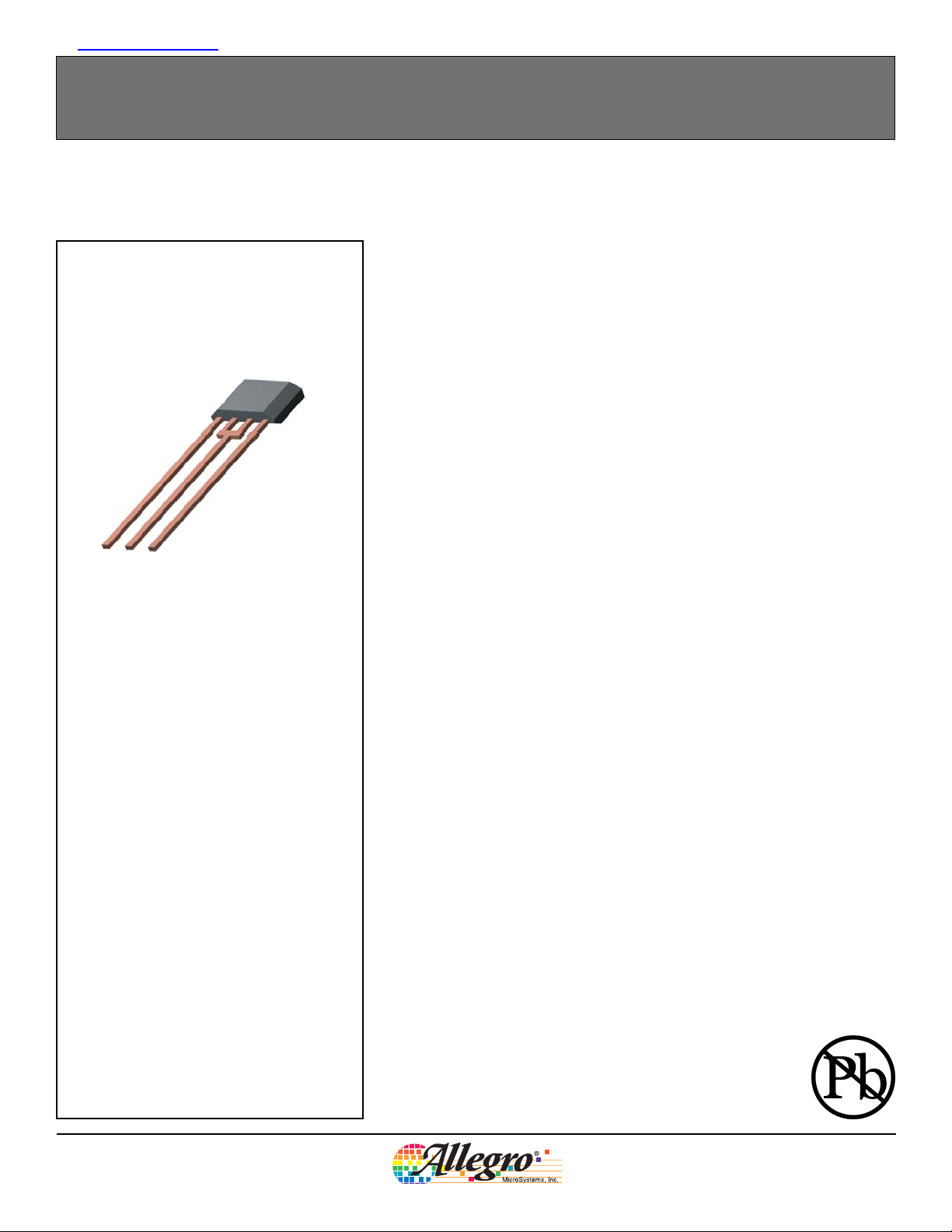
Package KB, 3-pin SIP
1
2
3
1. VCC
2. GND
3. VOUT (Programming)
A1373 and A1374
High Precision, Output Pin Programmable
Linear Hall Effect Sensors
The A1373 and A1374 high precision linear Hall effect sensors are sensitive, temperature stable, linear devices with externally programmable features. This device
family incorporates a chopper-stabilized amplifier, voltage regulator, programming logic, and an output amplifier on a single IC. The patented dynamic offset
cancellation used with a chopper-stabilization technique provides extremely low
offset and minimal temperature drift. A high frequency clock is used for chopping,
to ensure high frequency signal processing capability. The A1373 and A1374 are
ideal for use in automotive and industrial linear position-sensing applications that
require increased reliability and accuracy over conventional contacting-potentiometer solutions. Key applications include: throttle position sensors, pedal position
sensors, and suspension height sensors.
The design and manufacturing flexibility of the A1373 and A1374 complement
the Allegro linear Hall effect family of devices by offering programmable gain,
quiescent offset voltage for unipolar or bipolar operation, temperature coefficient, clamps, and polarity. The device can be set up in a magnetic circuit
and programmed with a train of serial pulses via the output pin. Once the right
combination of gain, quiescent output voltage, and temperature coefficient has
been selected, the codes can be locked for one-time programming. In this manner,
manufacturing tolerances can be reduced and the assembly process can be simplified.
These devices are available in the KB package, a 3-pin SIP (single inline package). The lead (Pb) free version has a 100% matte tin plated leadframe.
AB SO LUTE MAX I MUM RAT INGS
Supply Voltage, V
Reverse-Supply Voltage, V
Output Voltage
Reverse-Output Voltage, V
Output Current
Source, I
Sink, I
Operating Temperature
Ambient, T
Ambient, T
Maximum Junction, T
Storage Temperature, T
1
When blowing fuses during device programming, a
voltage of 28 V may be applied to VOUT.
A1373-DS, Rev. 3
OUTSOURCE
OUTSINK
..........................................16 V
CC
1
, V
OUT
.......................................... 10 mA
, Range E..................–40ºC to 85ºC
A
, Range L................–40ºC to 150ºC
A
........................ –16 V
RCC
....................................... 16 V
.....................–0.1 V
ROUT
................................... 3 mA
........................165ºC
J(max)
.................. –65ºC to 170ºC
S
Features and Benefits
Output pin programming
Field-programmable for optimal application integration
Selectable coarse and fine gain and quiescent output voltage
Selectable sensitivity temperature coefficient
Selectable output clamp voltage level, including no-clamp (rail-to-rail)
Selectable output polarity
Unipolar or bipolar operation
Ratiometric sensitivity, clamps, and quiescent output voltage
Chopper-stabilized Hall technique
Wide operating temperature range
On-chip regulator for over/under voltage protection
On-chip regulator provides EMI robustness
Wide lead-spacing with KB package
Allegro MicroSystems, Inc.
115 Northeast Cutoff, Box 15036
Worcester, Massachusetts 01615-0036 (508) 853-5000
www.allegromicro.com
A1373 and A1374
High Precision, Output Pin Programmable, Linear Hall Effect Sensors
Product Selection Guide
Part Number
A1373EKB –
A1373EKB–T Yes –40 to 85
A1373EKBTI –
A1373EKBTI–T Yes
A1373LKB –
A1373LKB–T Yes –40 to 150
A1373LKBTI –
A1373LKBTI–T Yes
A1374EKB –
A1374EKB–T Yes –40 to 85
A1374EKBTI –
A1374EKBTI–T Yes
A1374LKB –
A1374LKB–T Yes –40 to 150
A1374LKBTI –
A1374LKBTI–T Yes
*Contact Allegro for additional packing options
Pb-
free Packing*
Bulk, 500 pcs./bag
14.24-in. reel, 2000 pcs/reel
Bulk, 500 pcs./bag
14.24-in. reel, 2000 pcs/reel
Bulk, 500 pcs./bag
14.24-in. reel, 2000 pcs/reel
Bulk, 500 pcs./bag
14.24-in. reel, 2000 pcs/reel
Ambient, T
(ºC)
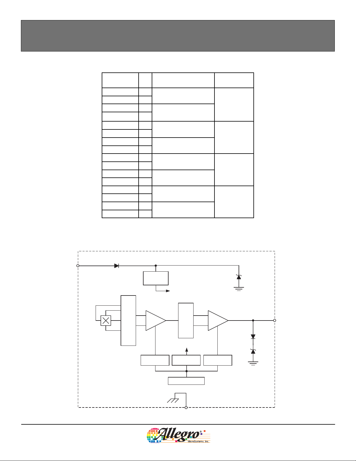
Functional Block Diagram
A
A1373-DS, Rev. 3
VCC
Pin 1
Cancellation
Dynamic Offset
Voltage
Regulator
To all subcircuits
Amp Out
Gain
Filter
Hall drive circuit
Temperature
Coefficient
Trim Control
GND
Pin 2
Offset
VOUT
Pin 3
Allegro MicroSystems, Inc.
115 Northeast Cutoff, Box 15036
Worcester, Massachusetts 01615-0036 (508) 853-5000
www.allegromicro.com
2
High Precision, Output Pin Programmable, Linear Hall Effect Sensors
CHARACTERISTIC PARAMETERS
Characteristic Symbol Test Conditions Min. Typ. Max Units
A1373 and A1374
ELECTRICAL CHARACTERISTICS
Supply Voltage V
Supply Current I
Reverse-Supply Current I
Power-On Time
1
Chopping Frequency f
over operating temperature range, VCC= 5.0 V, unless otherwise noted
CC
CC
RCC
t
PO
C
Internal Bandwidth BW
OUTPUT CHARACTERISTICS
2,3
Noise
Output Capacitance Load C
Output Resistive Load R
over operating temperature range, VCC= 5.0 V, unless otherwise noted
V
LOAD
LOAD
Phase Shift ΔΦ
V
OUT(Sat)HIGH
Output Voltage
V
OUT(Sat)LOW
Output Resistance R
OUT
MAGNETIC CHARACTERISTICS
Operation within specification,
< 165°C
T
j
4.5 5.0 5.5 V
– 8.2 10 mA
VCC = –16 V, TA = 25°C – – 16 mA
C
= 10 nF, 90% full scale V
LOAD
OUT
– – 300 μs
– 200 – kHz
A1373
A1374 – 20 – kHz
A1373
N
A1374 – 14 26 mV
Small signal -3 dB
peak-to-peak, C
LOAD
2.5 mV/G
> 1 nF,
– 2.5 – kHz
– 6 16 mV
VOUT pin to GND pin – – 10 nF
4700 – – Ω
A1373 Magnetic signal freq. = 100 Hz – 3 – (°)
A1374 Magnetic signal freq. = 1000 Hz – 3 – (°)
I
OUTSINK
B(kG) > (VCC–V
I
OUTSOURCE
B(kG) < V
= 1.2 mA,
OUT(Q)
= 1.2 mA,
/ Sens (mV/G)
OUT(Q)
) / Sens (mV/G)
4.65 4.7 – V
– 0.2 0.25 V
– 1.5 – Ω
Magnetic Slew Rate SLR V / ms / Sens – 20 –
PRE-PROGRAMMING TARGET (Prior to coarse and fine trim) over operating temperature range, V
= 5.0 V, unless
CC
otherwise noted
Pre-Programming Quiescent
Output Voltage
Pre-Programming Sensitivity Sens
Pre-Programming Sensitivity
Temperature Coefficient
INITIAL COARSE PROGRAMMING
Initial Coarse Quiescent Output
Voltage
Initial Coarse Sensitivity
V
OUT(Q)PRE
TC
PRE
PRE
B = 0 G, TA = 25°C 1.62 1.80 1.98 V
TA = 25°C 1.05 1.31 1.75 mV/G
TA relative to 25°C –0.016 0.05 0.104 %/°C
over operating temperature range, VCC= 5.0 V, unless otherwise noted
V
OUT(Q)INITLOWTA
V
OUT(Q)INITMID
V
OUT(Q)INITHIGHTA
Sens
INITLOW
Sens
INITMID
Sens
INITHIGHTA
= 25°C – 0.55 – V
Reference V
OUT(Q)PRE
––- –V
= 25°C – 3.25 – V
Reference Sens
PRE
– – – mV/G
TA = 25°C – 2.8 – mV/G
= 25°C – 5.5 – mV/G
Continued on the next page...
Allegro MicroSystems, Inc.
A1373-DS, Rev. 3
115 Northeast Cutoff, Box 15036
Worcester, Massachusetts 01615-0036 (508) 853-5000
www.allegromicro.com
G/μs
3
A1373 and A1374
High Precision, Output Pin Programmable, Linear Hall Effect Sensors
CHARACTERISTIC PARAMETERS (continued)
Characteristic Symbol Test Conditions Min. Typ. Max Units
QUIESCENT OUTPUT VOLTAGE PROGRAMMING over operating temperature range, V
V
OUT(Q)LOW
Quiescent Output Voltage Range
Average Quiescent Output Voltage
Step Size
4,5,6
Quiescent Output Voltage
Programming Resolution
V
OUT(Q)MID
V
OUT(Q)HIGH
Step
Err
PROGVOUT(Q)
Quiescent Output Voltage Drift
Over Operating Temperature
ΔV
Range
Quiescent Output Voltage
Programming Bits
V
10% Output Clamp Option
20% Output Clamp Option
7
7
Delay to Clamp t
SENSITIVITY PROGRAMMING
Sensitivity Range
Average Sensitivity Step Size
8
4,5,6
Sensitivity Programming
Resolution
Sensitivity
Programming Bits
OUTCLP10HIGH
V
OUTCLP10LOW
V
OUTCLP20HIGH
V
OUTCLP20LOW
over operating temperature range, VCC= 5.0 V, unless otherwise noted
Sens
Sens
Sens
Step
Step
Step
Err
VOUT(Q)
OUT(Q)
–
CLP
LOW
MID
HIGH
SENSLOW
SENSMID
SENSHIGH
PROGSENS
–
B = 0 G, TA = 25°C
TA = 25°C 3.0 3.275 3.5 mV
Fine programming value selection
accuracy
V
= V
OUT(Q)
V
OUT(Q)
V
OUT(Q)
OUT(Q)LOW
= V
OUT(Q)MID
= V
OUT(Q)HIGH
Coarse (Range selection) – 2 – Bit
Fine (Value selection) – 9 – Bit
A1373
A1374 4.300 – 4.650 V
A1373
A1374 0.3 – 0.6 V
A1373
A1374 3.900 – 4.200 V
A1373
A1374 0.8 – 1.1 V
High-side output clamp
Low-side output clamp
High-side output clamp
Low-side output clamp
A1373 – – 2 μs
A1374 – – 100 μs
TA = 25°C
TA = 25°C
Fine programming value selection
accuracy
Coarse (Range selection) – 2 – Bit
Fine (Value selection) – 8 – Bit
POLARITY PROGRAMMING
Polarity
Programming Bit
– Negative Sensitivity – 1 – Bit
= 5.0 V, unless otherwise noted
CC
0.7 – 1.9 V
2.0 – 3.2 V
3.5 – 4.5 V
–
±0.5 ×
Step
VOUT(Q)
–mV
– – ±40 mV
– – ±40 mV
– – ±55 mV
4.350 – 4.565 V
0.4 – 0.6 V
3.925 – 4.125 V
0.9 – 1.1 V
1.75 – 2.8 mV/G
3.5 – 5.7 mV/G
7.0 – 11.25 mV/G
6 9.5 14 μV/G
12 18.7 28 μV/G
22 37.0 56 μV/G
–
±0.5 ×
Step
SENS
– μV/G
Continued on the next page...
A1373-DS, Rev. 3
Allegro MicroSystems, Inc.
115 Northeast Cutoff, Box 15036
Worcester, Massachusetts 01615-0036 (508) 853-5000
www.allegromicro.com
4
A1373 and A1374
High Precision, Output Pin Programmable, Linear Hall Effect Sensors
CHARACTERISTIC PARAMETERS (continued)
Characteristic Symbol Test Conditions Min. Typ. Max Units
SENSITIVITY TEMPERATURE COEFFICIENT PROGRAMMING over operating temperature range, V
= 5.0 V, unless
CC
otherwise noted
Sensitivity T/C codes 0 to 11,
Sensitivity Temperature
Coefficient Range
TC
minimum (absolute) positive
temperature coefficient attainable
Sensitivity T/C codes 16 to 27,
minimum (absolute) negative
–
–
0.07
–
0.016 – %/°C
–
%/°C
temperature coefficient attainable
Average Sensitivity
Temperature Coefficient Step
6
4,5,
Size
Sensitivity Temperature
Coefficient Programming Bits
Step
TC
TA = 150°C
––
–
0.01
5
–
%/°C
– Bit
ONE-TIME PROGRAMMING
Device Programming Lock Bit
RATIOMETRY over operating temperature range, V
Quiescent Voltage Error
Sensitivity Error
Clamp Error Rat
LINEARITY
over operating temperature range, VCC= 5.0 V, unless otherwise noted
Positive Linearity Error Lin+ VCC at V
Negative Linearity Error
SYMMETRY
over operating temperature range, VCC= 5.0 V, unless otherwise noted
Symmetry Error
ADDITIONAL CHARACTERISTICS
Sensitivity Drift
9
FAULT CONDITIONS over operating temperature range, V
Shorted Output Wire
1
tPO does not include t
2
Peak to peak value exceeded: 0.3% (6σ).
3
For A1373, no digital noise is present at the output.
4
Step size is larger than required for the specified range, to take into account manufacturing spread.
5
Individual code step sizes can be greater than 2× larger than the step size at each significant bit rollover.
6
Average fine code step size in a given range = (Output value at highest fine code in the range – Output value at code 0 of the range) / Total quantity of
steps (codes) in the range.
7
Values indicated are valid if any additional magnetic field does not exceed B(kG)= ±2 (V) / Sens (mv/G), after V
8
Program the Sensitivity T/C register before programming Sensitivity Coarse and Sensitivity Fine, due to a worst case shift of ±3% in sensitivity at 25°C
at the maximum values for Sensitivity T/C: Positive T/C and Sensitivity T/C: Negative T/C. The Programming Guidelines section in this document lists a
complete recommended order for programming individual values.
9
Drift due to temperature cycling is due to package effects on the Hall transducer. The stress is reduced when the package is baked. However, it will
recover over time after removal from the bake.
, specified in the Quiescent Programming sectio n of this table.
CLP
– – 1 – Bit
= 5.0 V, unless otherwise noted
CC
Rat
Rat
VOUTCLP
VOUT(Q)
SENS
Lin–
Sym
VCC at V
VCC at V
VCC at V
VCC at V
VCC at V
OPERATING
OPERATING
OPERATING
OPERATING
OPERATING
OPERATING
– V
CC
–
–
–
–
–
–
±0.25
±1.0
±1.5
±0.5
±0.5
±0.35 –
–%
–%
–%
–%
–%
ΔSens – – ±2 %
= 5.0 V, unless otherwise noted
CC
I
OUTSHT
VOUT pin to VCC pin – – 18 mA
VOUT pin to GND pin – – 4 mA
is reached.
OUTCLP
%
A1373-DS, Rev. 3
Allegro MicroSystems, Inc.
115 Northeast Cutoff, Box 15036
Worcester, Massachusetts 01615-0036 (508) 853-5000
www.allegromicro.com
5
A1373 and A1374
High Precision, Output Pin Programmable, Linear Hall Effect Sensors
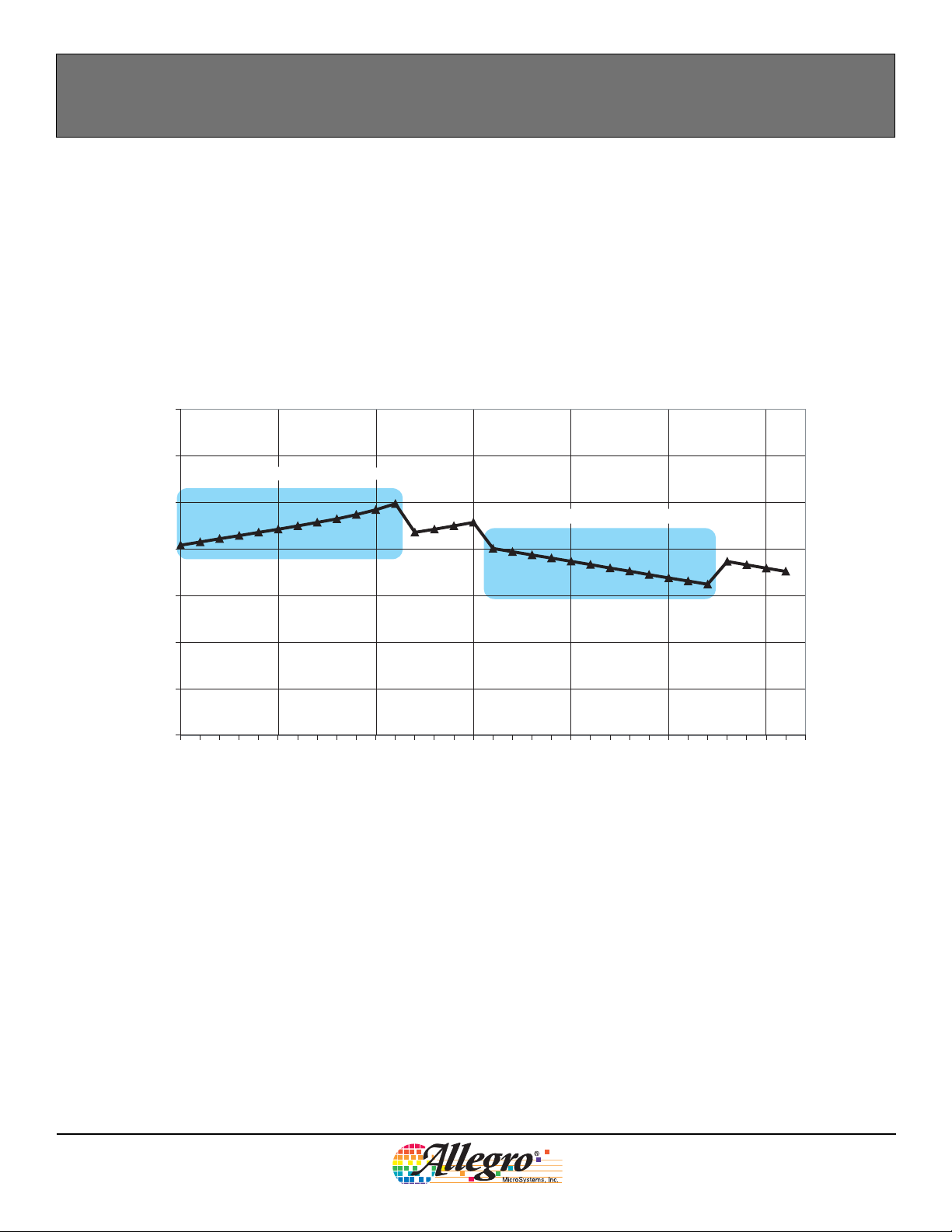
Typical Characteristics
Temperature Coefficient Code Profile
TA = 150°C, Magnetically Back-Biased
3.4
V
3.2
Positive Programming Codes
OUT(Q)
= V
OUT(Q)PRE
, Sens = 5 mV/G
3.0
Negative Programming Codes
(V)
2.8
OUT(Q)
2.6
V
2.4
2.2
2.0
0 5 10 15 20 25 30
Sensitivity TC Code
Code Application
0 Initial code
1 – 11 Positive TC codes, use to increase TC value
12 – 15 [Unused, same effect as 4 – 7, respectively]
16 – 27 Negative TC codes, use to decrease TC value
28 – 31 [Unused, same effect as 20 – 23, respectively]
A1373-DS, Rev. 3
Allegro MicroSystems, Inc.
115 Northeast Cutoff, Box 15036
Worcester, Massachusetts 01615-0036 (508) 853-5000
www.allegromicro.com
6
A1373 and A1374
High Precision, Output Pin Programmable, Linear Hall Effect Sensors
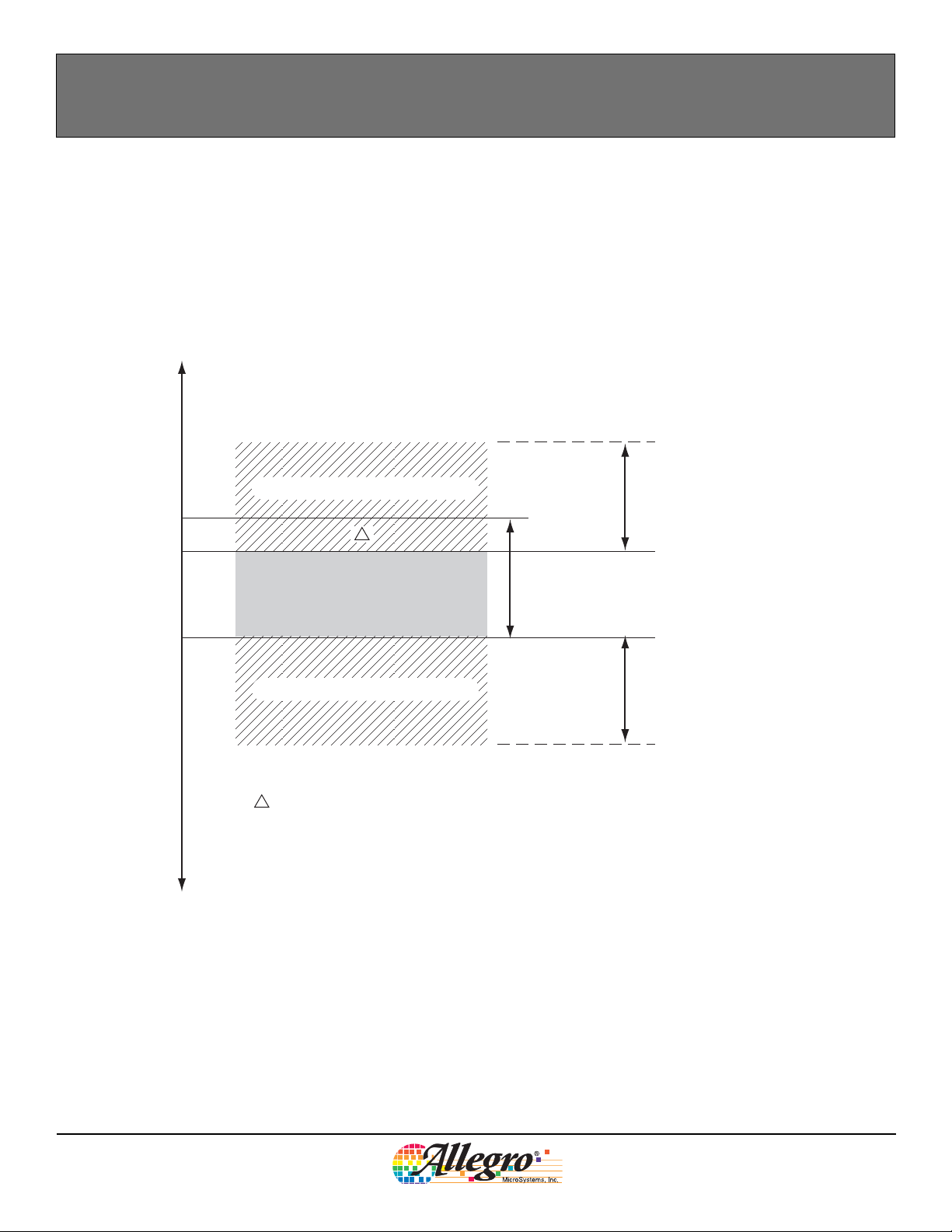
Sensitivity Temperature Coefficient Range, TC
0.25
0.20
0.15
0.10
0.05
0
TC (% / °C)
–0.05
–0.10
–0.15
–0.20
–0.25
Extended Range Not Guaranteed
TC
A
Guaranteed Programmable Range
Extended Range Not Guaranteed
A
Units with a TC in the range TC
< TC < TC
(min)
PRE(max)
TC Range Before Programming
PRE(max)
before programming may not be programmable
to the maximum attainable negative TC programming value
Typical maximum attainable
positive TC programming range
TC
(typ)
, for positive programming
TC
, for negative programming
(typ)
TC
PRE(min)
Typical maximum attainable
negative TC programming range
A1373-DS, Rev. 3
Allegro MicroSystems, Inc.
115 Northeast Cutoff, Box 15036
Worcester, Massachusetts 01615-0036 (508) 853-5000
www.allegromicro.com
7
 Loading...