

查询A1373供应商查询A1373供应商
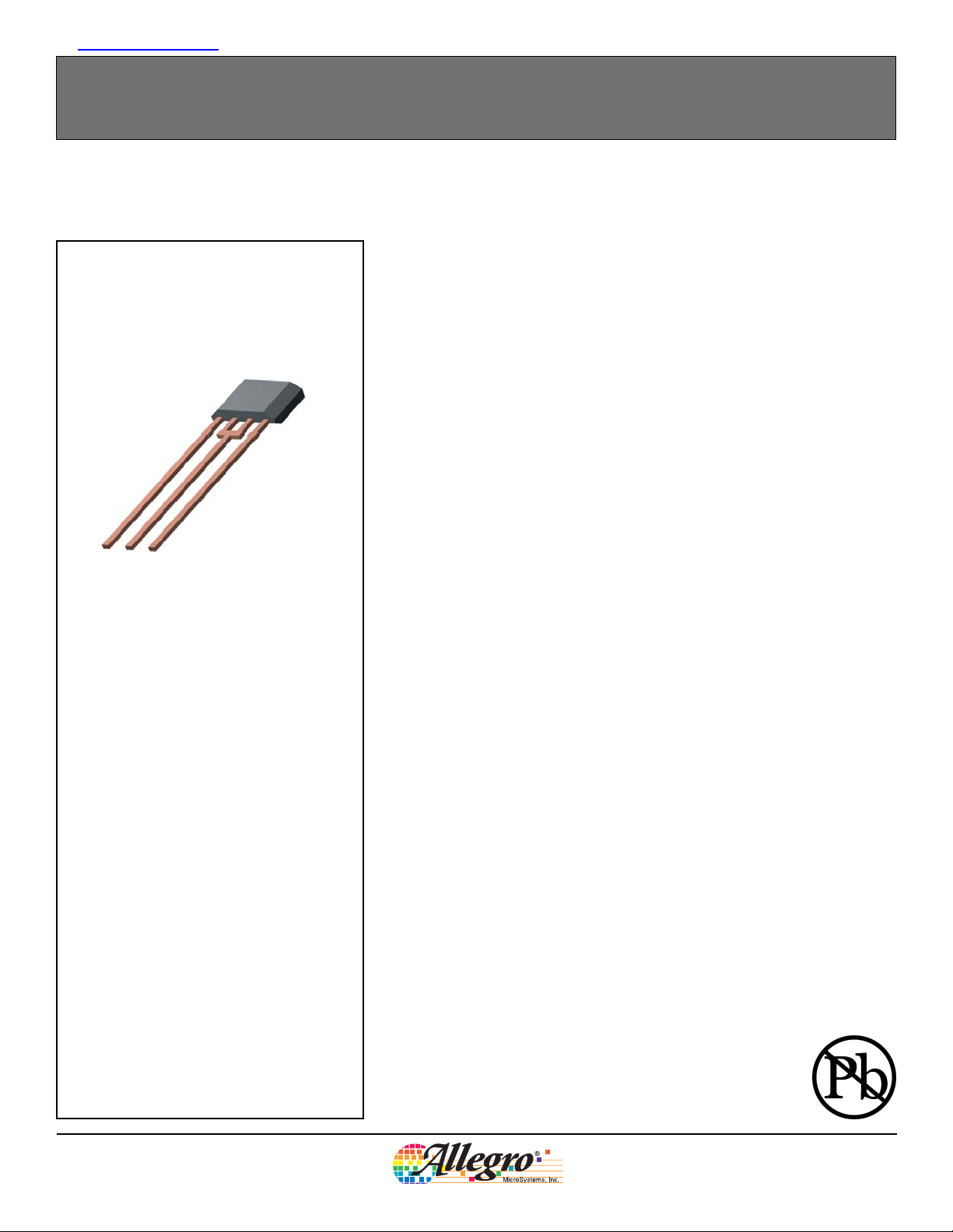
Package KB, 3-pin SIP
1
2
3
1. VCC
2. GND
3. VOUT (Programming)
A1373 and A1374
High Precision, Output Pin Programmable
Linear Hall Effect Sensors
The A1373 and A1374 high precision linear Hall effect sensors are sensitive, temperature stable, linear devices with externally programmable features. This device
family incorporates a chopper-stabilized amplifier, voltage regulator, programming logic, and an output amplifier on a single IC. The patented dynamic offset
cancellation used with a chopper-stabilization technique provides extremely low
offset and minimal temperature drift. A high frequency clock is used for chopping,
to ensure high frequency signal processing capability. The A1373 and A1374 are
ideal for use in automotive and industrial linear position-sensing applications that
require increased reliability and accuracy over conventional contacting-potentiometer solutions. Key applications include: throttle position sensors, pedal position
sensors, and suspension height sensors.
The design and manufacturing flexibility of the A1373 and A1374 complement
the Allegro linear Hall effect family of devices by offering programmable gain,
quiescent offset voltage for unipolar or bipolar operation, temperature coefficient, clamps, and polarity. The device can be set up in a magnetic circuit
and programmed with a train of serial pulses via the output pin. Once the right
combination of gain, quiescent output voltage, and temperature coefficient has
been selected, the codes can be locked for one-time programming. In this manner,
manufacturing tolerances can be reduced and the assembly process can be simplified.
These devices are available in the KB package, a 3-pin SIP (single inline package). The lead (Pb) free version has a 100% matte tin plated leadframe.
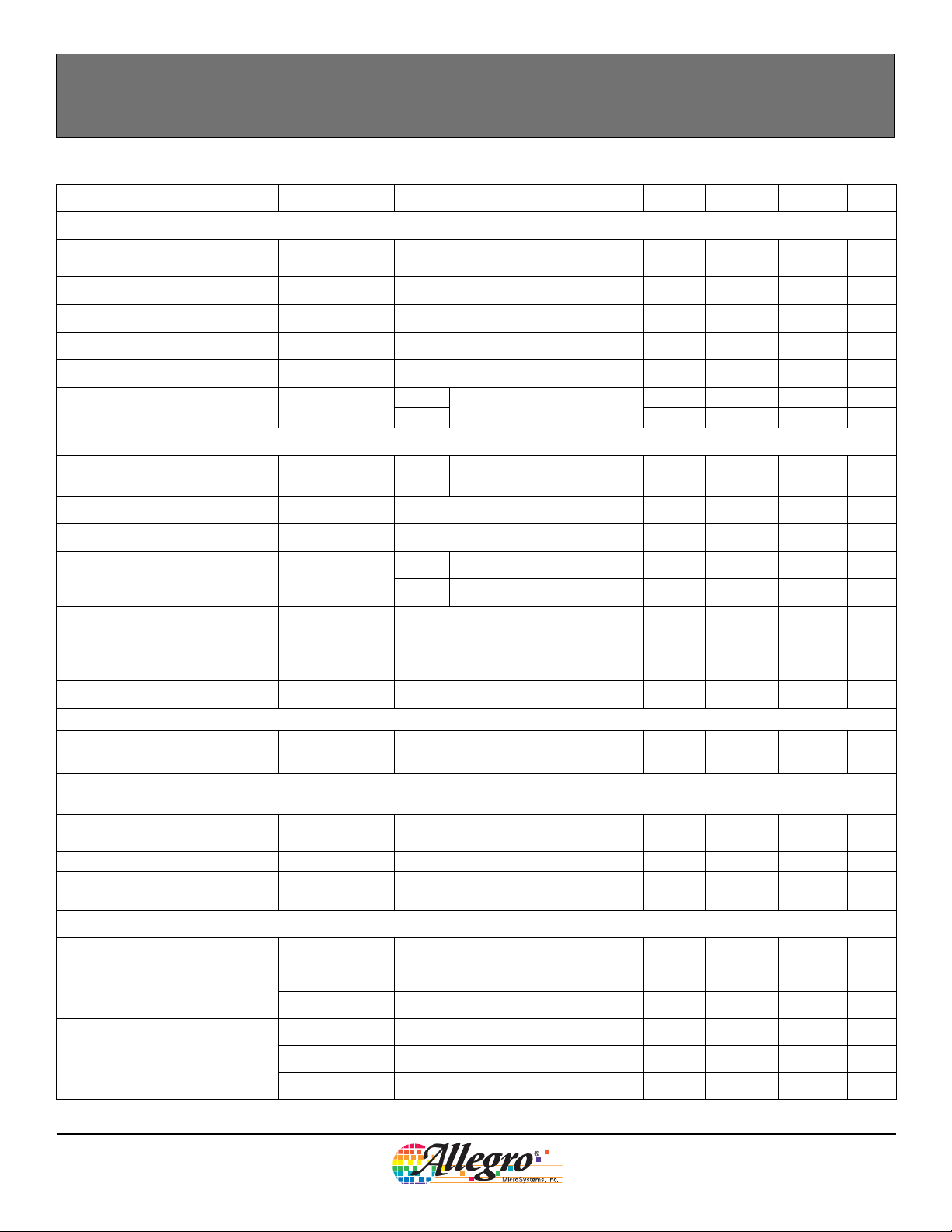
AB SO LUTE MAX I MUM RAT INGS
Supply Voltage, V
Reverse-Supply Voltage, V
Output Voltage
Reverse-Output Voltage, V
Output Current
Source, I
Sink, I
Operating Temperature
Ambient, T
Ambient, T
Maximum Junction, T
Storage Temperature, T
1
When blowing fuses during device programming, a
voltage of 28 V may be applied to VOUT.
A1373-DS, Rev. 3
OUTSOURCE
OUTSINK
..........................................16 V
CC
1
, V
OUT
.......................................... 10 mA
, Range E..................–40ºC to 85ºC
A
, Range L................–40ºC to 150ºC
A
........................ –16 V
RCC
....................................... 16 V
.....................–0.1 V
ROUT
................................... 3 mA
........................165ºC
J(max)
.................. –65ºC to 170ºC
S
Features and Benefits
Output pin programming
Field-programmable for optimal application integration
Selectable coarse and fine gain and quiescent output voltage
Selectable sensitivity temperature coefficient
Selectable output clamp voltage level, including no-clamp (rail-to-rail)
Selectable output polarity
Unipolar or bipolar operation
Ratiometric sensitivity, clamps, and quiescent output voltage
Chopper-stabilized Hall technique
Wide operating temperature range
On-chip regulator for over/under voltage protection
On-chip regulator provides EMI robustness
Wide lead-spacing with KB package
Allegro MicroSystems, Inc.
115 Northeast Cutoff, Box 15036
Worcester, Massachusetts 01615-0036 (508) 853-5000
www.allegromicro.com
A1373 and A1374
High Precision, Output Pin Programmable, Linear Hall Effect Sensors
Product Selection Guide
Part Number
A1373EKB –
A1373EKB–T Yes –40 to 85
A1373EKBTI –
A1373EKBTI–T Yes
A1373LKB –
A1373LKB–T Yes –40 to 150
A1373LKBTI –
A1373LKBTI–T Yes
A1374EKB –
A1374EKB–T Yes –40 to 85
A1374EKBTI –
A1374EKBTI–T Yes
A1374LKB –
A1374LKB–T Yes –40 to 150
A1374LKBTI –
A1374LKBTI–T Yes
*Contact Allegro for additional packing options
Pb-
free Packing*
Bulk, 500 pcs./bag
14.24-in. reel, 2000 pcs/reel
Bulk, 500 pcs./bag
14.24-in. reel, 2000 pcs/reel
Bulk, 500 pcs./bag
14.24-in. reel, 2000 pcs/reel
Bulk, 500 pcs./bag
14.24-in. reel, 2000 pcs/reel
Ambient, T
(ºC)
Functional Block Diagram
A
A1373-DS, Rev. 3
VCC
Pin 1
Cancellation
Dynamic Offset
Voltage
Regulator
To all subcircuits
Amp Out
Gain
Filter
Hall drive circuit
Temperature
Coefficient
Trim Control
GND
Pin 2
Offset
VOUT
Pin 3
Allegro MicroSystems, Inc.
115 Northeast Cutoff, Box 15036
Worcester, Massachusetts 01615-0036 (508) 853-5000
www.allegromicro.com
2
High Precision, Output Pin Programmable, Linear Hall Effect Sensors
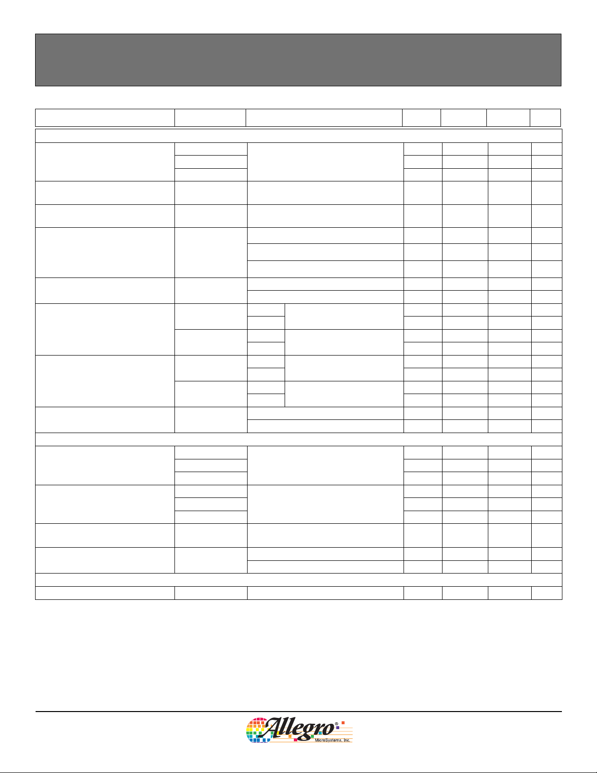
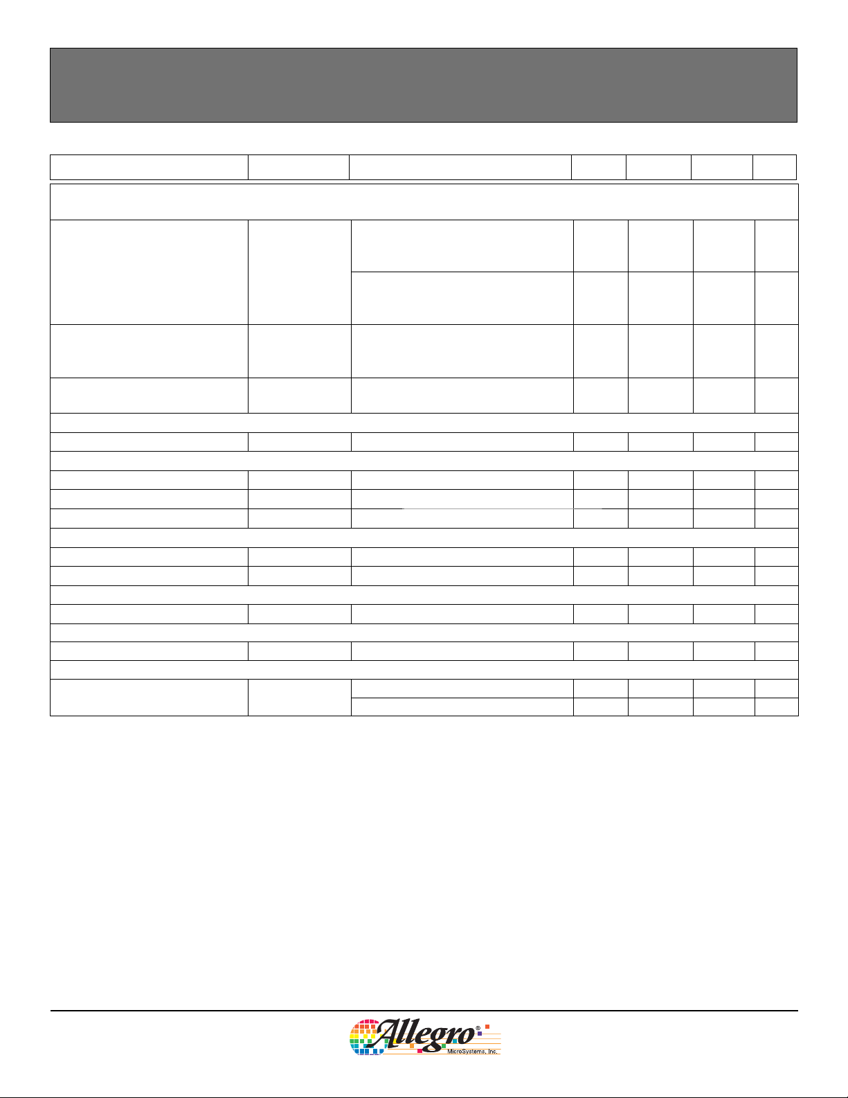
CHARACTERISTIC PARAMETERS
Characteristic Symbol Test Conditions Min. Typ. Max Units
A1373 and A1374
ELECTRICAL CHARACTERISTICS
Supply Voltage V
Supply Current I
Reverse-Supply Current I
Power-On Time
1
Chopping Frequency f
over operating temperature range, VCC= 5.0 V, unless otherwise noted
CC
CC
RCC
t
PO
C
Internal Bandwidth BW
OUTPUT CHARACTERISTICS
2,3
Noise
Output Capacitance Load C
Output Resistive Load R
over operating temperature range, VCC= 5.0 V, unless otherwise noted
V
LOAD
LOAD
Phase Shift ΔΦ
V
OUT(Sat)HIGH
Output Voltage
V
OUT(Sat)LOW
Output Resistance R
OUT
MAGNETIC CHARACTERISTICS
Operation within specification,
< 165°C
T
j
4.5 5.0 5.5 V
– 8.2 10 mA
VCC = –16 V, TA = 25°C – – 16 mA
C
= 10 nF, 90% full scale V
LOAD
OUT
– – 300 μs
– 200 – kHz
A1373
A1374 – 20 – kHz
A1373
N
A1374 – 14 26 mV
Small signal -3 dB
peak-to-peak, C
LOAD
2.5 mV/G
> 1 nF,
– 2.5 – kHz
– 6 16 mV
VOUT pin to GND pin – – 10 nF
4700 – – Ω
A1373 Magnetic signal freq. = 100 Hz – 3 – (°)
A1374 Magnetic signal freq. = 1000 Hz – 3 – (°)
I
OUTSINK
B(kG) > (VCC–V
I
OUTSOURCE
B(kG) < V
= 1.2 mA,
OUT(Q)
= 1.2 mA,
/ Sens (mV/G)
OUT(Q)
) / Sens (mV/G)
4.65 4.7 – V
– 0.2 0.25 V
– 1.5 – Ω
Magnetic Slew Rate SLR V / ms / Sens – 20 –
PRE-PROGRAMMING TARGET (Prior to coarse and fine trim) over operating temperature range, V
= 5.0 V, unless
CC
otherwise noted
Pre-Programming Quiescent
Output Voltage
Pre-Programming Sensitivity Sens
Pre-Programming Sensitivity
Temperature Coefficient
INITIAL COARSE PROGRAMMING
Initial Coarse Quiescent Output
Voltage
Initial Coarse Sensitivity
V
OUT(Q)PRE
TC
PRE
PRE
B = 0 G, TA = 25°C 1.62 1.80 1.98 V
TA = 25°C 1.05 1.31 1.75 mV/G
TA relative to 25°C –0.016 0.05 0.104 %/°C
over operating temperature range, VCC= 5.0 V, unless otherwise noted
V
OUT(Q)INITLOWTA
V
OUT(Q)INITMID
V
OUT(Q)INITHIGHTA
Sens
INITLOW
Sens
INITMID
Sens
INITHIGHTA
= 25°C – 0.55 – V
Reference V
OUT(Q)PRE
––- –V
= 25°C – 3.25 – V
Reference Sens
PRE
– – – mV/G
TA = 25°C – 2.8 – mV/G
= 25°C – 5.5 – mV/G
Continued on the next page...
Allegro MicroSystems, Inc.
A1373-DS, Rev. 3
115 Northeast Cutoff, Box 15036
Worcester, Massachusetts 01615-0036 (508) 853-5000
www.allegromicro.com
G/μs
3
A1373 and A1374
High Precision, Output Pin Programmable, Linear Hall Effect Sensors
CHARACTERISTIC PARAMETERS (continued)
Characteristic Symbol Test Conditions Min. Typ. Max Units
QUIESCENT OUTPUT VOLTAGE PROGRAMMING over operating temperature range, V
V
OUT(Q)LOW
Quiescent Output Voltage Range
Average Quiescent Output Voltage
Step Size
4,5,6
Quiescent Output Voltage
Programming Resolution
V
OUT(Q)MID
V
OUT(Q)HIGH
Step
Err
PROGVOUT(Q)
Quiescent Output Voltage Drift
Over Operating Temperature
ΔV
Range
Quiescent Output Voltage
Programming Bits
V
10% Output Clamp Option
20% Output Clamp Option
7
7
Delay to Clamp t
SENSITIVITY PROGRAMMING
Sensitivity Range
Average Sensitivity Step Size
8
4,5,6
Sensitivity Programming
Resolution
Sensitivity
Programming Bits
OUTCLP10HIGH
V
OUTCLP10LOW
V
OUTCLP20HIGH
V
OUTCLP20LOW
over operating temperature range, VCC= 5.0 V, unless otherwise noted
Sens
Sens
Sens
Step
Step
Step
Err
VOUT(Q)
OUT(Q)
–
CLP
LOW
MID
HIGH
SENSLOW
SENSMID
SENSHIGH
PROGSENS
–
B = 0 G, TA = 25°C
TA = 25°C 3.0 3.275 3.5 mV
Fine programming value selection
accuracy
V
= V
OUT(Q)
V
OUT(Q)
V
OUT(Q)
OUT(Q)LOW
= V
OUT(Q)MID
= V
OUT(Q)HIGH
Coarse (Range selection) – 2 – Bit
Fine (Value selection) – 9 – Bit
A1373
A1374 4.300 – 4.650 V
A1373
A1374 0.3 – 0.6 V
A1373
A1374 3.900 – 4.200 V
A1373
A1374 0.8 – 1.1 V
High-side output clamp
Low-side output clamp
High-side output clamp
Low-side output clamp
A1373 – – 2 μs
A1374 – – 100 μs
TA = 25°C
TA = 25°C
Fine programming value selection
accuracy
Coarse (Range selection) – 2 – Bit
Fine (Value selection) – 8 – Bit
POLARITY PROGRAMMING
Polarity
Programming Bit
– Negative Sensitivity – 1 – Bit
= 5.0 V, unless otherwise noted
CC
0.7 – 1.9 V
2.0 – 3.2 V
3.5 – 4.5 V
–
±0.5 ×
Step
VOUT(Q)
–mV
– – ±40 mV
– – ±40 mV
– – ±55 mV
4.350 – 4.565 V
0.4 – 0.6 V
3.925 – 4.125 V
0.9 – 1.1 V
1.75 – 2.8 mV/G
3.5 – 5.7 mV/G
7.0 – 11.25 mV/G
6 9.5 14 μV/G
12 18.7 28 μV/G
22 37.0 56 μV/G
–
±0.5 ×
Step
SENS
– μV/G
Continued on the next page...
A1373-DS, Rev. 3
Allegro MicroSystems, Inc.
115 Northeast Cutoff, Box 15036
Worcester, Massachusetts 01615-0036 (508) 853-5000
www.allegromicro.com
4
A1373 and A1374
High Precision, Output Pin Programmable, Linear Hall Effect Sensors
CHARACTERISTIC PARAMETERS (continued)
Characteristic Symbol Test Conditions Min. Typ. Max Units
SENSITIVITY TEMPERATURE COEFFICIENT PROGRAMMING over operating temperature range, V
= 5.0 V, unless
CC
otherwise noted
Sensitivity T/C codes 0 to 11,
Sensitivity Temperature
Coefficient Range
TC
minimum (absolute) positive
temperature coefficient attainable
Sensitivity T/C codes 16 to 27,
minimum (absolute) negative
–
–
0.07
–
0.016 – %/°C
–
%/°C
temperature coefficient attainable
Average Sensitivity
Temperature Coefficient Step
6
4,5,
Size
Sensitivity Temperature
Coefficient Programming Bits
Step
TC
TA = 150°C
––
–
0.01
5
–
%/°C
– Bit
ONE-TIME PROGRAMMING
Device Programming Lock Bit
RATIOMETRY over operating temperature range, V
Quiescent Voltage Error
Sensitivity Error
Clamp Error Rat
LINEARITY
over operating temperature range, VCC= 5.0 V, unless otherwise noted
Positive Linearity Error Lin+ VCC at V
Negative Linearity Error
SYMMETRY
over operating temperature range, VCC= 5.0 V, unless otherwise noted
Symmetry Error
ADDITIONAL CHARACTERISTICS
Sensitivity Drift
9
FAULT CONDITIONS over operating temperature range, V
Shorted Output Wire
1
tPO does not include t
2
Peak to peak value exceeded: 0.3% (6σ).
3
For A1373, no digital noise is present at the output.
4
Step size is larger than required for the specified range, to take into account manufacturing spread.
5
Individual code step sizes can be greater than 2× larger than the step size at each significant bit rollover.
6
Average fine code step size in a given range = (Output value at highest fine code in the range – Output value at code 0 of the range) / Total quantity of
steps (codes) in the range.
7
Values indicated are valid if any additional magnetic field does not exceed B(kG)= ±2 (V) / Sens (mv/G), after V
8
Program the Sensitivity T/C register before programming Sensitivity Coarse and Sensitivity Fine, due to a worst case shift of ±3% in sensitivity at 25°C
at the maximum values for Sensitivity T/C: Positive T/C and Sensitivity T/C: Negative T/C. The Programming Guidelines section in this document lists a
complete recommended order for programming individual values.
9
Drift due to temperature cycling is due to package effects on the Hall transducer. The stress is reduced when the package is baked. However, it will
recover over time after removal from the bake.
, specified in the Quiescent Programming sectio n of this table.
CLP
– – 1 – Bit
= 5.0 V, unless otherwise noted
CC
Rat
Rat
VOUTCLP
VOUT(Q)
SENS
Lin–
Sym
VCC at V
VCC at V
VCC at V
VCC at V
VCC at V
OPERATING
OPERATING
OPERATING
OPERATING
OPERATING
OPERATING
– V
CC
–
–
–
–
–
–
±0.25
±1.0
±1.5
±0.5
±0.5
±0.35 –
–%
–%
–%
–%
–%
ΔSens – – ±2 %
= 5.0 V, unless otherwise noted
CC
I
OUTSHT
VOUT pin to VCC pin – – 18 mA
VOUT pin to GND pin – – 4 mA
is reached.
OUTCLP
%
A1373-DS, Rev. 3
Allegro MicroSystems, Inc.
115 Northeast Cutoff, Box 15036
Worcester, Massachusetts 01615-0036 (508) 853-5000
www.allegromicro.com
5
A1373 and A1374
High Precision, Output Pin Programmable, Linear Hall Effect Sensors
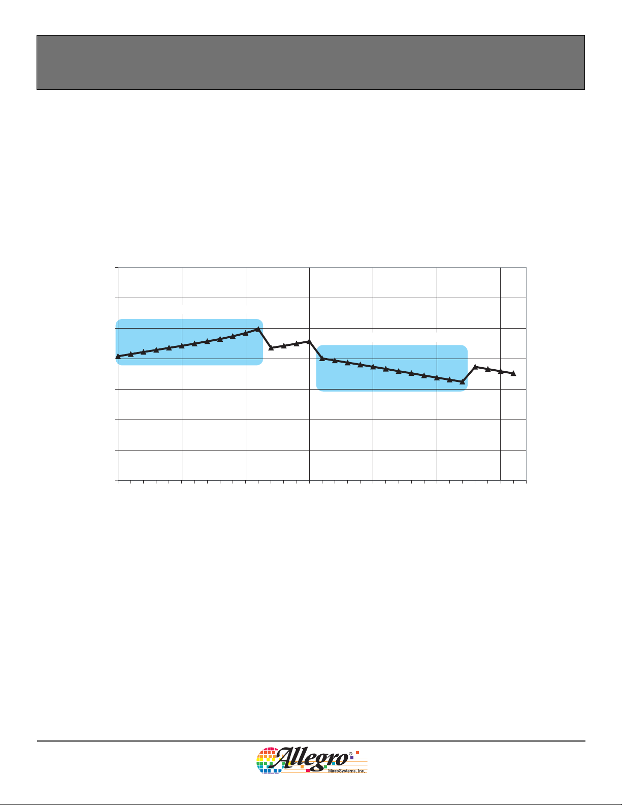
Typical Characteristics
Temperature Coefficient Code Profile
TA = 150°C, Magnetically Back-Biased
3.4
V
3.2
Positive Programming Codes
OUT(Q)
= V
OUT(Q)PRE
, Sens = 5 mV/G
3.0
Negative Programming Codes
(V)
2.8
OUT(Q)
2.6
V
2.4
2.2
2.0
0 5 10 15 20 25 30
Sensitivity TC Code
Code Application
0 Initial code
1 – 11 Positive TC codes, use to increase TC value
12 – 15 [Unused, same effect as 4 – 7, respectively]
16 – 27 Negative TC codes, use to decrease TC value
28 – 31 [Unused, same effect as 20 – 23, respectively]
A1373-DS, Rev. 3
Allegro MicroSystems, Inc.
115 Northeast Cutoff, Box 15036
Worcester, Massachusetts 01615-0036 (508) 853-5000
www.allegromicro.com
6
A1373 and A1374
High Precision, Output Pin Programmable, Linear Hall Effect Sensors
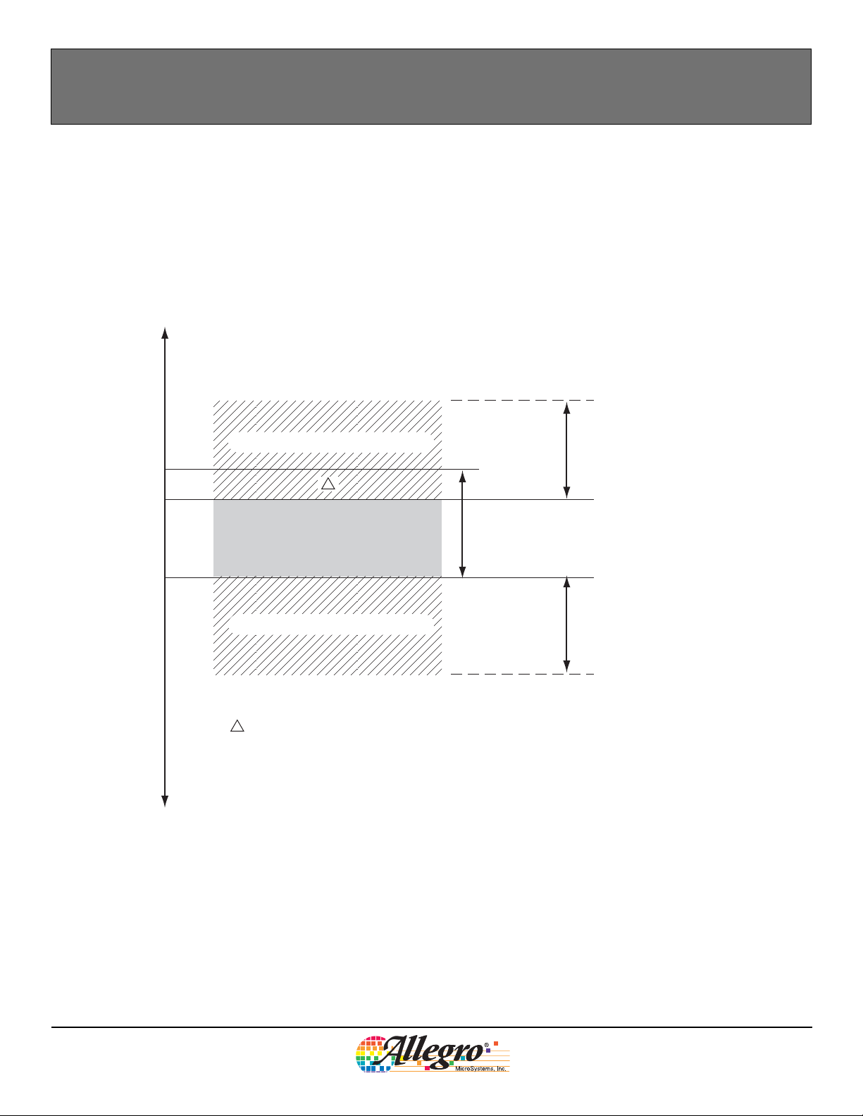
Sensitivity Temperature Coefficient Range, TC
0.25
0.20
0.15
0.10
0.05
0
TC (% / °C)
–0.05
–0.10
–0.15
–0.20
–0.25
Extended Range Not Guaranteed
TC
A
Guaranteed Programmable Range
Extended Range Not Guaranteed
A
Units with a TC in the range TC
< TC < TC
(min)
PRE(max)
TC Range Before Programming
PRE(max)
before programming may not be programmable
to the maximum attainable negative TC programming value
Typical maximum attainable
positive TC programming range
TC
(typ)
, for positive programming
TC
, for negative programming
(typ)
TC
PRE(min)
Typical maximum attainable
negative TC programming range
A1373-DS, Rev. 3
Allegro MicroSystems, Inc.
115 Northeast Cutoff, Box 15036
Worcester, Massachusetts 01615-0036 (508) 853-5000
www.allegromicro.com
7

A1373 and A1374
High Precision, Output Pin Programmable, Linear Hall Effect Sensors
Average Supply Current (Icc) vs Temperature
10.0
9.5
9.0
8.5
8.0
7.5
7.0
6.5
6.0
Average Supply Cur rent ( mA)
5.5
5.0
-50 -25 0 25 50 75 100 125 150
Average Ratiometry, Voq
101.0
100.8
100.6
100.4
100.2
100.0
99.8
99.6
99.4
Average Ratiom etry (Voq) (%)
99.2
99.0
-50-250255075100125150
4.5 to 5. 0 V
5.5 to 5. 0 V
Temperature (°C)
Vcc = 5V
Temperature ( °C)
101.0
100.8
100.6
100.4
100.2
100.0
99.8
99.6
99.4
99.2
Average Ratiom etry (Sens) (%)
99.0
-50-250255075100125150
Average Ratiometry, Sens
4.5 to 5. 0 V
5.5 to 5. 0 V
Temperature (°C)
101.0
100.8
100.6
100.4
100.2
100.0
99.8
99.6
99.4
Average Symmet ry (%)
99.2
99.0
-50 -25 0 25 50 75 100 125 150
A1373-DS, Rev. 3
Average Symmetry vs Temperature
Temperature (°C)
Average Linearity vs Temperature
101.0
100.8
100.6
100.4
100.2
100.0
99.8
99.6
Average Linear ity ( %)
99.4
99.2
99.0
-50 - 25 0 25 50 75 100 125 150
Temperature (°C)
Allegro MicroSystems, Inc.
115 Northeast Cutoff, Box 15036
Worcester, Massachusetts 01615-0036 (508) 853-5000
www.allegromicro.com
Lineari ty +
Lineari ty -
8

A1373 and A1374
High Precision, Output Pin Programmable, Linear Hall Effect Sensors
Average Delta Sensit ivity
(percent change relative to 25°C)
8
6
4
2
0
-2
Average Delta Sensiti vity ( %)
-4
-6
-50 -25 0 25 50 75 100 125 150
Sensitivity Low
Sensitivity Mid
Sensitivity High
Temperature ( °C)
Average Delta Sensit ivity
(percent per degree Celsius change relative to 25°C)
0.08
0.06
0.04
0.02
0
-0.02
-0.04
Average Delta Sensitvi ty (%/ °C)
-0.06
-0.08
-50 - 25 0 25 50 75 100 125 150
Sensitivity Low
Sensitivity Mid
Sensitivity High
Temperature ( °C)
Average Delta Sensit ivity over TC Codes
(percent change relative to 25°C)
Initial Coarse Ran ge
25
20
15
10
5
0
-5
Initial Delta Sensitivity (%)
-10
-15
-50 - 25 0 25 50 75 100 125 150
Sensitivity Low - TC Code 0
Sensitivity Low - TC Code 11
Sensitivity Low - TC Code 27
Temperature ( °C)
Average Delta Sensitivity
(percent per degree Celsius change relative to 25°C)
Initial Coarse Low
0.20
0.15
0.10
0.05
-0.05
-0.10
Average Delta Sensitvi ty (%/ °C)
-0.15
-0.20
Sensitivity Low - TC Code 0
Sensitivity Low - TC Code 11
Sensitivity Low - TC Code 27
0
-50 -25 0 25 50 75 100 125 150
Temperature ( °C)
15
10
5
0
TC Contribution to
Delta Sensitivity (%)
-5
-10
-50 -25 0 25 50 75 100 125 150
A1373-DS, Rev. 3
Positive TC Contribution to Delta Sensitivity
TC Code 1
TC Code 2
TC Code 4
TC Code 8
TC Code 11
Temperature (°C)
Negative TC Contribution to Delta Sensitivity
10
5
0
-5
-10
Sensitivity (%)
TC Contribution to Delta
-15
-20
-50 -25 0 25 50 75 100 125 150
TC Code 16
TC Code 17
TC Code 18
TC Code 20
TC Code 24
TC Code 27
Tem perature (°C)
Allegro MicroSystems, Inc.
115 Northeast Cutoff, Box 15036
Worcester, Massachusetts 01615-0036 (508) 853-5000
www.allegromicro.com
9

A1373 and A1374
High Precision, Output Pin Programmable, Linear Hall Effect Sensors
Average Quiescent Output Voltage
3.5
3.0
2.5
2.0
1.5
Average Vout(q) (V)
1.0
0.5
0
-50 -25 0 25 50 75 100 125 150
Average Quiescent Output Voltage
Max Code (511)
6
5
4
3
2
1
Average Vout(q) (max Code - 511) (V)
0
-50 -25 0 25 50 75 100 125 150
Vout(q)Low - Initial
Vout(q)Mid - Initial
Vout(q)High - Initial
Temperature (°C )
Vout(q)Low - Max Code
Vout(q)Mid - Max Code
Vout(q)High - Max Code
Temperature ( °C)
Average Delta Quiescent Output Voltage
Relative to 25°C, Initial Sensitivity
6
4
2
0
-2
-4
-6
Average Delta Vout(q) (mV)
-8
-10
-50 -25 0 25 50 75 100 125 150
Average Init ial Quiescent Output Voltage vs Supply Voltage
4.0
3.5
3.0
2.5
2.0
1.5
Average Vout(q) (V)
1.0
0.5
0
4 4.5 5 5.5 6
Temperature (°C)
= 25°C
T
A
Supply Voltage (V)
Vout(q)Low
Vout(q)Mid
Vout(q)High
Vout(q)Low - Initial
Vout(q)Mid - Initial
Vout(q)High - Initial
A1373-DS, Rev. 3
1.85
1.83
1.81
1.79
Average Vout(q) (V)
1.77
1.75
Average Quiescent Output Voltage over Sensitivity
Vout(q)Mid - SensLow
Vout(q)Mid - SensMid
Vout(q)Mid - SensHigh
-50 -25 0 25 50 75 100 125 150
Tempe rature (°C)
Allegro MicroSystems, Inc.
115 Northeast Cutoff, Box 15036
Worcester, Massachusetts 01615-0036 (508) 853-5000
www.allegromicro.com
10

A1373 and A1374
p
High Precision, Output Pin Programmable, Linear Hall Effect Sensors
5
Average Saturation Voltage
4
(V)
3
V
2
OUT(sat)
V
1
0
-50 -25 0 25 50 75 100 125 150
Temperature (°C)
OUT(sat)+
V
OUT(sat)–
5
Average Clamp Values
4
3
2
1
Average Clamp Vo ltage (V)
0
-50 -25 0 25 50 75 100 125 150
10% High Clamp
10% Low Clamp
20% High Clamp
20% Low Clam
Temperature (° C)
A1373-DS, Rev. 3
Allegro MicroSystems, Inc.
115 Northeast Cutoff, Box 15036
Worcester, Massachusetts 01615-0036 (508) 853-5000
www.allegromicro.com
11

A1373 and A1374
High Precision, Output Pin Programmable, Linear Hall Effect Sensors
Chopper Stabilization Technique
Chopper stabilization is a unique approach used to minimize
Hall offset on the chip. The patented Allegro technique, namely
Dynamic Quadrature Offset Cancellation, removes key sources
of the output drift induced by thermal and mechanical stresses.
This offset reduction technique is based on a signal modulationdemodulation process. The undesired offset signal is separated
from the magnetic field-induced signal in the frequency domain,
through modulation.
The subsequent demodulation acts as a modulation process for
the offset, causing the magnetic field-induced signal to recover
its original spectrum at baseband, while the dc offset becomes
a high-frequency signal. The magnetic-sourced signal then can
pass through a low-pass filter, while the modulated dc offset is
suppressed.
The chopper stabilization technique uses a 200 kHz high
frequency clock. For demodulation process, a sample and hold
technique is used, where the sampling is performed at twice the
chopper frequency (400 kHz). This high-frequency operation
allows a greater sampling rate, which results in higher accuracy
and faster signal-processing capability.
This approach desensitizes the chip to the effects of thermal and
mechanical stresses, and produces devices that have extremely
stable quiescent Hall output voltages and precise recoverability after temperature cycling. This technique is made possible
through the use of a BiCMOS process, which allows the use of
low-offset, low-noise amplifiers in combination with high-density logic integration and sample-and-hold circuits.
A1373-DS, Rev. 3
Hall Element
Regulator
Clock/Logic
Amp
Concept of Chopper Stabilization Technique
Low-Pass
Filter
Hold
Sample and
Allegro MicroSystems, Inc.
115 Northeast Cutoff, Box 15036
Worcester, Massachusetts 01615-0036 (508) 853-5000
www.allegromicro.com
12

A1373 and A1374
High Precision, Output Pin Programmable, Linear Hall Effect Sensors
Definitions of Terms
Linear: A type of Hall-Effect sensor that produces an analog output voltage proportional to the strength of a sensed magnetic field.
Ratiometric: A linear Hall-Effect sensor that, when not subjected to a significant magnetic field, has an output that is a ratio of its supply voltage.
A ratiometric performance of 100% indicates the output follows the supply with no percentage error.
Gauss: Standard unit of measuring magnetic flux density. 1 gauss is equal to 1 Maxwell per square centimeter or 10
earth’s magnetic field is approximately 0.5 gauss.)
-4
tesla. (For reference, the
Blowing: Applying a pulse of sufficient voltage and duration to permanently set a bit, by blowing a fuse internal to the device. Once a bit (fuse)
has been blown, it cannot be reset. The terms trimming and programming can be used interchangeably with blowing in this context.
Programming modes: Testing the results is the only valid method to guarantee successful programming, and multiple modes are provided to
support this. The programming modes are described in the section Mode Selection State.
Code: The number used to identify the register and the bitfield to be programmed, expressed as the decimal equivalent of the binary value. The LSB
of a register is denoted as bit 0.
Typical Application Drawing
V
REG
A1373-DS, Rev. 3
C
BYPASS
0.1 µF
VCC
A1373
A1374
GND
1
2
VOUT
3
R
LOAD
4.7 kΩ
Sensor Output
C
LOAD
1nF
Allegro MicroSystems, Inc.
115 Northeast Cutoff, Box 15036
Worcester, Massachusetts 01615-0036 (508) 853-5000
www.allegromicro.com
13

A1373 and A1374
V
CC
5V
=
× 100%
RAT
Sens
Sens
(VCC)
Sens
(5V)
=
× 100%
Lin+
2 (V
OUT(+B½)
–V
VOUTQ
)
–
V
OUT(+B)VOUTQ
=
× 100%
Lin–
2(V
OUT(–B½)–VOUTQ
)
–
V
OUT(–B)VOUTQ
–
=
× 100%
Sym
V
OUT(+B)
V
OUTQ–VOUT(–B)
V
OUTQ
=
RAT
VCLP
V
CC
5V
V
CLP(VCC)VCLP(5V)
× 100%
High Precision, Output Pin Programmable, Linear Hall Effect Sensors
Characteristic Definitions
Quiescent Output Voltage. In the quiescent state (no signifi-
cant magnetic field: B = 0), the output, V
, equals a ratio of
OUTQ
the supply voltage, VCC, throughout the entire operating ranges
of VCC and ambient temperature, TA. Due to internal component tolerances and thermal considerations, however, there is
a tolerance on the quiescent output voltage, ΔV
OUTQ
, which is
a function of both ΔVCC and ΔTA. For purposes of specification, the quiescent output voltage as a function of temperature,
ΔV
OUTQ(ΔTA)
, is defined as:
ΔV
OUTQ(ΔΤΑ)
V
OUTQ(ΤΑ)VOUTQ(25ºC)
=
Sens
–
(25ºC)
(1)
where Sens is in mV/G, and the result is the device equivalent
accuracy, in gauss (G), applicable over the entire operating temperature range.
Sensitivity. The presence of a south-polarity (+B) magnetic
field, perpendicular to the branded face of the device package,
increases the output voltage, V
field applied, from V
toward the VCC rail. Conversely, the
OUTQ
, in proportion to the magnetic
OUT
application of a north polarity (–B) magnetic field, in the same
orientation, proportionally decreases the output voltage from its
quiescent value. This proportionality is specified as the magnetic
sensitivity of the device and is defined as:
Sens
V
=
–
OUT(–B)VOUT(+B)
2B
(2)
The stability of the device magnetic sensitivity as a function of
ambient temperature, Δ Sens
ΔSens
(ΔΤΑ)
Sens
=
(%) is defined as:
( ΔTA)
Sens
–
(ΤΑ)
Sens
(25ºC)
(25ºC)
× 100%
(3)
proportional to the supply voltage, V
CC
.
The ratiometric change in the quiescent output voltage,
RAT
VOUT(Q)
RAT
(%), is defined as:
V
VOUT(Q)
=
OUTQ(VCC)
V
CC
V
OUTQ(5V)
5V
× 100%
(4)
the ratiometric change in sensitivity is defined as:
(5)
and the ratiometric change in clamp voltage is defined as:
(6)
Note that clamping effect is applicable only when clamping is
enabled by programming of the device.
Linearity and Symmetry. The on-chip output stage is
designed to provide linear output at a supply voltage of 5 V.
Although the application of very high magnetic fields does not
damage these devices, it does force their output into a nonlinear
(7)
(8)
region. Linearity in percent is measured and defined as:
(9)
Ratiometric. The A1373 and A1374 feature ratiometric
output. This means that the quiescent voltage output, V
magnetic sensitivity, Sens, and clamp voltage, V
A1373-DS, Rev. 3
OUTCLP
OUTQ
, are
,
and output symmetry as:
Allegro MicroSystems, Inc.
115 Northeast Cutoff, Box 15036
Worcester, Massachusetts 01615-0036 (508) 853-5000
www.allegromicro.com
14

A1373 and A1374
High Precision, Output Pin Programmable, Linear Hall Effect Sensors
Pulse Generation
Several parameters can be field-programmed. To do so, a coded
series of voltage pulses through the VOUT pin is used to set
bitfields in onboard registers. The effect on the device output can
be monitored, and the registers can be cleared and set repeatedly until the required output results are achieved. To make the
setting permanent, bitfield-level solid state fuses are blown, and
finally, a device-level fuse is blown, blocking any further coding.
Although any programmable variable power supply can be used
to generate the pulsed waveforms, Allegro highly recommends
using the Allegro Sensor Evaluation Kit, available on the Allegro
Web site On-line Store. The manual for that kit is available for
download free of charge, and provides additional information on
programming these devices.
There are four relative nominal voltage levels that must be taken
into account when programming. For purposes of explanation
in this document, the signal levels are referred to simply as high
programming voltage, V
, midrange, VPM, and low, VPL. The
PH
V
PH
Change State
1 < ΔtPH < 35 µs
fourth voltage level, V
, is a very low level, near zero volts, used
R
to reset the bitfields that have not yet been isolated by blown
fuses.
The high level, VPH, pulse is maintained either for short duration
(ΔtPH = 1 to <<35 μs), acting as a strobe to signal the transition
between states, or for long duration (ΔtPH ≥ 35 μs) and used for
fuse-blowing. The device generates an internal pulse beginning
at the leading (rising) edge of a VPH pulse. The duration of the
internal pulse is the duration of the external VPH pulse, ΔtPH,
plus 15 μs. The added time is a buffer to compensate for voltage drop when the high current is sourced, ensuring that there
is sufficient power to blow the fuse completely. Before sending
another pulse, an additional guard band of 5 μs is recommended
to allow the signal to decay, for a total of at least 20 μs after the
end of any VPH pulse. ΔtPH is measured from the time when the
external signal voltage rises above 23.6 V to the time when it
falls below 19.4 V. The nominal level for VPH is 28 V.
Blow Fuse
Δt
> 35 µs
PH
External Pulses
on VOUT Pin
Internal Pulses
Programming Pulse Waveforms
A1373-DS, Rev. 3
V
PM
V
PL
V
R
Logic 1
Logic 0
Guard
Band
(20 µs)
State Change or Blow pulse = ΔtPH +15 µs
Note: Spurious bit-setting pulses are generated on first V > V
Guard Band (6 µs)
Bit setting pulses = 5 µs
Blowing fuse
t
≥ 50 µs
min
after VR, and at last VPL.
PL
Allegro MicroSystems, Inc.
115 Northeast Cutoff, Box 15036
Worcester, Massachusetts 01615-0036 (508) 853-5000
www.allegromicro.com
15

A1373 and A1374
High Precision, Output Pin Programmable, Linear Hall Effect Sensors
The midrange voltage level, VPM, is a neutral level, used to
separate both VPH and VPL pulses from each other. The nominal
level for VPM is 15 V.
The low level, VPL, pulse is used to indicate bitfield addresses
that are to be set. The device generates an internal pulse beginning at the leading (falling) edge of a VPL pulse. The duration
of the internal pulse is 5 μs. Before allowing the voltage to
rise again, an additional guard band of 1 μs is recommended to
ensure that the pulse completes, for a total of at least 6 μs after
the start of any VPL pulse. The duration of the VPL pulse, ΔtPL ,
is measured from the time when the external signal voltage falls
into the range 0 to 7.5 V to the time when it rises above 10 V. If
the voltage rises above 10 V before the 5 μs period expires, then
the VPL pulse will immediately end, with undefined results. The
nominal level for VPH is 5 V.
VPL must always be maintained high enough above VR (nominally 0 V) to maintain the settings provisionally latched into
registers. Note that, when the external voltage rises from VR
through the VPL range, a spurious internal pulse is generated,
making Code 0 not available in Mode Selection state. A spurious
internal pulse also is generated when the external voltage falls
through the VPL range at the end of a code sequence. For that
reason, it is mandatory to ensure that the voltage is dropped fully
to VR, before every Blow Fuse mode operation, to ensure that
the spurious pulse does not affect the next code sequence.
A1373-DS, Rev. 3
Allegro MicroSystems, Inc.
115 Northeast Cutoff, Box 15036
Worcester, Massachusetts 01615-0036 (508) 853-5000
www.allegromicro.com
16
A1373 and A1374
High Precision, Output Pin Programmable, Linear Hall Effect Sensors
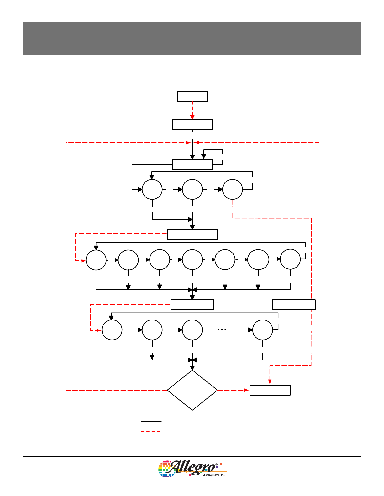
Programming State Machine
POWER UP
INITIAL STATE
V
PH
V
PH
MODE SELECT
V
PL
BLOWTRY LOCK
V
PL
V
PL
12 3
V
V
PH
PH
V
V
PL
PH
QVO
Coarse
01
V
PH
QVO
Fine
V
V
PH
V
PL
[Optional:
Measure]
V
PL
V
PH
REGISTER SELECT
SENS.
PL
Coarse
2
V
PH
[Optional:
Measure]
1 20 2^N -1
V
PH
No Yes
SENS.
V
PL
Fine
34 56
V
PH
BITFIELD SELECT BITFIELD SELECT
V
PL
SENS.
V
TC
V
PH
[Write Mode]
PL
[Optional:
Measure]
V
PL
V
V
PL
PH
BLOWING
MODE?
V
CLAMP
PL
V
PH
V
PL
V
PH
FUSE BLOWING
POLAR
V
PH
V
PL
V
PL
V
PH
A1373-DS, Rev. 3
User generated transition
Internally generated transition
Allegro MicroSystems, Inc.
115 Northeast Cutoff, Box 15036
Worcester, Massachusetts 01615-0036 (508) 853-5000
www.allegromicro.com
17

A1373 and A1374
High Precision, Output Pin Programmable, Linear Hall Effect Sensors
Programming Protocol and State Machine Description
INITIAL STATE
After system power-up, the programming logic is reset to a
known state. This is referred to as the Initial state. All the registers that have intact fuses are set to logic 0.
While in the Initial state, any VPL pulses on the VOUT pin are
ignored.
To enter the Mode Selection state, send one V
pulse on the
PH
VOUT pin.
MODE SELECTION STATE
This state allows the selection of the programming mode:
• Try Value Mode. In this mode, the user provisionally downloads
settings to the device registers, without blowing the bits. The user
can increment through the codes of each parameter, and evaluate the
results of various code settings.
• Blow Fuse Mode. In this mode, after downloading the settings, the
user can blow the fuses in specific registers.
• Lock Device Mode. This mode is similar to Blow Fuse mode, except
that the fuse that is blown permanently prevents any further programming of any bits in the device.
To select a mode, increment through the register bitfields by
sending VPL pulses on the VOUT pin, as follows:
0 pulses – No effect
1 pulse – Try Value mode
2 pulses – Blow Fuse mode
3 pulses – Lock Device mode
This register wraps by default. This means that sending additional VPL pulses traverses the register again.
Any VPH pulse sent before a VPL pulse has no effect.
To enter the Register Selection state, after sending a valid quantity of VPL pulses, send one VPH pulse on the VOUT pin.
REGISTER SELECTION STATE
This state allows the selection of the register containing the
bitfields to be programmed. Selecting the register corresponds to
selecting the parameter to be set. For bit codes, see the section
Programming Logic.
• QVO [V
ing dc point (2 bits)
• QVO Fine. Register for setting the value within the range set in the
QVO Coarse register (9 bits)
• Sens. [Sensivity] Coarse. Register for setting the overall gain of the
] Coarse. Register for setting the range of the operat-
OUT(Q)
device (2 bits)
• Sens. Fine. Register for setting the value within the range set in the
Sens. Coarse register (8 bits)
• [Sensitivity] TC Register. Register for setting the temperature coefficient for the device (5 bits).
• Clamp [V
the output (2 bits)
• Polarity Bit. Register setting the polarity of the output (1 bit)
] Bit. Register for setting the clamping voltage of
OUTCLP
To select a register, increment through the register bitfields by
sending V
pulses on the VOUT pin. Note that the program-
PL
ming of registers should follow the order shown in item 7 in the
section Programming Guidelines, not the bitfield selection order
shown here. The bitfield selection order is:
0 pulses – QVO Coarse register
1 pulse – QVO Fine register
2 pulses – Sens. Coarse register
3 pulses – Sense Fine register
4 pulses – TC Register register
5 pulses – Clamp Bit register
6 pulses – Polarity Bit register
This register wraps by default.
To enter the Register Selection state, send one VPH pulse on the
VOUT pin.
BITFIELD SELECTION STATE (Write Mode)
This state allows the selection of the individual bitfields to be
programmed, in the register selected in the Register Selection
state.
In Try Value mode, the total value of the bitfields selected increments by 1 with each VPL pulse on the VOUT pin. The parameter being programmed changes with each additional pulse, so
measurements can be taken after each pulse to determine if the
desired result has been acquired.
In Blow Fuses mode, each bitfield to be blown must be selected
individually.
For bit codes and wrapping for these registers, see the section
Programming Logic.
To leave this state, send one VPH pulse on the VOUT pin. If the
current mode is Try Value, the bitfields remain set and the device
reverts to the Mode Selection state. If the current mode is Blow
Fuse, the selected bitfield fuse is blown, and the device reverts to
the Mode Selection state.
A1373-DS, Rev. 3
Allegro MicroSystems, Inc.
115 Northeast Cutoff, Box 15036
Worcester, Massachusetts 01615-0036 (508) 853-5000
www.allegromicro.com
18

A1373 and A1374
High Precision, Output Pin Programmable, Linear Hall Effect Sensors
Programming Logic
Binary Bitfield Address Decimal Equivalent Code Description
QVO Coarse register
00 0 V
01 1 V
10 2 V
11 3 Register wraps to 00
QVO Fine register
000000000 0 Initial value in selected QVO Coarse range
111111111 511 Maximum value in selected QVO Coarse range
Sens. Coarse register
00 0 Sens low range
01 1 Sens mid range
10 2 Sens high range
11 3 Register wraps to 00
Sens. Fine register
00000000 0 Initial value in selected Sens. Coarse range
11111111 2 55 Maximum value in selected Sens. Coarse range
TC Register register (See also chart Sensitivity Temperature Coefficient Code Profile in Typical Characteristics section)
00000 0 initial TC
00001 through 01011 1 through 11 Positive TC programming range
01100 through 01111 1 2 through 15 Unused: equal to codes 4 to 7, respectively
10000 through 11011 16 through 27 Negative TC prgramming range; Value for 16 equals 1 step
11100 through 11111 28 through 31 Unused: equal to codes 20 to 23, respectively
Clamp Bit register
00 0 Rail-to-rail output swing
01 1 0.5 V and V
10 2 1 V and V
00 3 Register wraps to 00
Polarity Bit register
0 0 Positive (V
1 1 Negative (V
mid range
OUT(Q)
low range
OUT(Q)
high range
OUT(Q)
less than the value for the Initial TC Value (00000)
– 0.5V rails
CC
– 1 V rails
CC
increases when a positive (south) magnetic
field is applied to the device )
field is applied to the device )
OUT
increases when a negative (north) magnetic
OUT
A1373-DS, Rev. 3
Allegro MicroSystems, Inc.
115 Northeast Cutoff, Box 15036
Worcester, Massachusetts 01615-0036 (508) 853-5000
www.allegromicro.com
19

A1373 and A1374
High Precision, Output Pin Programmable, Linear Hall Effect Sensors
Programming Guidelines
• A bypass capacitor rated at 0.1μF must be mounted between
the VOUT pin and the GND pin during programming. The
power supply used for programming should be capable of delivering 28 V and 300 mA.
• Before beginning any Blow Fuse mode or Lock Device mode
code sequence, the device MUST be reset by cycling VCC
power-off and power-on again. Cycling power resets the device
by setting all bitfields that have intact fuses to 0. Bitfields with
blown fuses are unaffected.
In Try Value mode, to retain register settings from previous code
sequences, do not cycle power between sequences.
When a register is selected in Register Selection mode, when
the VPH pulse is sent to enter the Bitfield Selection mode, the
bitfields with intact fuses in that register are reset to 0.
• In Try Value mode, all bits in the register can be set in one
code sequence. For example, setting the binary value 0110 and
sending a VPH pulse sets code 6. However, because of the power
requirement, blowing fuses must be performed one bitfield at
a time. In order to program (blow fuses) for binary 0110, the
bitfields MUST be programmed (blown) in two different code
sequences:one setting the 0100 bit, and the other setting the 0010
bit (in either order). Power must be cycled before each of the
two sequences.
• Although a bitfield cannot be reset once its fuse is blown,
additional bitfields can be blown at any time, until the device is
locked by setting the Lock bit. For example, if bit 1 (0010) has
been blown, it is possible to blow bit 0 (0001). Because bit 1 was
already blown, the end result will be 0011 (code 3).
• Before powering down the device after programming, observe
the recommended delay, to ensure that the last VPH pulse has
decayed before voltage drops to the VPL voltage. This will avoid
the generation of overlapping VPL and VPH pulses. At the end of
a Lock Device mode code sequence, the delay is not necessary.
• Programming order is important in both Try Value mode and
in Blow Fuse mode. There will be a slight parametric shift in
sensitivity after programming the temperature coefficient, and a
slight quiescent voltage shift with polarity. Subsequent changes
to sensitivity can cause a shift in the quiescent output voltage.
The following order is recommended:
a. Polarity
b. TC Register
c. Sens Coarse
d. QVO Coarse
e. Sens Fine
g. QVO Fine
The Clamp Bit register can be programmed at any point in the
order, as no parametric shift is observed due to clamps.
• The actual distribution of parametric programming ranges are
wider than the specified programming ranges, in order to take
in to account manufacturing spread. The maximum possible
attainable range can be used with the understanding that other
specified parameters might be out of datasheet specification in
the extended range. (For an example, see the chart Sensitivity
Temperature Coefficient Range, in the Typical Characteristics
section.)
A1373-DS, Rev. 3
Allegro MicroSystems, Inc.
115 Northeast Cutoff, Box 15036
Worcester, Massachusetts 01615-0036 (508) 853-5000
www.allegromicro.com
20

A1373 and A1374
High Precision, Output Pin Programmable, Linear Hall Effect Sensors
Programming Example
This example demonstrates the programming of the devices by
setting the register for Sensitivity Temperature Coefficient to
00110.
1. Power-on the system. This will reset the unprogrammed bits
in all registers to 0. The device enters the Initial state.
2. Send one VPH pulse to enter the Mode Selection state.
3. Send one VPL pulse to select Try Value mode.
4. Send one V
pulse to enter the Register Selection state.
PH
5. Send four VPL pulses to select the TC register.
6. Send one VPH pulse to enter Bitfield Selection state (Write
mode). The TC register is reset to 00000 (assuming all of
those bitfields have intact fuses).
7. Send five V
pulses to set bitfields 0 and 2 (00101).
PL
Now we can measure the device output to see if this is the
desired value. We may find that the value we programmed is not
correct. So we will proceed to change it, as follows:
8. Send one V
pulse to increase the code to 6 (setting bitfields
PL
1 and 2: 00110).
We measure the device and find that this is the correct TC we
require. We are finished with trying values, and now want to set
the value permanently. In the following steps, remember that
blowing fuses is done one bit at a time.
9. Send one VPH pulse to exit Bitfield Selection mode. (The
device returns to the Mode Selection state.)
10. RESET the device by powering it off and on.
11. Send one VPH pulse to enter the Mode Selection state.
12. Send two VPL pulses to select Blow Fuse mode.
13. Send one VPH pulse to enter the Register Selection state.
14. Send four VPL pulses to select the TC register.
15. Send one VPH pulse to enter Bitfield Selection state (Write
Mode). The TC register is reset to 00000.
16. Send four VPL pulses to set bit 2 (00100, decimal 4).
17. Send one VPH pulse to exit Bitfield Selection state. The
bitfield fuse is blown, and the device returns to the Mode
Selection state.
One of the two bitfields is programmed. Now we program the
other bitfield.
18. Repeat steps 10 to 15 to select the TC register again. This
time, however, the register resets to 00100, because bit 2 has
been permanently set.
19. Send two VPL pulses to set bit 1 (00010, decimal 2).
20. Send one VPH pulse to exit Bitfield Selection state. The
bitfield fuse is blown, and the device returns to the Mode
Selection state.
After repeating the above steps to program all parameters, we
can lock the device:
21. RESET the device by powering it off and on.
22. Send one V
pulse to enter the Mode Selection state.
PH
23. Send three VPL pulses to select Lock Device mode.
24. Send one VPH pulse to enter the Bitfield Selection state. (We
do not need to select a register for locking the device).
25. Send one VPL pulse to set the Lock bit to 1.
26. Send one VPH pulse to exit Bitfield Selection state. The
bitfield fuse is blown, and the device returns to the Mode
Selection state.
27. Programming the device is complete. Optionally, test the
results, or power-off the device.
A1373-DS, Rev. 3
Allegro MicroSystems, Inc.
115 Northeast Cutoff, Box 15036
Worcester, Massachusetts 01615-0036 (508) 853-5000
www.allegromicro.com
21
A1373 and A1374
High Precision, Output Pin Programmable, Linear Hall Effect Sensors
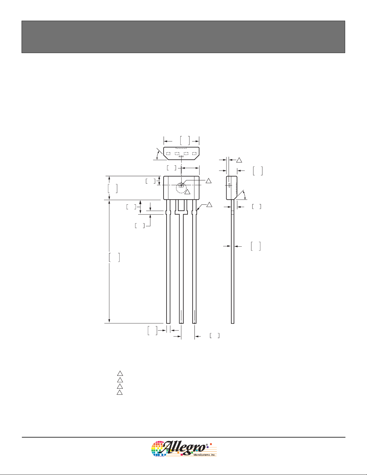
Package KB, 3-Pin SIP
.208
5.28
.203
5.16
45°
.138
.133
3.51
3.38
.085
MAX
2.16
.0520
NOM
BSC
1.32
.1025
NOM
2.60
D
B
A
C
.063
1.60
.059
1.50
45°
BSC
.033
0.84
REF
.020
0.51
REF
.600
15.24
.560
14.22
231
.023
0.58
.018
0.46
Dimensions in inches
Millimeters in brackets, for reference only
Dimensions exclusive of mold flash, gate burrs, or dambar protrusions
Exact case and lead configuration at supplier discretion within limits shown
A
Dambar removal protrusion (6X)
B
Ejector mark on opposite side
C
Active Area Depth .0165 [0.42] NOM
Hall element (not to scale)
D
.075
NOM
1.91
.0173
.0138
0.44
0.35
A1373-DS, Rev. 3
Allegro MicroSystems, Inc.
115 Northeast Cutoff, Box 15036
Worcester, Massachusetts 01615-0036 (508) 853-5000
www.allegromicro.com
22

A1373 and A1374
High Precision, Output Pin Programmable, Linear Hall Effect Sensors
A1373-DS, Rev. 3
The products described herein are manufactured under one or more of
the following U.S. patents: 5,045,920; 5,264,783; 5,442,283; 5,389,889;
5,581,179; 5,517,112; 5,619,137; 5,621,319; 5,650,719; 5,686,894;
5,694,038; 5,729,130; 5,917,320; and other patents pending.
Allegro MicroSystems, Inc. reserves the right to make, from time to
time, such de par tures from the detail spec i fi ca tions as may be required
to permit improvements in the per for mance, reliability, or manufacturability of its products. Before placing an order, the user is cautioned to
verify that the information being relied upon is current.
Allegro products are not authorized for use as critical components in
life-support devices or sys tems without express written approval.
The in for ma tion in clud ed herein is believed to be ac cu rate and reliable.
How ev er, Allegro MicroSystems, Inc. assumes no re spon si bil i ty for its
use; nor for any in fringe ment of patents or other rights of third parties
which may result from its use.
Copyright © 2005, Allegro MicroSystems, Inc.
Allegro MicroSystems, Inc.
115 Northeast Cutoff, Box 15036
Worcester, Massachusetts 01615-0036 (508) 853-5000
www.allegromicro.com
23
 Loading...