

Page 1
查询A1321ELHLT-T供应商
A1321/A1322/A1323
Ratiometric Linear Hall Effect Sensor for High-Temperature Operation
The A132X family of linear Hall-effect sensors are optimized, sensitive, and temperature-stable. These ratiometric Hall-effect sensors provide a voltage output that
is proportional to the applied magnetic fi eld. The A132X family has a quiescent
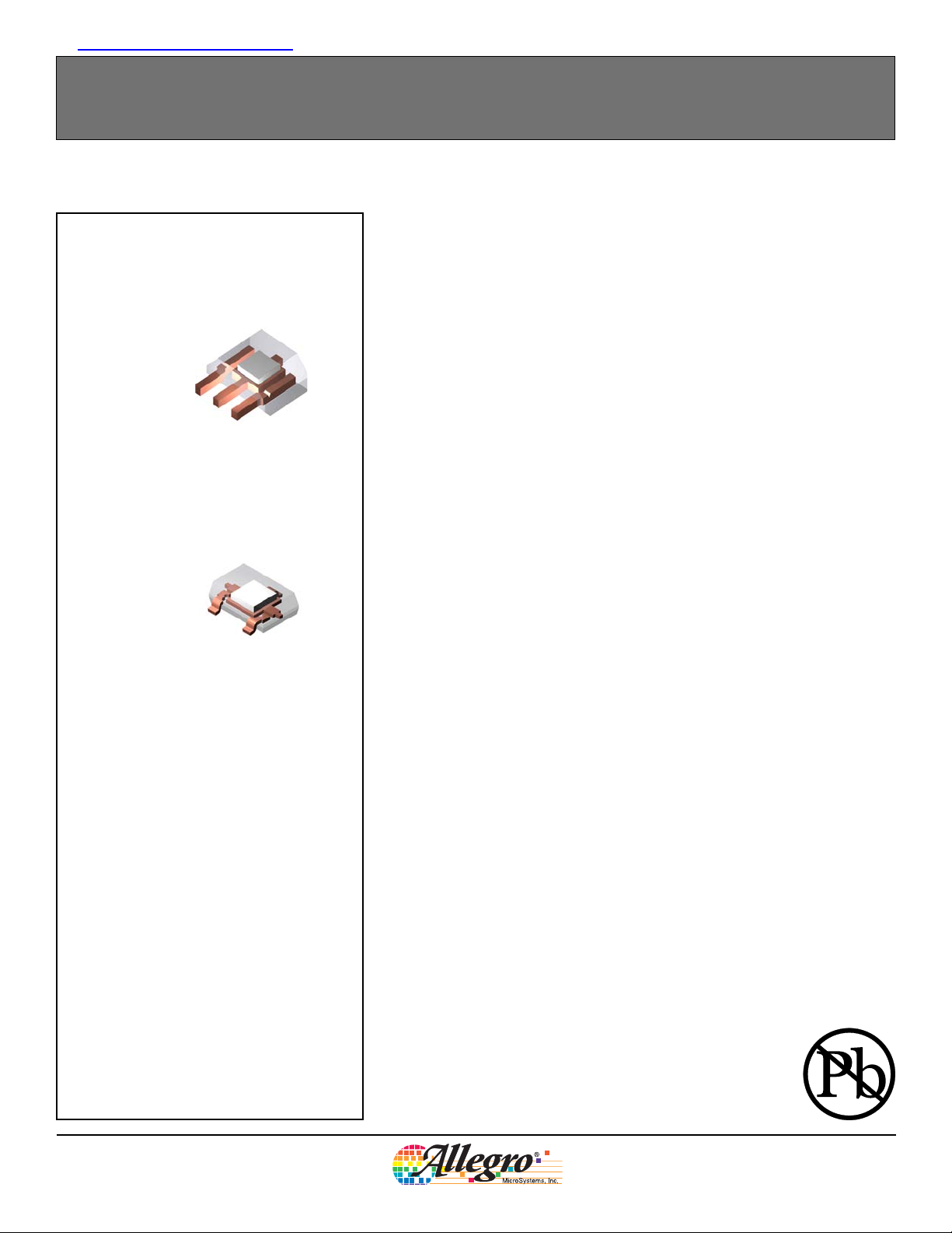
Package UA, 3-pin SIP
1. VCC
2. GND
3. VOUT
1
2
3
Package LH, 3-pin Surface Mount
1. VCC
2. VOUT
3. GND
1
2
3
output voltage that is 50% of the supply voltage and output sensitivity options
of 2.5mV/G, 3.125mV/G, and 5mV/G. The features of this family of devices are
ideal for use in the harsh environments found in automotive and industrial linear
and rotary position sensing systems.
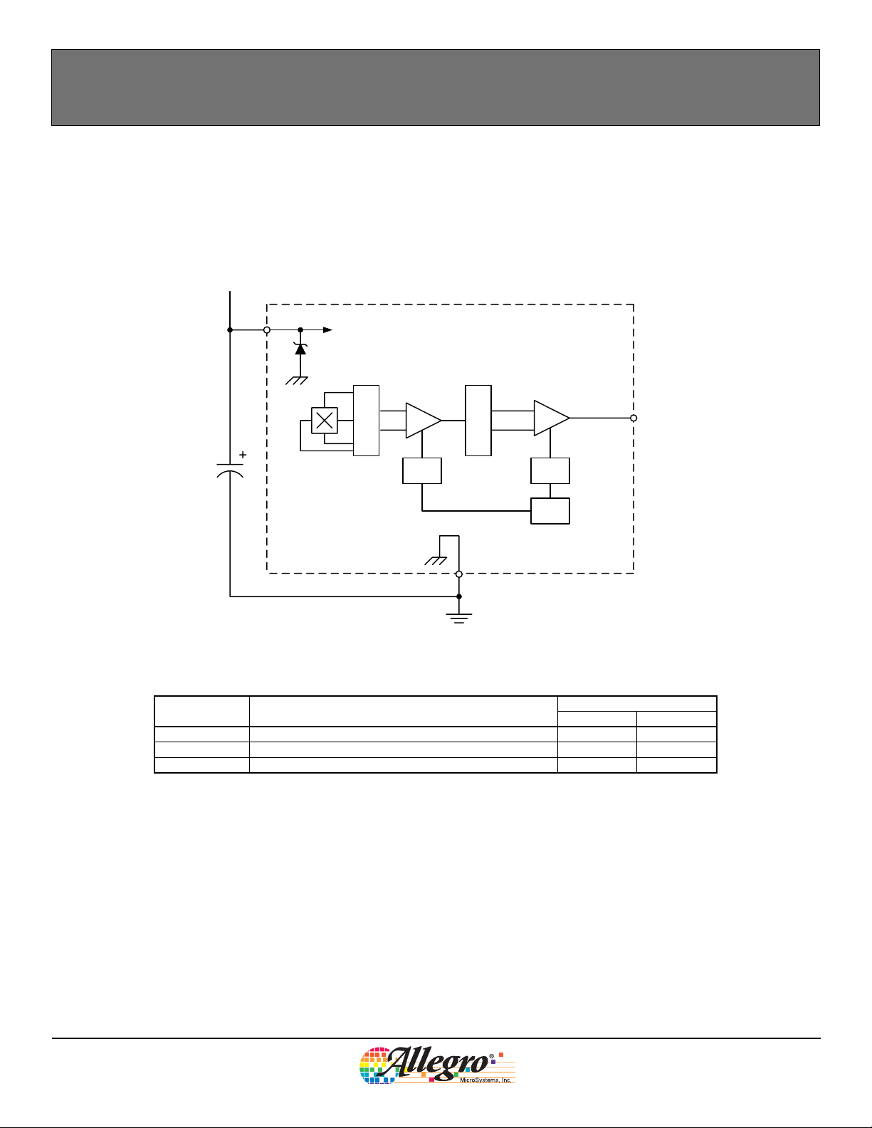
Each device has a BiCMOS monolithic circuit which integrates a Hall element,
improved temperature-compensating circuitry to reduce the intrinsic sensitivity
drift of the Hall element, a small-signal high-gain amplifi er, and a rail-to-rail low-
impedance output stage.
A proprietary dynamic offset cancellation technique, with an internal high-frequency clock, reduces the residual offset voltage normally caused by device
overmolding, temperature dependencies, and thermal stress. The high frequency
clock allows for a greater sampling rate, which results in higher accuracy and
faster signal processing capability. This technique produces devices that have an
extremely stable quiescent output voltage, are immune to mechanical stress, and
have precise recoverability after temperature cycling. Having the Hall element
and an amplifi er on a single chip minimizes many problems normally associated
with low-level analog signals.
Output precision is obtained by internal gain and offset trim adjustments made at
end-of-line during the manufacturing process.
AB SO LUTE MAX I MUM RAT INGS
Supply Voltage, VCC.......................................... 8 V
Reverse-Battery Voltage, V
Reverse-Output Voltage, V
Output Sink Current, I
Operating Temperature
Ambient, T
Ambient, T
Maximum Junction, T
Storage Temperature, T
*
Additional current draw may be observed at voltages
above the minimum supply Zener clamp voltage, V
due to the Zener diode turning on.
OUT
, Range E..................–40ºC to 85ºC
A
, Range L................–40ºC to 150ºC
A
.......................–0.1 V
RCC
.....................–0.1 V
ROUT
............................. 10 mA
........................165ºC
J(max)
..................–65ºC to 170ºC
S
Z(min)
The A132X family is provided in a 3-pin single in-line package (UA) and a 3-pin
surface mount package (LH). Each package is available in a lead (Pb) free version
(suffi x, –T) , with a 100% matte tin plated leadframe.
Features and Benefi ts
Temperature-stable quiescent output voltage
*
Precise recoverability after temperature cycling
Output voltage proportional to magnetic fl ux density
Ratiometric rail-to-rail output
Improved sensitivity
4.5 to 5.5 V operation
Immunity to mechanical stress
Solid-state reliability
Robust EMC protection
,
A1321-DS, Rev. 5
Allegro MicroSystems, Inc.
115 Northeast Cutoff, Box 15036
Worcester, Massachusetts 01615-0036 (508) 853-5000
www.allegromicro.com
Page 2

A1321/A1322/A1323
Ratiometric Linear Hall Effect Sensor for High-Temperature Operation
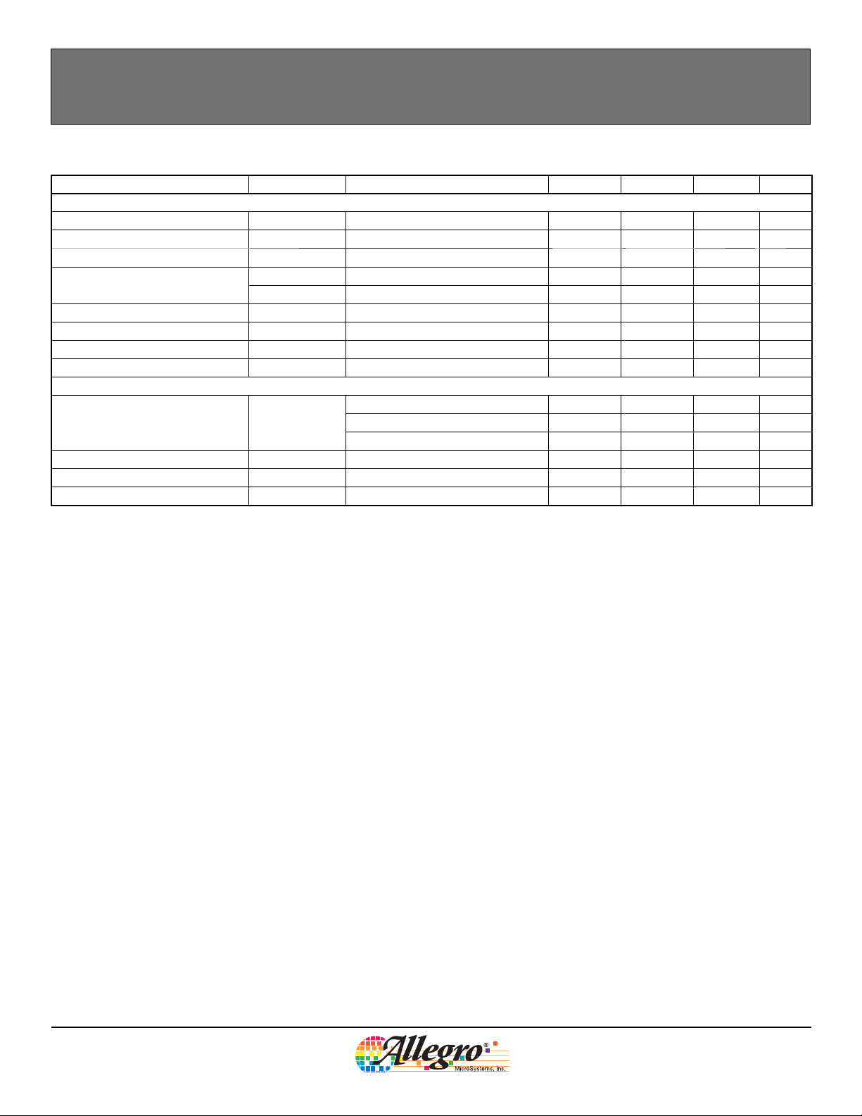
Product Selection Guide
Part Number Pb-free Packing* Mounting
A1321ELHLT –
A1321ELHLT-T Yes
A1321EUA –
A1321EUA-T Yes
A1321LLHLT –
A1321LLHLT-T Yes
A1321LUA –
A1321LUA-T Yes
A1322ELHLT –
A1322ELHLT-T Yes
A1322EUA –
A1322EUA-T Yes
A1322LLHLT –
A1322LLHLT-T Yes
A1322LUA –
A1322LUA-T Yes
A1323ELHLT –
A1323ELHLT-T Yes
A1323EUA –
A1323EUA-T Yes
A1323LLHLT –
A1323LLHLT-T Yes
A1323LUA –
A1323LUA-T Yes
*Contact Allegro for additional packing options.
7-in. reel, 3000 pieces/reel Surface Mount
Bulk, 500 pieces/bag SIP through hole
7-in. reel, 3000 pieces/reel Surface Mount
Bulk, 500 pieces/bag SIP through hole
7-in. reel, 3000 pieces/reel Surface Mount
Bulk, 500 pieces/bag SIP through hole
7-in. reel, 3000 pieces/reel Surface Mount
Bulk, 500 pieces/bag SIP through hole
7-in. reel, 3000 pieces/reel Surface Mount
Bulk, 500 pieces/bag SIP through hole
7-in. reel, 3000 pieces/reel Surface Mount
Bulk, 500 pieces/bag SIP through hole
Ambient, TA
(ºC)
–40 to 85
–40 to 150
–40 to 85
–40 to 150
–40 to 85
–40 to 150
Sensitivity,
Typ. (mV/G)
5.000
3.125
2.500
A1321-DS, Rev. 5
Allegro MicroSystems, Inc.
115 Northeast Cutoff, Box 15036
Worcester, Massachusetts 01615-0036 (508) 853-5000
www.allegromicro.com
2
Page 3
A1321/A1322/A1323
Ratiometric Linear Hall Effect Sensor for High-Temperature Operation
Functional Block Diagram
V+
VCC
Out
Offset
Trim
Control
0.1 μF
Amp
Cancellation
Dynamic Offset
Gain
Filter
GND
Terminal List
Symbol Description
Package LH Package UA
Number
VCC Connects power supply to chip 1 1
VOUT Output from circuit 2 3
GND Ground 3 2
VOUT
A1321-DS, Rev. 5
Allegro MicroSystems, Inc.
115 Northeast Cutoff, Box 15036
Worcester, Massachusetts 01615-0036 (508) 853-5000
www.allegromicro.com
3
Page 4
A1321/A1322/A1323
Ratiometric Linear Hall Effect Sensor for High-Temperature Operation
DEVICE CHARACTERISTICS
Characteristic Symbol Test Conditions Min. Typ.
Electrical Characteristics; V
Supply Voltage V
Supply Current I
Quiescent Voltage V
Output Voltage
3
Output Source Current Limit
Supply Zener Clamp Voltage V
1
over operating temperature (TA) range, unless otherwise noted
= 5 V, unless otherwise noted
CC
cc(op)
cc
out(q)
V
out(H)
V
3
out(L)
I
out(LM)
Z
Operating; Tj < 165°C 4.5 5.0 5.5 V
B = 0, I
B = 0, TA = 25ºC, I
B = +X, I
B = –X, I
B = –X, V
Icc = 11 mA = I
= 0 – 5.6 8 mA
out
= 1 mA 2.425 2.5 2.575 V
out
= –1 mA – 4.7 – V
out
= 1 mA – 0.2 – V
out
→ 0 –1.0 –1.5 – mA
out
+ 3 6 8.3 – V
cc(max)
2
Max. Units
Output Bandwidth BW – 30 – kHz
Clock Frequency f
Output Characteristics; over V
Noise, Peak-to-Peak
4
range, unless otherwise noted
CC
Output Resistance R
Output Load Resistance R
Output Load Capacitance C
1
Negative current is defi ned as conventional current coming out of (sourced from) the specifi ed device terminal.
2
Typical data is at TA = 25°C. They are for initial design estimations only, and assume optimum manufacturing and application
C
A1321; C
V
N
A1322; C
A1323; C
I
out
L
L
≤ ±1 mA – 1.5 3 Ω
out
I
≤ ±1 mA, VOUT to GND 4.7 – – kΩ
out
VOUT to GND – – 10 nF
= 0.1 μF, no load – – 40 mV
bypass
= 0.1 μF, no load – – 25 mV
bypass
= 0.1 μF, no load – – 20 mV
bypass
– 150 – kHz
conditions. Performance may vary for individual units, within the specifi ed maximum and minimum limits.
3
In these tests, the vector X is intended to represent positive and negative fi elds suffi cient to swing the output driver between fully OFF
and saturated (ON), respectively. It is NOT intended to indicate a range of linear operation.
4
Noise specifi cation includes both digital and analog noise.
A1321-DS, Rev. 5
Allegro MicroSystems, Inc.
115 Northeast Cutoff, Box 15036
Worcester, Massachusetts 01615-0036 (508) 853-5000
www.allegromicro.com
4
Page 5

A1321/A1322/A1323
Ratiometric Linear Hall Effect Sensor for High-Temperature Operation
MAGNETIC CHARACTERISTICS
Characteristics Symbol Test Condition Min Typ
1,2
over operating temperature range, TA; VCC = 5 V, I
= –1 mA; unless otherwise noted
out
3
Max Units
4
A1321; TA = 25ºC 4.750 5.000 5.250 mV/G
Sensitivity
5
Sens
A1322; TA = 25ºC 2.969 3.125 3.281 mV/G
A1323; TA = 25ºC 2.375 2.500 2.625 mV/G
out(q)
as a func-
out(q)
V
out(q)(ΔT)
V
out(q)(ΔV)
Defi ned in terms of magnetic fl ux density, B – – ±10 G
– – ±1.5 %
(ΔV)
– – ±1.5 %
Delta V
tion of temperature
Ratiometry, V
Ratiometry, Sens ΔSens
Positive Linearity Lin+ – – ±1.5 %
Negative Linearity Lin– – – ±1.5 %
Symmetry Sym – – ±1.5 %
UA Package
Delta Sens at T
Delta Sens at TA = min5ΔSens
Sensitivity Drift
= max5ΔSens
A
6
Sens
(TAmax)
(TAmin)
Drift
From hot to room temperature –2.5 – 7.5 %
From cold to room temperature –6 – 4 %
TA = 25°C; after temperature cycling and over time – 1 2 %
LH Package
Delta Sens at TA = max5ΔSens
Delta Sens at TA = min5ΔSens
Sensitivity Drift
1
Additional information on chracteristics is provided in the section Characteristics Defi nitions, on the next page.
2
Negative current is defi ned as conventional current coming out of (sourced from) the specifi ed device terminal.
3
Typical data is at T
6
= 25°C, except for ΔSens, and at x.x Sens. Typical data are for initial design estimations only, and assume optimum
A
(TAmax)
(TAmin)
Sens
From hot to room temperature –5 – 5 %
From cold to room temperature –3.5 – 8.5 %
TA = 25°C; after temperature cycling and over time – 0.328 2 %
Drift
manufacturing and application conditions. Performance may vary for individual units, within the specifi ed maximum and minimum limits.
In addition, the typical values vary with gain.
4
10 G = 1 millitesla.
5
After 150ºC pre-bake and factory programming.
6
Sensitivity drift is the amount of recovery with time.
A1321-DS, Rev. 5
Allegro MicroSystems, Inc.
115 Northeast Cutoff, Box 15036
Worcester, Massachusetts 01615-0036 (508) 853-5000
www.allegromicro.com
5
Page 6

A1321/A1322/A1323
V
out(q)(VCC)Vout(q)(5V)
ΔV
out(q)(ΔV)
=
× 100%
VCC5V
VCC5V
=
× 100%
ΔSens
(ΔV)
Sens
(VCC)
Sens
(5V)
–
=
× 100%
Lin+
V
out(+B)
2(V
out(+B / 2)–Vout(q)
)
V
out(q)
–
=
× 100%
Lin–
V
out(–B)
2(V
out(–B / 2)–Vout(q)
)
V
out(q)
–
=
× 100%
Sym
V
out(+B)
V
out(q)–Vout(–B)
V
out(q)
Ratiometric Linear Hall Effect Sensor for High-Temperature Operation
Characteristic Defi nitions
Quiescent Voltage Output. In the quiescent state (no
magnetic fi eld), the output equals one half of the supply voltage
over the operating voltage range and the operating temperature
range. Due to internal component tolerances and thermal considerations, there is a tolerance on the quiescent voltage output
both as a function of supply voltage and as a function of ambient
temperature. For purposes of specifi cation, the quiescent voltage
output as a function of temperature is defi ned in terms of mag-
netic fl ux density, B, as:
(1)
ΔV
out(q)(ΔΤ)
V
out(q)(ΤΑ)Vout(q)(25ºC)
=
Sens
–
(25ºC)
This calculation yields the device’s equivalent accuracy,
over the operating temperature range, in gauss (G).
Sensitivity. The presence of a south-pole magnetic fi eld per-
pendicular to the package face (the branded surface) increases
the output voltage from its quiescent value toward the supply
voltage rail by an amount proportional to the magnetic fi eld
applied. Conversely, the application of a north pole will decrease
the output voltage from its quiescent value. This proportionality
is specifi ed as the sensitivity of the device and is defi ned as:
(2)
Sens
V
out(–B)Vout(+B)
=
–
2B
Ratiometric. The A132X family features a ratiometric output.
The quiescent voltage output and sensitivity are proportional to
the supply voltage (ratiometric).
The percent ratiometric change in the quiescent voltage output is
defi ned as:
(4)
and the percent ratiometric change in sensitivity is
defi ned as:
(5)
Linearity and Symmetry. The on-chip output stage
is designed to provide a linear output with a supply voltage of
5 V. Although application of very high magnetic fi elds will not
damage these devices, it will force the output into a non-linear
region. Linearity in percent is measured and defi ned as:
(6)
(7)
The stability of sensitivity as a function of temperature is
defi ned as:
A1321-DS, Rev. 5
ΔSens
(ΔΤ)
=
Sens
(ΤΑ)
Sens
Sens
–
(25ºC)
(25ºC)
× 100%
(3)
and output symmetry as:
(8)
Allegro MicroSystems, Inc.
115 Northeast Cutoff, Box 15036
Worcester, Massachusetts 01615-0036 (508) 853-5000
www.allegromicro.com
6
Page 7

A1321/A1322/A1323
Average Supply Current (ICC) vs Temperature
Vcc=5V
0
0.5
1
1.5
2
2.5
3
3.5
4
4.5
5
5.5
6
6.5
7
7.5
8
-40
-20
0
25
85
115
125
150
TA(°C)
I
CC
(mA)
Average Positive Linearity (Lin+) vs Temperature
V
cc
=5V
95
96
97
98
99
100
101
102
103
104
105
-40
-20
0
25
85
115
125
150
TA(°C)
Lin+ (%)
Average Negative Linearity (Lin–) vs Temperature
V
cc
=5V
95
96
97
98
99
100
101
102
103
104
105
-40
-20
0
25
85
115
125
150
TA(°C)
Lin
–
(%)
Average Ratiometry, V
OUT(q)(ΔV)
vs Temperature
99
99.2
99.4
99.6
99.8
100
100.2
100.4
100.6
100.8
101
-40
-20
0
25
85
115
125
150
TA(°C)
Ratiometry (%)
4.5 to 5.0 V
5.5 to 5.0 V
Average Ratiometry, ΔSens
(ΔV),
vs Temperature
99
99.2
99.4
99.6
99.8
100
100.2
100.4
100.6
100.8
101
-40
-20
0
25
85
115
125
150
TA(°C)
Ratiometry (%)
4.5 to 5.0V
5.5 to 5.0V
Ratiometric Linear Hall Effect Sensor for High-Temperature Operation
Typical Characteristics
(30 pieces, 3 fabrication lots)
Continued on the next page...
A1321-DS, Rev. 5
Allegro MicroSystems, Inc.
115 Northeast Cutoff, Box 15036
Worcester, Massachusetts 01615-0036 (508) 853-5000
www.allegromicro.com
7
Page 8

A1321/A1322/A1323
Average Absolute Quiescent Output Voltage, V
out(q)
,vsTemperature
Vcc=5V
2.425
2.45
2.475
2.5
2.525
2.55
2.575
-40
-20
0
25
85
115
125
150
TA(°C)
V
out(q)
(V)
Average Absolute Sensitivity, Sens, vs Temperature
Vcc=5V
2
2.5
3
3.5
4
4.5
5
5.5
6
-40
-20
0
25
85
115
125
150
TA(°C)
Sens (mV/G)
A1322
A1321
A1323
Average Delta Quiescent Output Voltage, V
out(q)(ΔT)
,
vs Temperature
Δ in
readings at each temperature are relative to 25°C
Vcc=5V
-10
-8
-6
-4
-2
0
2
4
6
8
10
-40
-20
0
25
85
115
125
150
TA(°C)
V
out(q)(ΔT)
(G)
Quiescent Output Voltage, V
out(q)
,vsV
cc
T
A
=25°C
2
2.1
2.2
2.3
2.4
2.5
2.6
2.7
2.8
2.9
3
4.5 5 5.5
Vcc(V)
V
out(q)
(V)
1321
1322
1323
Average Sensitivity, Sens, vs V
cc
T
A
=25°C
1
1.5
2
2.5
3
3.5
4
4.5
5
5.5
6
4.5 5 5.5
Vcc(V)
Sens (mV/G)
1321
1322
1323
Average Delta Sensitivity, ΔSens, vs Temperature
Δ in readings at each temperature are relative to 25°C
V
cc
=5V
-10
-8
-6
-4
-2
0
2
4
6
8
10
-40
-20
0
25
85
115
125
150
TA(°C)
ΔSens
(%)
Ratiometric Linear Hall Effect Sensor for High-Temperature Operation
Typical Characteristics, continued
(30 pieces, 3 fabrication lots)
A1321-DS, Rev. 5
Allegro MicroSystems, Inc.
115 Northeast Cutoff, Box 15036
Worcester, Massachusetts 01615-0036 (508) 853-5000
www.allegromicro.com
8
Page 9

3.00
2.70
A1321/A1322/A1323
Ratiometric Linear Hall Effect Sensor for High-Temperature Operation
Package LH, 3-Pin; (SOT-23W)
3.10
.122
2.90
.114
1.49
.118
.106
2.10
1.85
.083
.073
0.55
REF
0.96
.038
NOM
0.50 .020
0.30
.012
.022
.059
3
A
NOM
0.28
.011
NOM
21
1.13
0.87
0.95
BSC
.037
0.15
0.00
.006
.000
.045
.034
8º
0º
0.20
0.13
0.25
MIN
0.25
.010
BSC
Seating Plane
Gauge Plane
.008
.005
.010
1.00
BSC
.039
0.70
.028
BSC
A
B
C
C
Dimensions in millimeters
U.S. Customary dimensions (in.) in brackets, for reference only
Hall element
Active Area Depth 0.28 [.011]
Fits SC–59A Solder Pad Layout
2.40
BSC
0.95
BSC
.094
.037
.122
.117
3.10
2.97
.640
.600
16.26
15.24
.0565
NOM
.085
MAX
Package UA, 3-Pin
.164
4.17
.159
4.04
45°
BSC
.0805
2.04
NOM
1.44
B
2.16
A
231
.019
0.48
.014
0.36
Dimensions in inches
Metric dimensions (mm) in brackets, for reference only
A
Dambar removal protrusion
B
Hall element
.050
BSC
.062
.058
1.27
.031
REF
.017
.014
1.57
1.47
0.79
0.44
0.35
.0195
NOM
0.50
45°
BSC
A1321-DS, Rev. 5
Allegro MicroSystems, Inc.
115 Northeast Cutoff, Box 15036
Worcester, Massachusetts 01615-0036 (508) 853-5000
www.allegromicro.com
9
Page 10

A1321/A1322/A1323
Ratiometric Linear Hall Effect Sensor for High-Temperature Operation
A1321-DS, Rev. 5
The products described herein are manufactured under one
or more of the following U.S. patents: 5,045,920; 5,264,783;
5,442,283; 5,389,889; 5,581,179; 5,517,112; 5,619,137; 5,621,319;
5,650,719; 5,686,894; 5,694,038; 5,729,130; 5,917,320; and other
patents pending.
Allegro MicroSystems, Inc. reserves the right to make, from time
to time, such de par tures from the detail spec i fi ca tions as may be
required to permit improvements in the per for mance, reliability,
or manufacturability of its products. Before placing an order, the
user is cautioned to verify that the information being relied upon is
current.
Allegro products are not authorized for use as critical components in life-support devices or sys tems without express written
approval.
The in for ma tion in clud ed herein is believed to be ac cu rate and
reliable. How ev er, Allegro MicroSystems, Inc. assumes no re spon si bil i ty for its use; nor for any in fringe ment of patents or other
rights of third parties which may result from its use.
Copyright © 2004, 2005, Allegro MicroSystems, Inc.
Allegro MicroSystems, Inc.
115 Northeast Cutoff, Box 15036
Worcester, Massachusetts 01615-0036 (508) 853-5000
www.allegromicro.com
10
Page 11

 Loading...