

ALLEGRO A1185, A1186 User Manual
A1185 and A1186
Ultrasensitive T wo-Wire Field-Programmable
Chopper-Stabilized Unipolar Hall-Effect Switches
Features and Benefits
▪ Chopper stabilization
▫ Low switchpoint drift over operating
temperature range
▫ Low sensitivity to stress
▪ Field programmable for optimized switchpoints
▪ On-chip protection
▫ Supply transient protection
▫ Reverse-battery protection
▫ On-board voltage regulator
▫ 3.5 to 24 V operation
Packages: 3 pin SOT23W (suffix LH), and
3 pin SIP (suffix UA)
Description
The A1185 and A1186 are ultrasensitive, two-wire, unipolar
Hall effect switches. The operate point, BOP, can be fieldprogrammed, after final packaging of the sensor and
placement into the application. This advanced feature allows
the optimization of the sensor switching performance, by
effectively accounting for variations caused by mounting
tolerances for the device and the target magnet.
This family of devices are produced on the Allegro
MicroSystems new DABIC5 BiCMOS wafer fabrication
process, which implements a patented, high-frequency, chopperstabilization technique that achieves magnetic stability and
eliminates the offsets that are inherent in single-element devices
exposed to harsh application environments. Commonly found
in a number of automotive applications, the A1185 and A1186
devices are utilized to sense: seat track position, seat belt buckle
presence, hood/trunk latching, and shift selector position.
Two-wire unipolar switches are particularly advantageous
in price-sensitive applications, because they require one less
wire than the more traditional open-collector output switches.
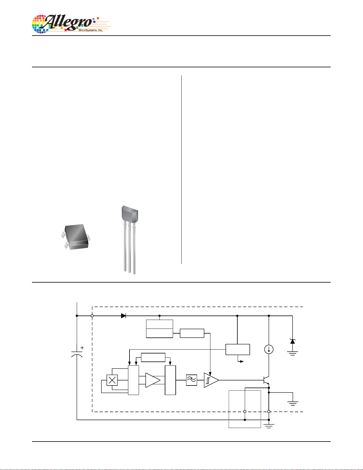
Not to scale
V+
VCC
0.01 uF
Continued on the next page…
Functional Block Diagram
Program/Lock
Dynamic Offset
Cancellation
Programming
Logic
Clock/Logic
Amp
Offset
Adjust
Low-Pass
Filter
Sample and Hold
Regulator
To all
subcircuits
GND
Package UA Only
GND
A1185-DS, Rev. 2
A1185 and
Ultrasensitive T wo-Wire Field-Programmable
A1186
Chopper-Stabilized Unipolar Hall Effect Switches
Description (continued)
Additionally, the system designer gains inherent diagnostics
because output current normally flows in either of two narrowlyspecified ranges. This provides distinct current ranges for I
and I
. Any output current level outside of these two ranges
OUT(L)
OUT(H)
is a fault condition.
Other features of the A1185 and A1186 devices include on-chip
transient protection and a Zener clamp on the power supply to protect
against overvoltage conditions on the supply line.
present. The A1185 has an inverted output current level: switching
LOW in the presence of a south polarity magnetic field of sufficient
strength, and HIGH otherwise.
Both devices are offered in two package styles: LH, a SOT-23W
miniature low-profile package for surface-mount applications, and
UA, a three-lead ultramini Single Inline Package (SIP) for throughhole mounting. Each package is available in a lead (Pb) free version
(suffix, –T) with 100% matte tin plated leadframe.
The output current of the A1186 switches
a south polarity magnetic field of sufficient strength; and switches
LOW otherwise, including when there is no significant magnetic field
HIGH in the presence of
Factory-programmed versions are also available. Refer to: A1145
and A1146.
Selection Guide
Part Number Pb-free
A1185ELHLT-T Yes 7-in. reel, 3000 pieces/reel Surface mount
A1185EUA-T Yes Bulk, 500 pieces/bag 4-pin SIP through hole
A1185LLHLT-T Yes 7-in. reel, 3000 pieces/reel Surface mount
A1185LUA-T Yes Bulk, 500 pieces/bag 4-pin SIP through hole
A1186ELHLT-T Yes 7-in. reel, 3000 pieces/reel Surface mount
A1186EUA-T Yes Bulk, 500 pieces/bag 4-pin SIP through hole
A1186LLHLT-T Yes 7-in. reel, 3000 pieces/reel Surface mount
A1186LUA-T Yes Bulk, 500 pieces/bag 4-pin SIP through hole
1
Pb-based variants are being phased out of the product line. Certain variants cited in this footnote are in production but have been determined to be NOT FOR NEW
DESIGN. This classification indicates that sale of this device is currently restricted to existing customer applications. The device should not be purchased for new design
applications because obsolescence in the near future is probable. Samples are no longer available. Status change: May 1, 2006. These variants include: A1185ELHLT,
A1185EUA, A1185LLHLT, A1185LUA, A1186ELHLT, A1186EUA, A1186LLHLT, and A1186LUA.
2
Contact Allegro for additional packing options.
3
South (+) magnetic fields must be of sufficient strength.
1
Packing
2
Mounting
Ambient, T
–40 to 85
–40 to 150
–40 to 85
–40 to 150
(°C)
A
Output
South (+) Field
Low
High
Supply Current at Low
3
Output, I
5 to 6.9
(mA)
CC(L)
Absolute Maximum Ratings
Characteristic Symbol Notes Rating Units
Supply Voltage V
Reverse Supply Voltage V
Magnetic Flux Density B Unlimited G
Operating Ambient Temperature T
Maximum Junction Temperature T
Storage Temperature T
CC
RCC
A
(max) 165 ºC
J
stg
Range E –40 to 85 ºC
Range L –40 to 150 ºC
28 V
–18 V
–65 to 170 ºC
Allegro MicroSystems, Inc.
115 Northeast Cutoff, Box 15036
Worcester, Massachusetts 01615-0036 (508) 853-5000
www.allegromicro.com
2
A1185 and
Ultrasensitive T wo-Wire Field-Programmable
A1186
Chopper-Stabilized Unipolar Hall Effect Switches
ELECTRICAL CHARACTERISTICS over the operating voltage and temperature ranges, unless otherwise specified
Characteristic Symbol Test Conditions Min. Typ. Max. Units
= I
1
2
4
5
6,7
CCL(max)
+ 3 mA.
V
CC
I
CC(L)
I
CC(H)
ZSupplyICC
3
I
ZSupply
RCC
Device powered on 3.5 – 24 V
B >BOP for A1185; B <BRP for A1186 5 – 6.9 mA
B >BOP for A1186; B <BRP for A1185 12 – 17 mA
= I
CC(L)(Max)
V
= 28 V – – 9.9 mA
Supply
V
= –18 V – – 1.6 mA
RCC
+ 3 mA; TA = 25°C 28 – 40 V
No bypass capacitor; capacitance of the
di/dt
oscilloscope performing the measurement
– 36 – mA/μs
= 20 pF
C
t
on
After factory trimming; with and without
bypass capacitor (C
POS ton ≤ t
on(max)
= 0.01 μF)
BYP
; V
slew rate > 25 mV/μs – HIGH – –
CC
– 200 – kHz
––25μs
Supply Voltage
Supply Current
Supply Zener Clamp Voltage V
Supply Zener Clamp Current
Reverse Supply Current I
Output Slew Rate
Chopping Frequency f
Power-On Time
Power-On State
1
VCC represents the generated voltage between the VCC pin and the GND pin.
2
Relative values of B use the algebraic convention, where positive values indicate south magnetic polarity, and negative values indicate north magnetic
polarity; therefore greater B values indicate a stronger south polarity field (or a weaker north polarity field, if present).
3
I
ZSUPPLY(max)
4
Measured without bypass capacitor between VCC and GND. Use of a bypass capacitor results in slower current change.
5Measured with and without bypass capacitor of 0.01 μF. Adding a larger bypass capacitor causes longer Power-On Time.
6
POS is defined as true only with a VCC slew rate of 25 mV / μs or greater. Operation with a VCC slew rate less than 25 mV / μs can permanently harm
device performance.
7
POS is undefined for t > ton or BRP < B < BOP .
MAGNETIC CHARACTERISTICS
1
over the operating voltage and temperature ranges, unless otherwise specified
Characteristic Symbol Test Conditions Min. Typ. Max. Units
Programmable Operate Point Range B
Initial Operate Point Range B
Switchpoint Step Size
2
OPrange
OPinitVCC
B
RES
ICC = I
ICC = I
VCC = 5 V, TA = 25°C 2 4 6 G
for A1185
CC(L)
CC(H)
for A1186
10 – 60 G
= 12 V – –10 10 G
Switchpoint setting – 5 – Bit
Number of Programming Bits
Temperature Drift of B
OP
Hysteresis B
1
Relative values of B use the algebraic convention, where positive values indicate south magnetic polarity, and negative values indicate north magnetic
polarity; therefore greater B values indicate a stronger south polarity field (or a weaker north polarity field, if present).
2
The range of values specified for B
is a maximum, derived from the cumulative programming bit errors.
RES
ΔB
–
Programming locking – 1 – Bit
OP
HYS
B
HYS
= BOP – B
RP
– – ±20 G
51530G
Allegro MicroSystems, Inc.
115 Northeast Cutoff, Box 15036
Worcester, Massachusetts 01615-0036 (508) 853-5000
www.allegromicro.com
3
A1185 and
Ultrasensitive T wo-Wire Field-Programmable
A1186
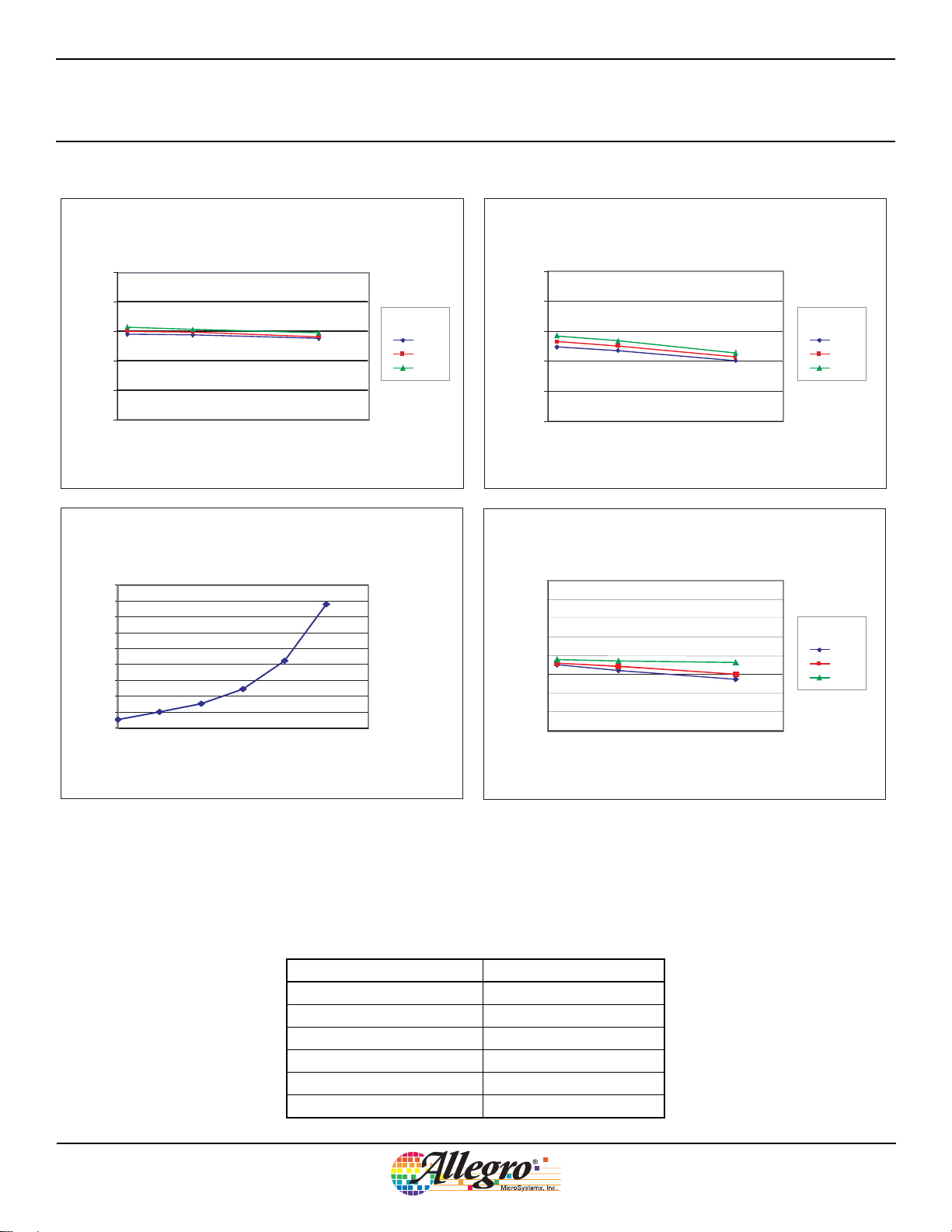
10
8
6
(mA)
4
CC(L)
I
2
0
-50 0 50 100 150 200
70
60
50
40
30
(G)
20
OP
B
10
0
–10
–20
01234 65
Chopper-Stabilized Unipolar Hall Effect Switches
Characteristic Data
I
versus Ambient Temperature
CC(L)
at Various Levels of V
CC
(A1185 and A1186)
20
(mA)
CC(H)
I
18
16
14
12
10
VCC(V)
3.5
12.0
24.0
Ambient Temperature, TA(°C) Ambient Temperature, TA(°C)
BOPSet by Specific Programming Bit
V
=12V TA= 25°C
CC
(A1185 and A1186)
(G)
HYS
B
Bit Number
I
versus Ambient Temperature
CC(H)
at Various Levels of V
(A1185 and A1186)
-50 0 50 100 150 200
Hysteresis versus Ambient Temperature
at Various Levels of V
(A1185 and A1186)
40
35
30
25
20
15
10
5
-50 0 50 100 150 200
Ambient Temperature, TA(°C)
CC
VCC(V)
3.5
12.0
24.0
CC
VCC(V)
3.5
12.0
24.0
Device Qualification Program
Contact Allegro for information.
EMC (Electromagnetic Compatibility) Requirements
Contact your local representative for EMC results.
Test Name Reference Specification
ESD – Human Body Model AEC-Q100-002
ESD – Machine Model AEC-Q100-003
Conducted Transients ISO 7637-2
Direct RF Injection ISO 11452-7
Bulk Current Injection ISO 11452-4
TEM Cell ISO 11452-3
Allegro MicroSystems, Inc.
115 Northeast Cutoff, Box 15036
Worcester, Massachusetts 01615-0036 (508) 853-5000
www.allegromicro.com
4
A1185 and
Ultrasensitive T wo-Wire Field-Programmable
A1186
Chopper-Stabilized Unipolar Hall Effect Switches
THERMAL CHARACTERISTICS may require derating at maximum conditions, see application information
Characteristic Symbol Test Conditions* Value Units
Package LH, 1-layer PCB with copper limited to solder pads 228 ºC/W
Package Thermal Resistance
R
θJA
Package LH, 2-layer PCB with 0.463 in.
connected by thermal vias
Package UA, 1-layer PCB with copper limited to solder pads 165 ºC/W
*Additional thermal information available on Allegro Web site.
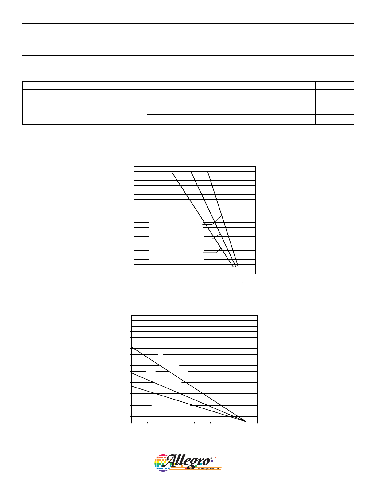
Power Derating Curve
25
24
23
22
21
(V)
20
CC
19
18
17
16
15
14
13
12
11
10
9
Maximum Allowable V
8
7
6
5
4
3
2
2-layer PCB, Package LH
(R
= 110 ºC/W)
θJA
1-layer PCB, Package UA
(R
= 165 ºC/W)
θJA
1-layer PCB, Package LH
(R
= 228 ºC/W)
θJA
20 40 60 80 100 120 140 160 180
Temperature (ºC)
2
of copper area each side
V
CC(max)
V
CC(min)
110 ºC/W
Power Dissipation versus Ambient Temperature
1900
1800
1700
1600
1500
1400
1300
(mW)
D
Power Dissipation, P
1200
1100
1000
900
800
700
600
500
400
300
200
2-layer PCB, Package LH
(R
θJA
= 110 ºC/W)
1-layer
(R
PCB, Pa
θ
JA
= 165 ºC/W)
1-lay
e
rP
(R
θ
J
=
A
22
ckage
UA
CB, Package LH
8ºC
/
W
)
100
0
20 40 60 80 100 120 140 160 180
Temperature (°C)
Allegro MicroSystems, Inc.
115 Northeast Cutoff, Box 15036
Worcester, Massachusetts 01615-0036 (508) 853-5000
www.allegromicro.com
5
 Loading...