

ALLEGRO 6810 DATA SHEET
A6810xA
OUT
1
OUT
8
2
OUT
7
3
OUT
CLOCK
GROUND
LOGIC
SUPPLY
STROBE
OUT
OUT
6
CLK
4
5
6
V
7
ST
8
5
4
LATCHES
REGISTER
REGISTER
LATCHES
DD
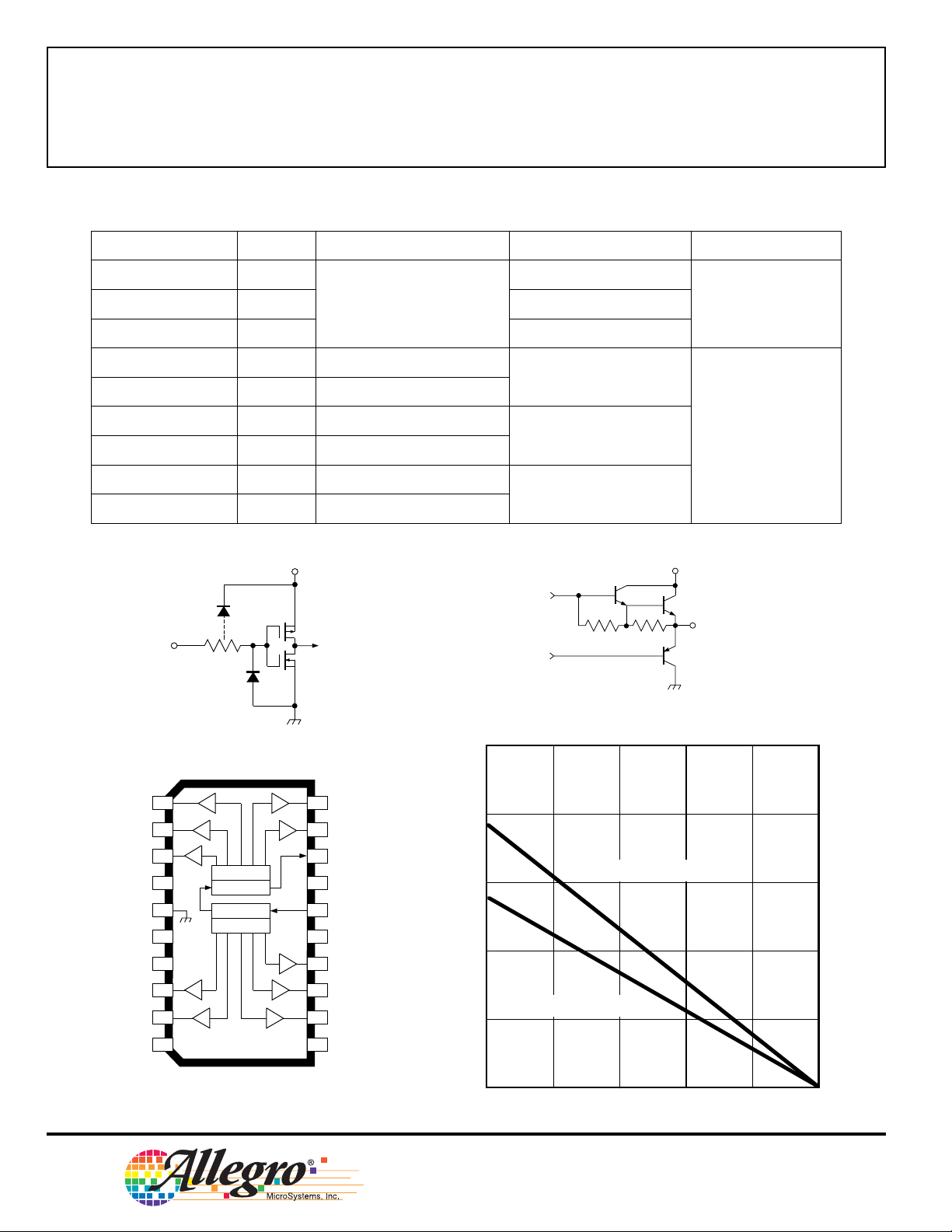
ABSOLUTE MAXIMUM RATINGS
at TA = 25°C
Logic Supply Voltage, V
Driver Supply Voltage, V
Continuous Output Current Range,
I
........................ -40 mA to +15 mA
OUT
Input Voltage Range,
V
....................... -0.3 V to V
IN
Package Power Dissipation,
P
....................................... See Graph
D
Operating Temperature Range, T
(Suffi x ‘E–’) ................... -40°C to +85°C
(Suffi x ‘K–’) ................. -40°C to +125°C
(Suffi x ‘S–’) ................... -20°C to +85°C
Storage Temperature Range,
T
............................... -55°C to +125°C
S
Caution: These CMOS devices have input
static protection (Class 2) but are still susceptible to damage if exposed to extremely
high static electrical charges.
DD
BB
18
9
17
OUT
10
SERIAL
16
DATA OUT
LOAD
V
15
BB
SUPPLY
SERIAL
14
DATA IN
13
12
11
019
BLANKING
OUT
1
OUT
2
OUT
3
Dwg. PP-029
BLNK
.................. 7.0 V
................... 60 V
+ 0.3 V
DD
A
26182.124E
Data Sheet
6810
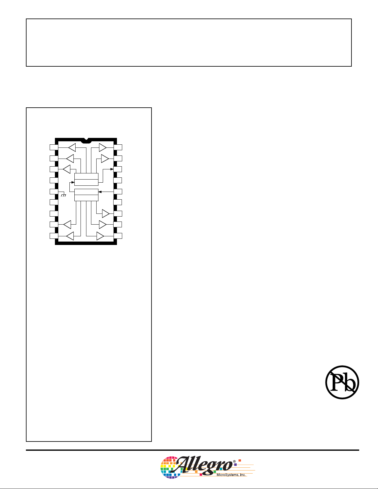
DABiC-IV, 10-BIT SERIAL-INPUT,
LATCHED SOURCE DRIVER
The A6810– devices combine 10-bit CMOS shift registers, ac com pa ny ing data latches and control cir cuit ry with bipolar sourcing out puts
and pnp active pull downs. De signed pri mar ily to drive vacuum-fl u o -
res cent displays, the 60 V and -40 mA output ratings also allow these
devices to be used in many other peripheral power driver ap pli ca tions.
The A6810– feature an increased data input rate (com pared with the
older UCN/UCQ5810-F) and a con trolled output slew rate.
The CMOS shift register and latches allow direct interfacing with
microprocessor-based systems. With a 3.3 V or 5 V logic supply, serialdata input rates of at least 10 MHz .
A CMOS serial data output permits cascade con nec tions in ap pli ca tions re quir ing additional drive lines. Similar devices are available as
the A6812– (20 bits) and A6818– (32 bits).
The A6810– output source drivers are npn Dar ling tons, capable of
sourcing up to 40 mA. The controlled output slew rate reduces elec tro mag net ic noise, which is an important consideration in systems that include telecommunications and/or microprocessors and to meet government emissions regulations. For inter-digit blanking, all output drivers
can be dis abled and all sink drivers turned on with a BLANK ING input
high. The pnp active pull-downs will sink at least
2.5 mA.
The A6810– are available in three temperature ranges for op ti mum
per for mance in commercial (suffi x S-), industrial (suffi x E-), or au-
tomtoive (suffi x K–) ap pli ca tions. They are provided in two package
styles for through-hole DIP (suffi x -A) or minimum-area surface-mount
SOIC (suffi x -LW). Copper lead frames, low logic-power dis si pa tion,
and low output-saturation voltages allow all devices to source 25 mA
from all outputs continuously over the max i mum operating tem pera ture
range.
The lead (Pb) free versions are provided with 100% matte tin
leadframe plating.
FEATURES
■ Controlled Output Slew Rate
■ High-Speed Data Storage
■ 60 V Minimum Output Breakdown
■ High Data Input Rate
■ PNP Active Pull-Downs
■ Low Output-Saturation Voltages
■ Low-Power CMOS Logic and Latches
■ Improved Replacements for TL4810–, UCN5810–, and UCQ5810–
6810
10-BIT SERIAL-INPUT,
LATCHED SOURCE DRIVER
PRODUCT SELECTION GUIDE
Part Number Pb-free Packing
A6810SA
A6810SA-T
A6810EA
A6810EA-T
A6810KA
A6810KA-T
A6810SLW
A6810SLW-T
A6810SLWTR
A6810SLWTR-T
A6810ELW
A6810ELW-T
A6810ELWTR
A6810ELWTR-T
A6810KLW
A6810KLW-T
A6810KLWTR
A6810KLWTR-T
Yes
Yes
Yes
Yes
Yes
Yes
Yes
Yes
Yes
–
–
–
–
–
1000 pieces/13-in. reel
–
–
1000 pieces/13-in. reel
–
–
1000 pieces/13-in. reel
TIUCRICTUPNILACIPYT
V
DD
IN
21 pieces/tube
37 pieces/tube
37 pieces/tube
37 pieces/tube
Ambient Temperature, T
(°C)
–20 to 85
–40 to 85
–40 to 125
–20 to 85
–40 to 85
–40 to 125
Dwg. EP-021-19
A
Package
18-pin DIP
20-pin SOIC-W
REVIRDTUPTUOLACIPYT
V
BB
OUT
N
OUT
OUT
OUT
CLOCK
GROUND
LOGIC SUPPLY
STROBE
OUT
OUT
CONNECTION
NO
Dwg. EP-010-5
A6810xLW
1
8
2
7
3
6
4
5
6
7
8
5
9
4
10
CLK
V
ST
NC
LATCHES
REGISTER
REGISTER
LATCHES
DD
V
BLNK
NC
BB
20
OUT
19
OUT
SERIAL
18
DATA OUT
17
LOAD SUPPLY
SERIAL
16
DATA IN
15
BLANKING
14
OUT
13
OUT
12
OUT
NO
11
CONNECTION
9
10
1
2
3
Dwg. PP-029-2
2.5
2.0
SUFFIX 'A', R
QJA
= 65oC/W
1.5
1.0
SUFFIX 'LW', R
QJA
= 90oC/W
0.5
0
25
ALLOWABLE PACKAGE POWER DISSIPATION IN WATTS
50 75 100 125 150
AMBIENT TEMPERATURE IN ooooC
115 Northeast Cutoff, Box 15036
Worcester, Massachusetts 01615-0036 (508) 853-5000
Copyright © 1998, 2003 Allegro MicroSystems, Inc.
LATCHED SOURCE DRIVER
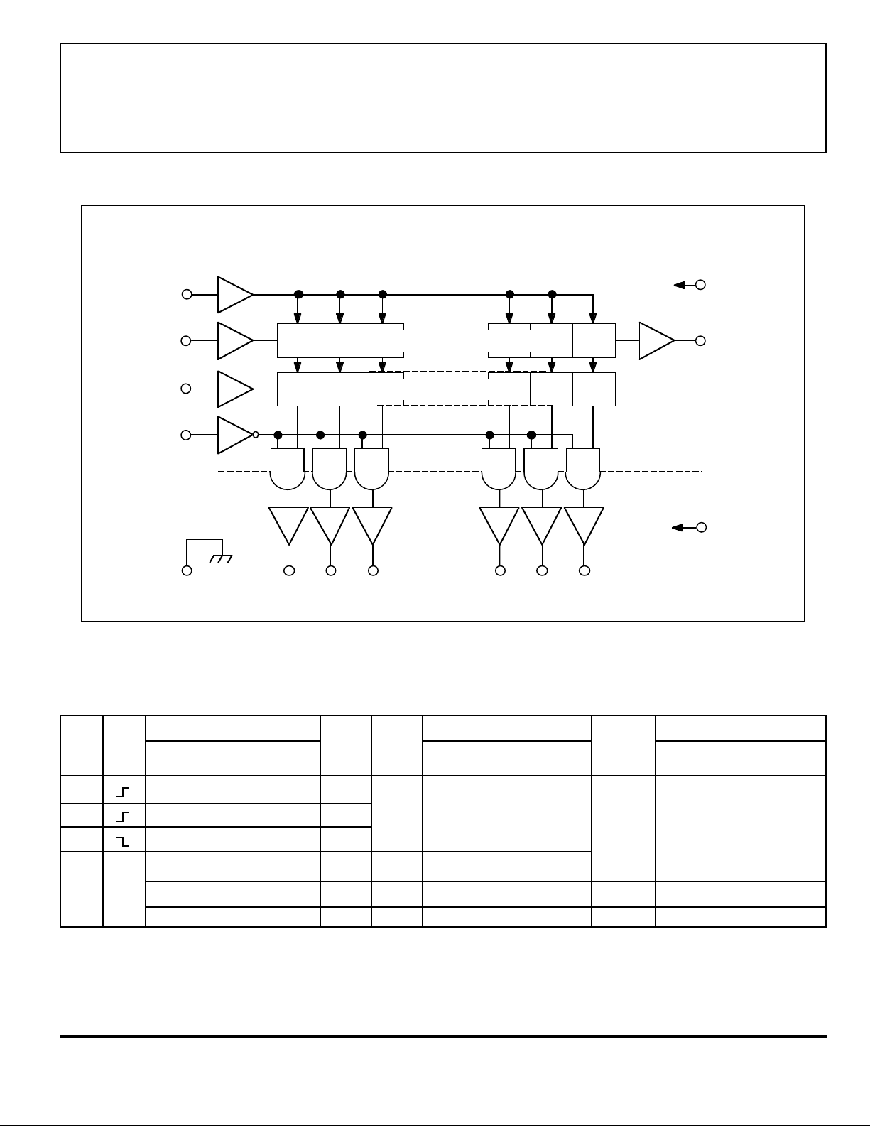
FUNCTIONAL BLOCK DIAGRAM
6810
10-BIT SERIAL-INPUT,
CLOCK
SERIAL
DATA IN
STROBE
BLANKING
GROUND
OUT1OUT
SERIAL-PARALLEL SHIFT REGISTER
LATCHES
OUT
2
3
OUT
N
V
DD
MOS
BIPOLAR
V
BB
LOGIC
SUPPLY
SERIAL
DATA OUT
LOAD
SUPPLY
Dwg. FP-013-1
TRUTH TABLE
Serial Shift Register Contents Serial Latch Contents Output Contents
Data Clock Data Strobe
Input Input I
1I2I3
HHR
LLR
XR
1R2R3
XXX...X X X L R1R2R3... R
P1P2P3... P
L = Low Logic Level H = High Logic Level X = Irrelevant P = Present State R = Previous State
www.allegromicro.com
1R2
1R2
... I
... R
... R
... R
N-1IN
N-2RN-1
N-2RN-1
N-1RN
N-1PN
Output Input I1I2I3... I
R
N-1
R
N-1
R
N
P
N
HP1P2P3... P
X X X ... X X H L L L ... L L
N-1IN
N-1 RN
N-1 PN
Blanklng I1I2I3... I
LP1P2P3... P
N-1
N-1 PN
I
N
 Loading...