


查询6809供应商
A6810xA
OUT
1
OUT
8
2
OUT
7
3
OUT
CLOCK
GROUND
LOGIC
SUPPLY
STROBE
OUT
OUT
6
CLK
4
5
6
V
7
ST
8
5
910
4
LATCHES
REGISTER
REGISTER
LATCHES
DD
ABSOLUTE MAXIMUM RATINGS
at TA = 25°C
Logic Supply Voltage, VDD................... 7.0 V
Driver Supply Voltage, V
Continuous Output Current Range,
I
......................... -40 mA to +15 mA
OUT
Input Voltage Range,
V
....................... -0.3 V to VDD + 0.3 V
IN
Package Power Dissipation,
P
........................................ See Graph
D
Operating Temperature Range, T
(Suffix ‘E–’) .................. -40°C to +85°C
(Suffix ‘S–’) .................. -20
Storage Temperature Range,
T
............................... -55°C to +125°C
S
Caution: These CMOS devices have input
static protection (Class 2) but are still
susceptible to damage if exposed to
extremely high static electrical charges.
................... 60 V
BB
18
17
16
V
15
BB
14
13
BLNK
12
11
A
°C to +85°C
OUT
SERIAL
DATA OUT
LOAD
SUPPLY
SERIAL
DATA IN
BLANKING
OUT
OUT
OUT
Dwg. PP-029
26182.124B
6809
AND
Data Sheet
6810
DABiC-IV, 10-BIT SERIAL-INPUT,
LATCHED SOURCE DRIVERS
The A6809– and A6810– devices combine 10-bit CMOS shift
registers, accompanying data latches and control circuitry with bipolar
sourcing outputs and pnp active pull downs. Designed primarily to
drive vacuum-fluorescent displays, the 60 V and -40 mA output ratings
also allow these devices to be used in many other peripheral power
9
10
1
2
3
driver applications. The A6809– and A6810– feature an increased data
input rate (compared with the older UCN/UCQ5810-F) and a controlled output slew rate. The A6809xLW and A6810xLW are identical
except for pinout.
The CMOS shift register and latches allow direct interfacing with
microprocessor-based systems. With a 3.3 V or 5 V logic supply,
typical serial-data input rates are up to 33 MHz.
A CMOS serial data output permits cascade connections in applications requiring additional drive lines. Similar devices are avail-able as
the A6811– (12 bits), A6812– (20 bits), and A6818– (32 bits).
The A6809– and A6810– output source drivers are npn Darlingtons, capable of sourcing up to 40 mA. The controlled output slew rate
reduces electromagnetic noise, which is an important consideration in
systems that include telecommunications and/or microprocessors and
to meet government emissions regulations. For inter-digit blanking, all
output drivers can be disabled and all sink drivers turned on with a
BLANKING input high. The pnp active pull-downs will sink at least
2.5 mA.
All devices are available in two temperature ranges for optimum
performance in commercial (suffix S-) or industrial (suffix E-) applications. The A6810– is provided in three package styles for through-hole
DIP (suffix -A), surface-mount SOIC (suffix -LW), or minimum-area
surface-mount PLCC (suffix -EP). The A6809– is provided in the
SOIC (suffix -LW) only. Copper lead frames, low logic-power dissipation, and low output-saturation voltages allow all devices to source
25 mA from all outputs continuously over the maximum operating
temperature range.
FEATURES
■ Controlled Output Slew Rate
■ High-Speed Data Storage
■ 60 V Minimum
Output Breakdown
■ High Data Input Rate
■ PNP Active Pull-Downs
Complete part number includes a suffix to identify operating
temperature range (E- or S-) and package type (-A, -EP, or -LW).
Always order by complete part number, e.g., A6810SLW .
■ Low Output-Saturation Voltages
■ Low-Power CMOS Logic
and Latches
■ Improved Replacements
for TL4810–, UCN5810–,
and UCQ5810–

6809
ALLOWABLE PACKAGE POWER DISSIPATION IN WATTS
AND
6810
10-BIT SERIAL-INPUT,
LATCHED SOURCE DRIVERS
TYPICAL OUTPUT DRIVER TYPICAL INPUT CIRCUIT
V
BB
OUT
N
Dwg. EP-021-19
A6809xLW
NC
V
BLNK
BB
20
OUT
19
OUT
NO
18
CONNECTION
SERIAL
17
DATA OUT
16
LOAD SUPPLY
SERIAL
15
DATA IN
14
BLANKING
13
OUT
12
OUT
9
10
1
2
OUT
OUT
OUT
CLOCK
GROUND
CONNECTION
LOGIC SUPPLY
NO
STROBE
OUT
1
8
2
7
3
6
4
5
6
7
8
9
5
CLK
NC
V
ST
LATCHES
REGISTER
REGISTER
LATCHES
DD
CLOCK
NC
GROUND
LOGIC
SUPPLY
STROBE
V
DD
IN
Dwg. EP-010-5
A6810xEP
6
OUT
3
2
1
4
CLK
5
6
7
V
DD
8
ST
LATCHES
REGISTER
REGISTER
LATCHES
10
OUT
19
20
SERIAL
18
DATA OUT
V
BLNK
LOAD
17
BB
SUPPLY
NC
16
SERIAL
15
DATA IN
14
BLANKING
OUT
OUT
OUT
OUT
CLOCK
GROUND
LOGIC SUPPLY
STROBE
OUT
OUT
CONNECTION
NO
10 11
4
A6810xLW
1
8
2
7
3
6
4
CLK
5
6
7
ST
8
5
9
4
10
V
NC
LATCHES
REGISTER
REGISTER
LATCHES
DD
BLNK
OUT
3
Dwg. PP-029-9
9
5
OUT
12
11
10
13
1
OUT
Dwg. PP-059
2.5
20
OUT
9
19
OUT
10
SERIAL
18
DATA OUT
17
V
BB
NC
LOAD SUPPLY
SERIAL
16
DATA IN
15
BLANKING
14
OUT
13
OUT
12
OUT
NO
11
CONNECTION
Dwg. PP-029-2
1
2
3
SUFFIX 'EP', R = 59°C/W
2.0
1.5
1.0
0.5
0
25
θJA
SUFFIX 'A', R = 60°C/W
θJA
SUFFIX 'LW', R = 70°C/W
θJA
50 75 100 125 150
AMBIENT TEMPERATURE IN °C
Dwg. GP-024-1
115 Northeast Cutoff, Box 15036
Worcester, Massachusetts 01615-0036 (508) 853-5000
Copyright © 1998, 2000 Allegro MicroSystems, Inc.
10-BIT SERIAL-INPUT,
LATCHED SOURCE DRIVERS
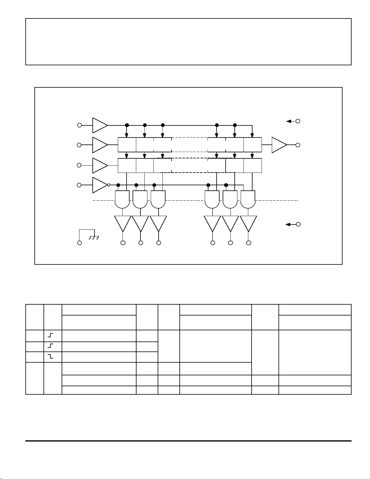
FUNCTIONAL BLOCK DIAGRAM
6809
AND
6810
CLOCK
SERIAL
DATA IN
STROBE
BLANKING
GROUND
OUT1OUT
SERIAL-PARALLEL SHIFT REGISTER
LATCHES
OUT
2
3
OUT
N
V
DD
MOS
BIPOLAR
V
BB
LOGIC
SUPPLY
SERIAL
DATA OUT
LOAD
SUPPLY
Dwg. FP-013-1
TRUTH TABLE
Serial Shift Register Contents Serial Latch Contents Output Contents
Data Clock Data Strobe
Input Input I
HHR
LLR
XR
L = Low Logic Level H = High Logic Level X = Irrelevant P = Present State R = Previous State
www.allegromicro.com
1I2I3
1R2R3
XXX...X X X L R1R2R3... R
P1P2P3... P
1R2
1R2
... I
... R
... R
... R
N-1IN
N-2RN-1
N-2RN-1
N-1RN
N-1PN
Output Input I1I2I3... I
R
N-1
R
N-1
R
N
P
N
HP1P2P3... P
X X X ... X X H L L L ... L L
N-1IN
N-1 RN
N-1 PN
Blanklng I1I2I3... I
LP1P2P3... P
N-1
N-1 PN
I
N
 Loading...